
PolarFire® SoC QSPI 代码编写 测试
1、 首先 将 QSPI 基地址 改为 SC-QSPI 基地址 0x37020100
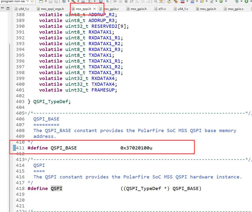
原因如下:
PolarFire FPGA and PolarFire SoC FPGA Programming User Guide
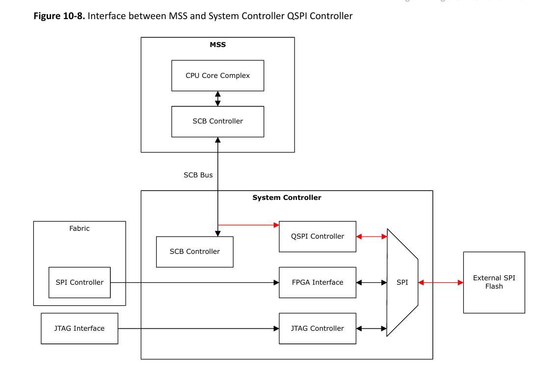
MSS connects to the system controller QSPI using SCB bus. The QSPI controller allows MSS to access system controller SPI flash memory. Use the MSS QSPI driver in Normal mode to access an external SPI flash memory using QSPI base address as 0x37020100 (this address is part of IOSCB data). The following figure shows the interface between MSS and system controller QSPI controller.
2、 QSPI 初始化
mss_qspi_config_t g_qspi_config = {0};
MSS_QSPI_init();
MSS_QSPI_enable();
g_qspi_config.clk_div = MSS_QSPI_CLK_DIV_30; //Tested OK MICRON_FAST_READ command at MSS_QSPI_CLK_DIV_12
g_qspi_config.sample = MSS_QSPI_SAMPLE_POSAGE_SPICLK;
g_qspi_config.spi_mode = MSS_QSPI_MODE3;
g_qspi_config.xip = MSS_QSPI_DISABLE;
g_qspi_config.io_format = MSS_QSPI_NORMAL;
MSS_QSPI_configure(&g_qspi_config);
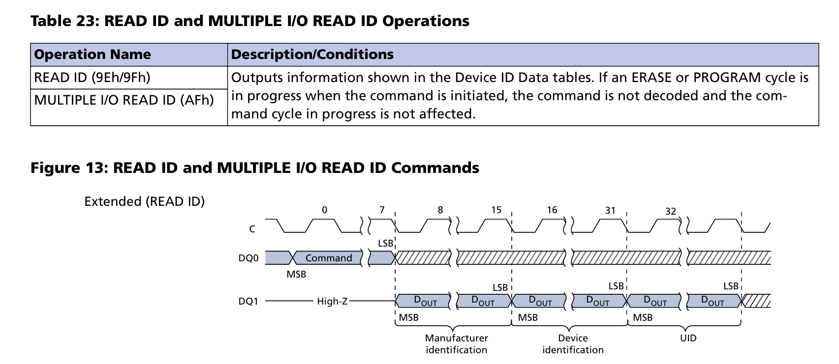
3、使用 命令 0X9F 读取 MT25QL01GBBB8ESF-0SIT ID
// 地址要 4字节对齐
uint8_t tx_buff[1] __attribute__ ((aligned (4))) = {0};
uint8_t rx_buff[3] __attribute__ ((aligned (4))) = {0};
// 读取 DEVICE ID 命令 0x9F
tx_buff[0] = 0x9F;
// 第一个形参 地址的数量 因为 0x9F 读取 ID ,没有地址,这里填写 0
// 第二个形参 发送指令缓冲区指针
// 第三个形参 是要发送的字节数,因为 该函数默认 命令是1个字节,因此 这里 填写 0
// 第四个形参 接收数据缓冲区指针
// 第五个形参 接收数据个数,单位字节
// 最后一个填写 0 ,暂时 未知
MSS_QSPI_polled_transfer_block( 0, tx_buff, 0, rx_buff, 3, 0 );
xprintf( "The flash device manufacturer ID is 0x%02X, memory type ID is 0x%02X, capacity ID is 0x%02X.\n",
rx_buff[0], rx_buff[1], rx_buff[2] );
输出结果:
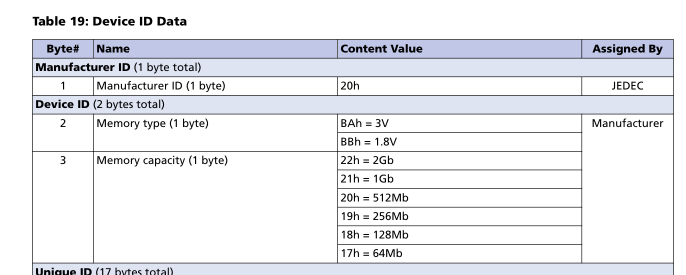
The flash device manufacturer ID is 0x20, memory type ID is 0xBA, capacity ID is 0x21.
移植 SFUD: 一款使用 JEDEC SFDP 标准的串行 (SPI) Flash 通用驱动库 后 :
[SFUD]Find a Micron flash chip. Size is 134217728 bytes.
[SFUD]QSPI_FLASH flash device is initialize success.


 浙公网安备 33010602011771号