
SmartFusion 2 System Services - Programming Service - IAP
IAP 和 ISP 可能会导致两个问题:(Implementing Programming Recovery and In-Application)
1、断电恢复固件后,没有产生复位,导致程序不运行,
请看文档:Appendix 5: Implementing Workaround to Reset the Device after Programming Recovery
2、LSRAM 不能访问
请看文档:Appendix 6: Implementing Workaround to Access Fabric LSRAM after IAP/ISP Program Operation
SmartFusion 2 SOC and IGLOO 2 System Controller (Earlier UG0450)
2.10 Programming Service
The IAP service requests the System Controller to reprogram the device using a bitstream already programmed into flash memory connected to MSS SPI0 or HPMS SPI. When the IAP service is invoked, the System Controller automatically reads the bitstream from the SPI flash memory connected to the MSS SPI0 or HPMS SPI and programs the device. The SPI peripheral must be configured by the user before initiating this request (also accounting for any change in clock frequency due to fabric power down). At the time the request is initiated, the user must guarantee exclusive access of MSS SPI0 or HPMS SPI. The MSS SPI0 or HPMS SPI core is accessed directly through the SII Master. A single read operation (SPI command 0BH) is sent to the SPI flash and bytes are then read through the SII Master and passed along to the programming engine.
- IAP服务请求系统控制器 使用 已编程至MSS SPI0或HPMS SPI连接闪存中的比特流重新配置设备。
- 当调用IAP服务时,系统控制器会自动从MSS SPI0或HPMS SPI连接的SPI闪存读取比特流并对设备进行编程。
- 在发起此请求前,用户必须预先配置SPI外设(同时需考虑由于 fabric 电源关闭可能导致的时钟频率变化)。
- 发起请求时,用户必须确保独占MSS SPI0或HPMS SPI的访问权限。
- MSS SPI0或HPMS SPI内核通过SII主控制器直接访问,系统会向SPI闪存发送单次读取操作(SPI指令0BH),随后通过SII主控制器读取字节数据并传输至编程引擎。
In SmartFusion 2, the Cortex-M3 processor remains active and continues to operate during IAP service execution, but it requires to execute the code from eSRAM if the eNVMs are being reprogrammed.
在SmartFusion 2中,Cortex-M3处理器在执行IAP服务期间保持活动状态并持续运行,但若需重新编程eNVM存储器,则处理器需要从eSRAM执行代码。
If MODE is AUTHENTICATE, the fabric and MSS/HPMS are left operational while the bitstream is authenticated. If MODE is VERIFY, the device is automatically placed in the Flash*Freeze state for the duration of the verify operation and automatically awakened upon completion. The service response is sent after the Flash*Freeze exit stage.
若模式设为AUTHENTICATE,则在认证比特流期间,可编程逻辑单元和MSS/HPMS子系统将保持运行状态;若模式设为VERIFY,设备会在验证操作期间自动进入FlashFreeze冻结状态,并在操作完成后自动唤醒。服务响应将在FlashFreeze退出阶段后发送。
If MODE is PROGRAM, the device is automatically placed in the Flash*Freeze state before programming commences. The MSS and Cortex-M3 processor or HPMS gets reset upon completion of the PROGRAM operation. The service response is sent after the MSS/HPMS reset. If the programming operation is successful, the user design is automatically restarted to initialize the new version of the design. If the programming operation fails, the design is left in the Flash*Freeze configuration and allows to recover from the problem. In this mode, the device components (FPGA fabric, eNVM, and security settings) are programmed based on the payload data available in a bitstream file that is stored in the SPI Flash memory. For example, if the bitstream file contains only FPGA fabric payload data, then this service programs only FPGA fabric portion of the device.
- 若模式设为PROGRAM,设备将在编程操作开始前自动进入Flash*Freeze冻结状态。MSS与Cortex-M3处理器或HPMS子系统会在PROGRAM操作完成后执行复位,服务响应将在MSS/HPMS复位后发送。
- 若编程操作成功,用户设计将自动重启以初始化新版本设计;
- 若编程失败,设计将保持Flash*Freeze配置状态,允许从故障中恢复。在此模式下,设备组件(FPGA可编程逻辑单元、eNVM存储器和安全设置)将根据存储在SPI闪存中的比特流文件有效载荷数据进行编程。
- 例如,若比特流文件仅包含FPGA可编程逻辑单元载荷数据,则本服务仅对设备的FPGA可编程逻辑单元部分进行编程。
IAP 接口:
/*-------------------------------------------------------------------------*//**
The IAP Service requests the System Controller to reprogram the device using
a bitstream already programmed into MSS SPI 0. The IAP Service is initiated by
a call to MSS_SYS_initiate_IAP(). The IAP Service can:
- authenticate a programming bitstream
- program a bitstream
- verify that a programming bitstream has been correctly programmed

@param mode
The mode parameter specifies IAP service to perform. It can be one of:
- MSS_SYS_PROG_AUTHENTICATE
- MSS_SYS_PROG_PROGRAM
- MSS_SYS_PROG_VERIFY

@param bitstream_spi_addr
The bitstream_spi_addr parameter specifies the address of the programming
bitstream within the SPI flash connected to MSS SPI 0.

@return
The MSS_SYS_initiate_IAP function will receive one of the following status
codes:
- MSS_SYS_SUCCESS
- MSS_SYS_CHAINING_MISMATCH
- MSS_SYS_UNEXPECTED_DATA_RECEIVED
- MSS_SYS_INVALID_ENCRYPTION_KEY
- MSS_SYS_INVALID_COMPONENT_HEADER
- MSS_SYS_BACK_LEVEL_NOT_SATISFIED
- MSS_SYS_DSN_BINDING_MISMATCH
- MSS_SYS_ILLEGAL_COMPONENT_SEQUENCE
- MSS_SYS_INSUFFICIENT_DEV_CAPABILITIES
- MSS_SYS_INCORRECT_DEVICE_ID
- MSS_SYS_UNSUPPORTED_BITSTREAM_PROT_VER
- MSS_SYS_VERIFY_NOT_PERMITTED_ON_BITSTR
- MSS_SYS_INVALID_DEVICE_CERTIFICATE
- MSS_SYS_ABORT
- MSS_SYS_NVM_VERIFY_FAILED
- MSS_SYS_DEVICE_SECURITY_PROTECTED
- MSS_SYS_PROGRAMMING_MODE_NOT_ENABLED
- MSS_SYS_ENVM_PROGRAMMING_OPERATION_FAIL
- MSS_SYS_ENVM_VERIFY_OPERATION_FAIL
- MSS_SYS_ACCESS_ERROR
- MSS_SYS_PUF_ACCESS_ERROR
- MSS_SYS_BAD_COMPONENT
- MSS_SYS_SERVICE_DISABLED_BY_USER
*/
uint8_t MSS_SYS_initiate_IAP
(
uint8_t mode,
uint32_t bitstream_spi_addr
);
This demo design explains how to implement the Programming Recovery and In-Application Programming (IAP) features of the SmartFusion2 device. Programming Recovery feature allows the device to automatically recover from a power failure during a programming operation. When Programming Recovery option is enabled, the device is programmed with the Golden Image that is stored in the external flash memory. IAP is a SmartFusion2 device programming feature, which is used to reprogram the device for design iterations and field upgrades. By using the IAP feature, the application reprograms the flash components of the SmartFusion2 device. IAP is a two step process:
1. Used to transfer the image to SPI flash memory.
2. Does the programming of device. There are different ways to transfer the IAP and Golden images from the Host PC to on-board external serial peripheral interface (SPI) flash.
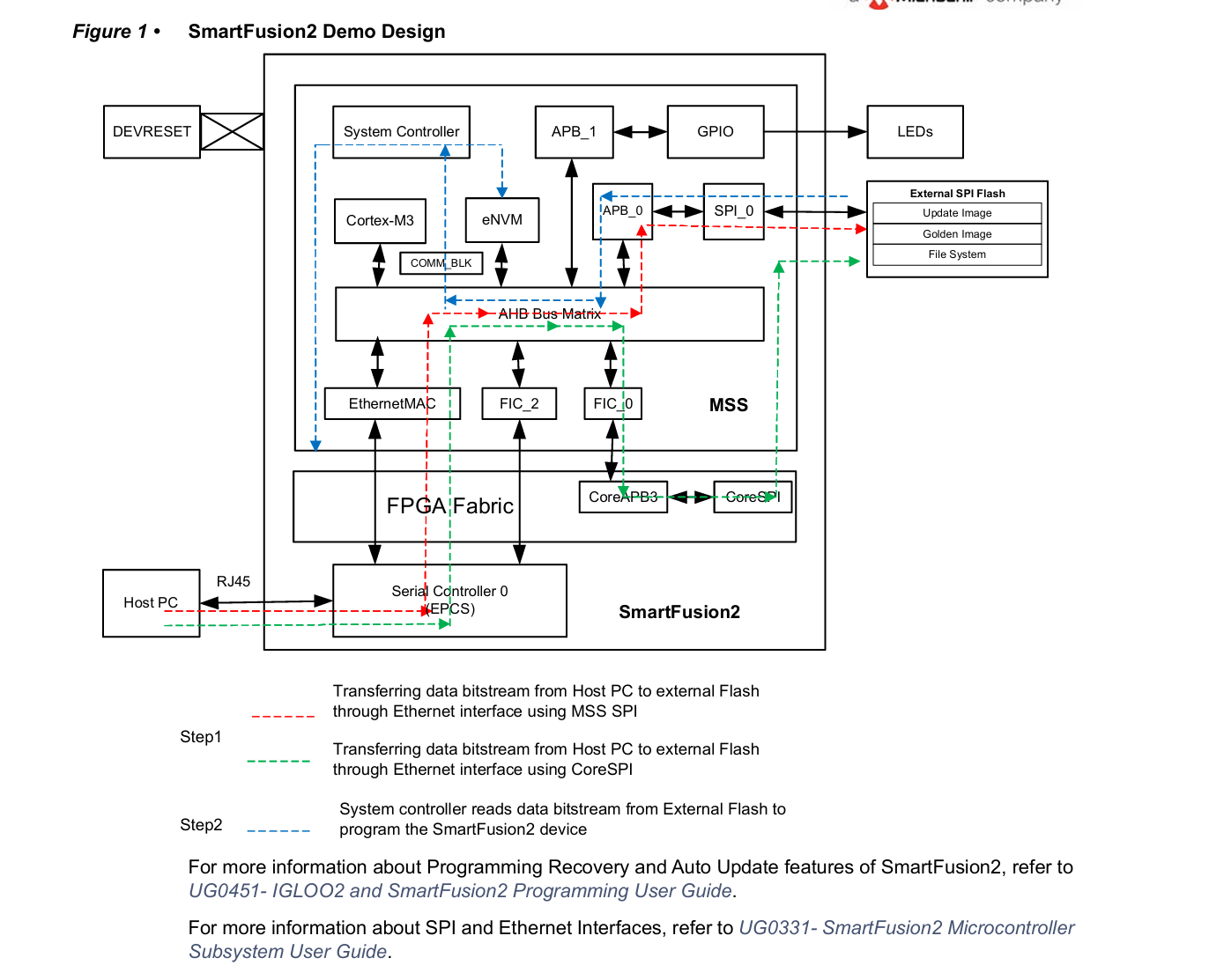
For example, SmartFusion2 supported microcontroller subsystem (MSS) peripherals such as universal asynchronous receiver/transmitter (UART), universal serial bus (USB), peripheral component interconnect express (PCIe), and Ethernet interfaces are used to load the images to the SPI flash memory. In this demo trivial file transfer protocol (TFTP)/Ethernet interface is used for loading SPI flash memory. The following figure shows the data flow of the design. The arrows that are highlighted in red show the data flow between the Host PC and on-board external SPI flash memory using the Ethernet interface. The ARM Cortex-M3 processor copies the programming data from the Host PC to the SPI flash using the Ethernet interface. The arrows that are highlighted in blue show the system controller reading the data from external SPI flash memory to program the SmartFusion2 device. In this demo design, the SPI flash images contain information to program both embedded nonvolatile memory (eNVM) and FPGA fabric.
本演示设计阐述了如何在SmartFusion2器件中实现编程恢复与在线应用编程(IAP)功能。编程恢复功能可使器件在编程操作期间发生电源故障时自动恢复。当启用编程恢复选项时,器件将使用存储在外部闪存中的黄金映像进行编程。
IAP是SmartFusion2器件的编程特性,可用于通过设计迭代和现场升级对器件进行重新编程。通过IAP功能,应用程序可对SmartFusion2器件的闪存组件进行重新编程。IAP操作包含两个步骤:
-
将映像传输至SPI闪存
-
执行器件编程操作
从主机PC向板载外部串行外设接口(SPI)闪存传输IAP及黄金映像存在多种方式。例如,可采用SmartFusion2支持的微控制器子系统(MSS)外设——如通用异步收发器(UART)、通用串行总线(USB)、外围组件快速互连(PCIe)以及以太网接口——将映像加载至SPI闪存。本演示采用简单文件传输协议(TFTP)/以太网接口实现SPI闪存加载。
上图展示了本设计的数据流向。红色高亮箭头表示通过以太网接口在主机PC与板载外部SPI闪存之间的数据传输路径,ARM Cortex-M3处理器通过以太网接口将编程数据从主机PC复制至SPI闪存。蓝色高亮箭头表示系统控制器从外部SPI闪存读取数据并对SmartFusion2器件进行编程的过程。
本演示设计中,SPI闪存映像包含用于编程嵌入式非易失性存储器(eNVM)和FPGA可编程逻辑单元的双重信息。
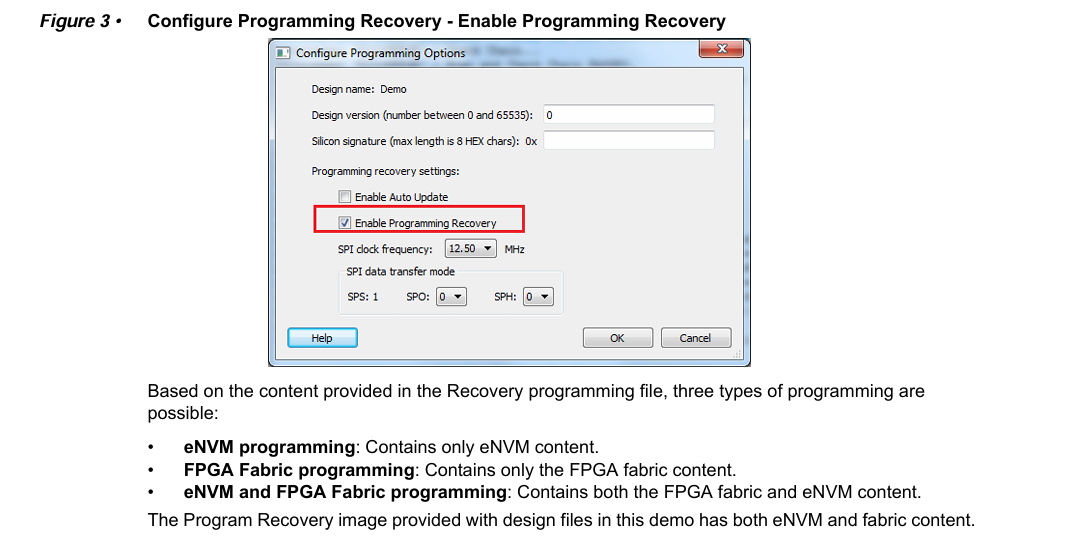
Programming Recovery Programming recovery,
if enabled, automatically recovers from a power failure during a programming operation. The Programming Recovery option is enabled using the Libero SoC software. To enable the Programming Recovery feature, open the Libero Project and select Configure Programming Recovery option in Design Flow window. In the Configure Program Recovery window, select Enable Programming Recovery check box as shown in the following figure.
编程恢复功能
(若启用)可在编程操作期间发生电源故障时实现自动恢复。该功能需通过Libero SoC软件启用:打开Libero项目后,在设计流程窗口中选择"配置编程恢复"选项,在弹出的配置窗口中选择"启用编程恢复"复选框(如下图所示)。
根据恢复编程文件所含内容,支持以下三种编程类型:
• eNVM编程:仅包含eNVM存储器内容
• FPGA可编程逻辑单元编程:仅包含FPGA可编程逻辑单元内容
• eNVM与FPGA可编程逻辑单元联合编程:同时包含可编程逻辑单元和eNVM存储器内容
本演示随设计文件提供的编程恢复映像采用第三种类型,同时包含eNVM存储器和可编程逻辑单元内容。
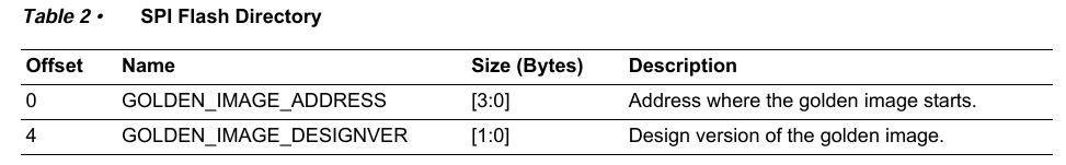
The Programming Recovery option requires an external SPI flash to be connected to MSS SPI_0. External SPI flash needs to be loaded with a SPI directory, Golden Image. The SPI directory provides the address of the Golden image and its design version as listed in the following table.
编程恢复功能要求将外部SPI闪存连接至MSS SPI_0接口。
该外部SPI闪存需加载SPI目录及Golden Image,其中SPI目录需提供Golden Image的存储地址及其设计版本号(如下表所示)。
Create a directory in the SPI flash to provide the address for Golden Image and design version. On the SmartFusion2 Security Evaluation Kit board, the flash memory size is 8 MB. Depending on the size of the programming file, the SPI flash memory is configured in the SoftConsole project as follows: • 0x0 - 0xFFF is for loading SPI Directory • 0x1000 - 0x3FFFFF is for loading Golden Image • 0x400000 - 0x7FFFFF is for loading IAP Image Note: All these addresses are configured in the SoftConsole project and same address needs to be entered while creating the SPI directory. Using TFTP/Ethernet SPI Directory, Golden image, and IAP images are transferred to SPI addresses 0x0, 0x1000, and 0x400000 respectively.
在SPI闪存中创建目录以提供 Golden Image 的存储地址及设计版本号。
基于SmartFusion2安全评估套件板载的8 MB闪存容量,需根据编程文件大小在SoftConsole项目中按以下方式配置SPI闪存:
• 0x0 - 0xFFF:分配予SPI目录加载
• 0x1000 - 0x3FFFFF:分配予黄金映像加载
• 0x400000 - 0x7FFFFF:分配予IAP映像加载
注:上述地址均需在SoftConsole项目中配置,且创建SPI目录时需输入相同地址。通过TFTP/以太网协议,SPI目录、黄金映像和IAP映像将分别传输至SPI闪存的0x0、0x1000及0x400000地址。
libero Creating SPI Directory
The following steps describe how to create an SPI directory:
1. To create SPI directory, open Libero project and select Export Bit Stream from Design Flow window. The Export Bitstream window is displayed as shown in the following figure.
2. Select Export SPI Directory for programming recovery check-box and click Specify SPI Directory.
以下步骤描述如何创建SPI目录:
-
打开Libero项目,在设计流程窗口中选择"Export Bit Stream"(导出比特流)选项,此时将显示如下图所示的导出比特流窗口
-
勾选"Export SPI Directory for programming recovery"(导出用于编程恢复的SPI目录)复选框,并点击"Specify SPI Directory"(指定SPI目录路径)按钮
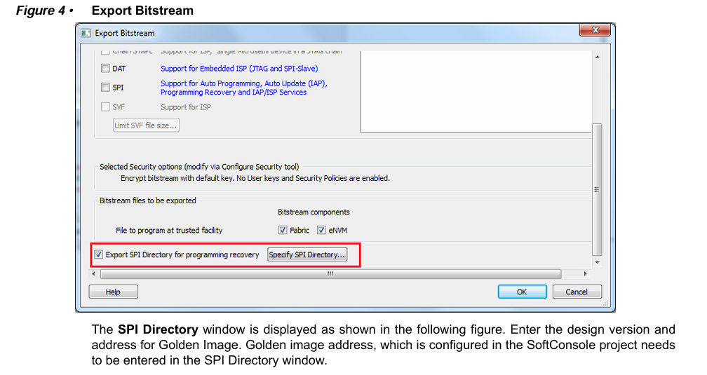
此时将显示如下图所示的SPI目录配置窗口。需在此窗口中输入设计版本号及黄金映像(Golden Image)的存储地址。请注意,此处输入的黄金映像地址必须与SoftConsole项目中配置的地址完全一致。
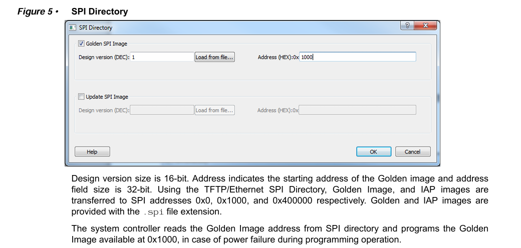
设计版本号为16位宽度,地址字段指示黄金映像的起始地址且为32位宽度。通过TFTP/以太网协议,SPI目录、黄金映像及IAP映像将分别传输至SPI闪存的0x0、0x1000与0x400000地址。
黄金映像与IAP映像均采用.spi文件扩展名。
系统控制器将从SPI目录读取黄金映像地址,若编程操作期间发生断电,将执行存储在0x1000地址的黄金映像编程恢复。
IAP
The IAP feature in SmartFusion2 devices is a two-step process.
Step1: Loading SPI Flash with Programming Image
The Cortex-M3 processor receives the bitstream data from the Host PC through the Ethernet interface and writes to the external SPI flash memory connected to the MSS SPI_0 controller.
Step 2: Initiating the IAP Service
The bitstream data is first verified by requesting the AUTHENTICATE IAP service from the system controller.
SmartFusion2器件的在线应用编程(IAP)功能包含两个执行步骤:
步骤一:向SPI闪存加载编程映像
Cortex-M3处理器通过以太网接口接收来自主机PC的比特流数据,并将其写入连接至MSS SPI_0控制器的外部SPI闪存。
步骤二:启动IAP服务
首先通过向系统控制器请求AUTHENTICATE(认证)IAP服务来验证比特流数据。
The system controller reads the bitstream data from external SPI flash using the SPI interface to check the data integrity of the bitstream data. During authentication, the remainder of the device functions normally. On successful authentication, the Cortex-M3 processor initiates a PROGRAM IAP system controller system service. The system controller fetches the bitstream data from the SPI flash and programs the flash components of the SmartFusion2 device. Programming can be done for the FPGA fabric, eNVM, or both FPGA fabric and eNVM.
系统控制器通过SPI接口从外部SPI闪存读取比特流数据以校验其完整性。
认证过程中,器件其余功能仍保持正常运行。
当认证成功后,Cortex-M3处理器将启动PROGRAM(编程)IAP系统控制器服务。
系统控制器随即从SPI闪存获取比特流数据,并对SmartFusion2器件的闪存组件进行编程。该编程操作可针对FPGA可编程逻辑单元、eNVM存储器,或同时针对两者实施。
The system controller executes the IAP services in the following modes: Authenticate: System controller IAP service validates the integrity of the programming bitstream. For security and reliability reasons, Microsemi recommends that the bitstream must be authenticated before the program is executed, using the Authenticate Operation mode. The SmartFusion2 device application must commit the bitstream for programming, only after successful authentication and the integrity of the bitstream is validated.
系统控制器通过以下模式执行IAP服务:
认证模式(Authenticate):系统控制器IAP服务验证编程比特流的完整性。基于安全性与可靠性考量,Microsemi建议在执行编程操作前必须通过认证操作模式对比特流进行验证。SmartFusion2器件应用程序必须在成功完成认证且比特流完整性验证通过后,方可提交比特流执行编程操作。
Program: Depending on the programming bitstream, system controller IAP service programs the following:
• eNVM programming: The IAP programming service programs only the eNVM. In this case, the input programming file contains has only the eNVM content.
• FPGA fabric programming: The IAP programming service programs only the FPGA fabric. In this case, the input programming file contains has only the FPGA fabric content.
• eNVM and FPGA fabric programming: The IAP programming service programs both the FPGA fabric and eNVM. In this case, the input programming file contains both the FPGA fabric and eNVM content.
编程模式(Program):根据编程比特流内容,系统控制器IAP服务可执行以下编程操作:
• eNVM存储器编程:IAP编程服务仅对eNVM存储器进行编程。此时输入编程文件仅包含eNVM存储器内容。
• FPGA可编程逻辑单元编程:IAP编程服务仅对FPGA可编程逻辑单元进行编程。此时输入编程文件仅包含可编程逻辑单元内容。
• 联合编程:IAP编程服务同时编程FPGA可编程逻辑单元与eNVM存储器。此时输入编程文件同时包含可编程逻辑单元和eNVM存储器内容。
本演示随设计文件提供的IAP映像同时包含eNVM存储器与可编程逻辑单元内容。
Verify: System controller IAP service verifies the content of the SmartFusion2 device against the programming bitstream data that is stored in the SPI flash memory.
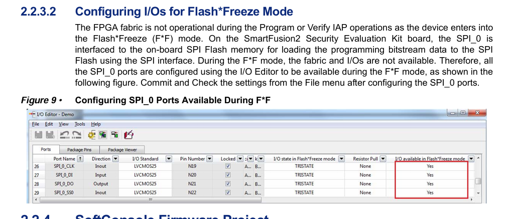
Note: The FPGA fabric is not operational during Program or Verify operations as the device enters into the Flash*Freeze (F*F) mode.
验证模式(Verify):系统控制器IAP服务将SmartFusion2器件的现有内容与存储在SPI闪存中的编程比特流数据进行校验比对。
注:在执行编程或验证操作期间,由于设备会进入FlashFreeze(FF)冻结模式,FPGA可编程逻辑单元将处于非工作状态。
LWIP 和 FreeRTOS 翻译跳过!
2.2.3 Hardware Implementation 硬件实现
In this demo design, the following blocks are configured in the Libero hardware project:
• MSS GPIO block is enabled and configured as: GPIO_0 to GPIO_7 as outputs and connected LEDs.
• M3_CLK clock is configured to 100 MHz.
• MSS SPI_0 controller is enabled to access the external SPI flash memory.
• MMUART1 is enabled for RS-232 communication on the SmartFusion2 Security Evaluation Kit board.
• The MSS TSEMAC is configured for the ten-bit interface (TBI) operation.
• The SERDES_IF_2 in the SmartFusion2 device is configured for EPCS Lane3.
在本演示设计中,Libero硬件项目内已对以下功能模块进行配置:
• 启用MSS GPIO模块并配置为:GPIO_0至GPIO_7设置为输出模式,连接至LED指示灯
• M3_CLK时钟配置为100 MHz
• 启用MSS SPI_0控制器以访问外部SPI闪存 , 注意 这里 PCB设计时, 一定要将 SPI FLASH 接到 特定的引脚上,否则 IAP 无法使用!!!!!!!!!!!!!!!!!!
• 启用MMUART1实现SmartFusion2安全评估套件板上的RS-232通信
• MSS TSEMAC模块配置为十位接口(TBI)工作模式
• SmartFusion2器件中的SERDES_IF_2接口配置为EPCS Lane3通道
2.2.3.1 Standby Clock Source Configuration
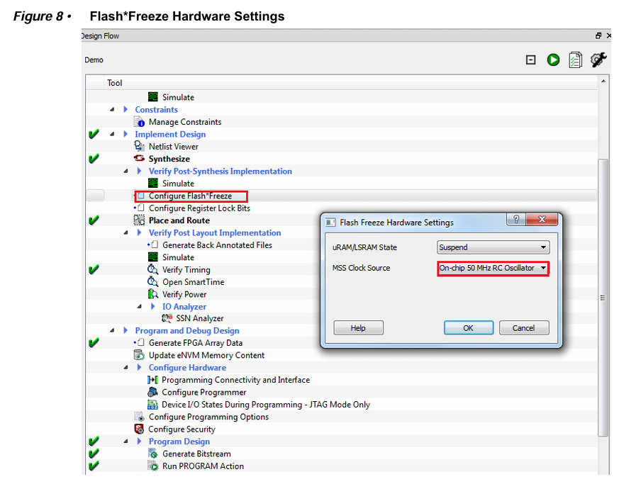
The standby clock source for the MSS in the F*F mode is configured to On-chip 50 MHz RC Oscillator using the Flash*Freeze Hardware Settings dialog box in the Libero SoC software, as shown in the following figure.
A higher MSS clock frequency is required in the F*F mode to meet the SPI communication speed requirements.
2.2.3.1 待机时钟源配置
在Libero SoC软件中,通过如图所示的FlashFreeze硬件设置对话框,已将FF模式下MSS的待机时钟源配置为片内50 MHz RC振荡器。
F*F模式下需要更高的MSS时钟频率以满足SPI通信速率要求。
在执行编程(Program)或验证(Verify)IAP操作期间,由于设备将进入FlashFreeze(FF)冻结模式,FPGA可编程逻辑单元将停止工作。
在SmartFusion2安全评估套件板上,SPI_0接口与板载SPI闪存连接,用于通过SPI接口将编程比特流数据加载至SPI闪存。
在F*F模式期间,可编程逻辑单元与I/O端口均不可用,因此需通过I/O编辑器配置所有SPI_0端口使其在F*F模式下保持可用(如下图所示)。
配置SPI_0端口后,需从File菜单提交并校验相关设置。


 浙公网安备 33010602011771号