
Entity: shk_to_bram
- File: shk_to_bram.v
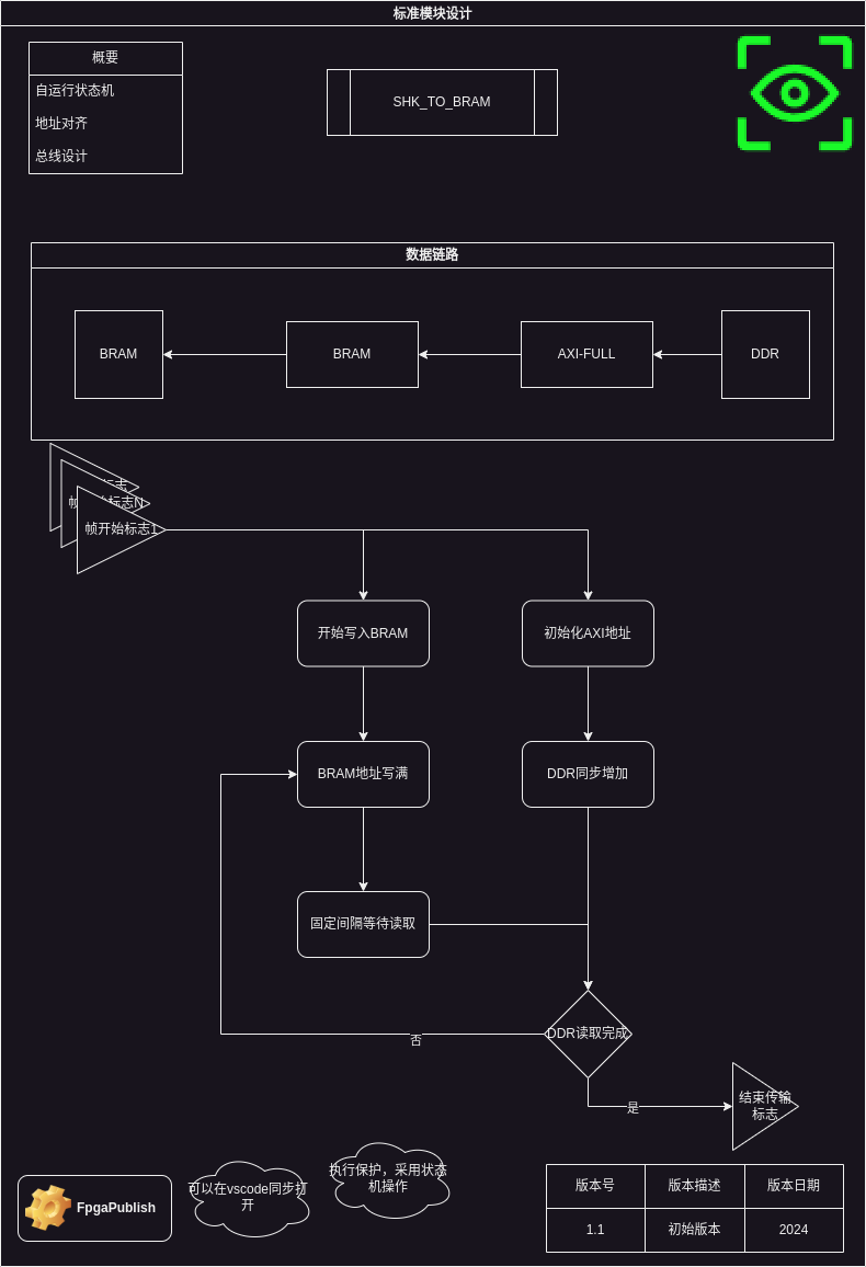
Diagram

Description
Company: FpgaPublish
Engineer: FP
Create Date: 2024/01/12 21:19:05
Revision 0.01 - File Created
Revision 0.02 - add exception info solve

Generics
| Generic name | Type | Value | Description |
|---|---|---|---|
| MD_SIM_ABLE | 0 | mode in sim mode enable | |
| WD_FRAME_START | 3 | width of frame start | |
| NB_START_ADDR0 | 32'h0000_0000 | ddr start addr 0 | |
| NB_START_ADDR1 | 32'h0010_0000 | ddr start addr 1 | |
| NB_START_ADDR2 | 32'h0020_0000 | ddr start addr 2 | |
| NB_START_ADDR3 | 32'h0020_0000 | ddr start addr 2 | |
| NB_START_ADDR4 | 32'h0020_0000 | ddr start addr 2 | |
| NB_START_ADDR5 | 32'h0020_0000 | ddr start addr 2 | |
| NB_START_ADDR6 | 32'h0020_0000 | ddr start addr 2 | |
| NB_START_ADDR7 | 32'h0020_0000 | ddr start addr 2 | |
| NB_FRAME_ALLS | 720 | ddr read all times | |
| WD_SHK0_DATA | 32 | width of shake data | |
| WD_SHK0_ADDR | 32 | width of shake address | |
| NB_SHK0_ONCE | 2048 | ddr read addr once | |
| NB_WR_DELAY | 1000 | write data delay | |
| WD_BRAM_DAT | 32 | width of bram data | |
| WD_BRAM_ADR | 9 | width of bram address | |
| WD_BRAM_WEN | 1 | width of bram write en | |
| WD_ERR_INFO | 4 | width of error info |
Ports
| Port name | Direction | Type | Description |
|---|---|---|---|
| i_sys_clk | input | in system clock | |
| i_sys_resetn | input | in system reset_n | |
| i_frame_start_trig | input | [WD_FRAME_START-1:0] | frame start |
| o_bram_full_trig | output | bram write full | |
| m_err_shk_info1 | output | [WD_ERR_INFO-1:0] | [0]frame start in not IDLE state [1]frame start signal format [2]frame once write more than request |
| bram_master | out | Virtual bus | --bram write |
| shake_master | out | Virtual bus | --read DDR |
Virtual Buses
bram_master
| Port name | Direction | Type | Description |
|---|---|---|---|
| m_bram_wr_addr | output | [WD_BRAM_ADR-1:0] | bram address |
| m_bram_wr_clk | output | bram clock | |
| m_bram_wr_din | output | [WD_BRAM_DAT-1:0] | bram data in |
| m_bram_wr_dout | input | [WD_BRAM_DAT-1:0] | bram data out |
| m_bram_wr_en | output | bram enable | |
| m_bram_wr_rst | output | bram reset high | |
| m_bram_wr_we | output | [WD_BRAM_WEN-1:0] | bram write enable |
shake_master
| Port name | Direction | Type | Description |
|---|---|---|---|
| m_shk0_hp_valid | output | ||
| m_shk0_hp_msync | output | master data synchronize | |
| m_shk0_hp_mdata | output | [WD_SHK0_DATA-1:0] | master data value |
| m_shk0_hp_maddr | output | [WD_SHK0_ADDR-1:0] | master address value |
| m_shk0_hp_ready | input | slaver ready shake | |
| m_shk0_hp_ssync | input | slaver data synchronize | |
| m_shk0_hp_sdata | input | [WD_SHK0_DATA-1:0] | slaver data value |
| m_shk0_hp_saddr | input | [WD_SHK0_ADDR-1:0] | slaver address value |
Signals
| Name | Type | Description |
|---|---|---|
| r_frame_start_chose = 0 | reg [WD_FRAME_START-1:0] | frame start chose |
| w_frame_start_addr = 0 | wire [WD_SHK0_DATA-1:0] | frame start address |
| r_bram_full_trig = 0 | reg | frame bram full trig |
| r_bram_wr_addr = 0 | reg [WD_BRAM_ADR-1:0] | bram address |
| r_bram_wr_clk = 0 | reg | bram clock |
| r_bram_wr_dout_d1 = 0 | reg [WD_BRAM_DAT-1:0] | bram data in temp one clock |
| r_bram_wr_din = 0 | reg [WD_BRAM_DAT-1:0] | bram data out |
| r_bram_wr_en = 0 | reg | bram enable |
| r_bram_wr_rst = 0 | reg | bram reset high |
| r_bram_wr_we = 0 | reg [WD_BRAM_WEN-1:0] | bram write enable |
| r_shk0_hp_valid = 0 | reg | master valid shake |
| r_shk0_hp_msync = 0 | reg | master data synchronize |
| r_shk0_hp_mdata = 0 | reg [WD_SHK0_DATA-1:0] | master data value |
| r_shk0_hp_maddr = 0 | reg [WD_SHK0_ADDR-1:0] | master address value |
| r_wr_delay_cnt = 0 | reg [WD_WR_DELAY-1:0] | delay count |
| cstate = IDLE | reg [3:0] | current state |
| r_err_shk_info1 = 0 | reg [WD_ERR_INFO-1:0] | error info |
Constants
| Name | Type | Value | Description |
|---|---|---|---|
| WD_WR_DELAY | (NB_WR_DELAY) | width of NB_WR_DELAY | |
| WD_SHK0_BYTE | WD_SHK0_DATA / 8 | shake data bytes | |
| NB_BRAM_ONC | NB_SHK0_ONCE / WD_SHK0_BYTE | numb of bram once write | |
| IDLE | 0 | state idle | |
| START | 1 | start read ddr | |
| SHK_REQ | 6 | update addr of DDR | |
| SHK_WR | 2 | shake write data to bram | |
| DELAY | 3 | delay wait | |
| SWITCH | 4 | chose if continue | |
| OVER | 5 | object over |
Functions
- LOG2 (input integer N) return (integer)
- calculate LOG2 convert INT by abandon fractional part
Processes
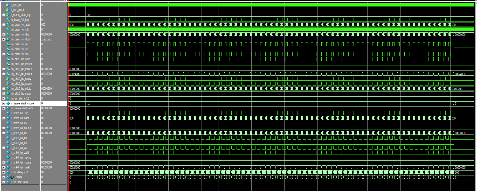
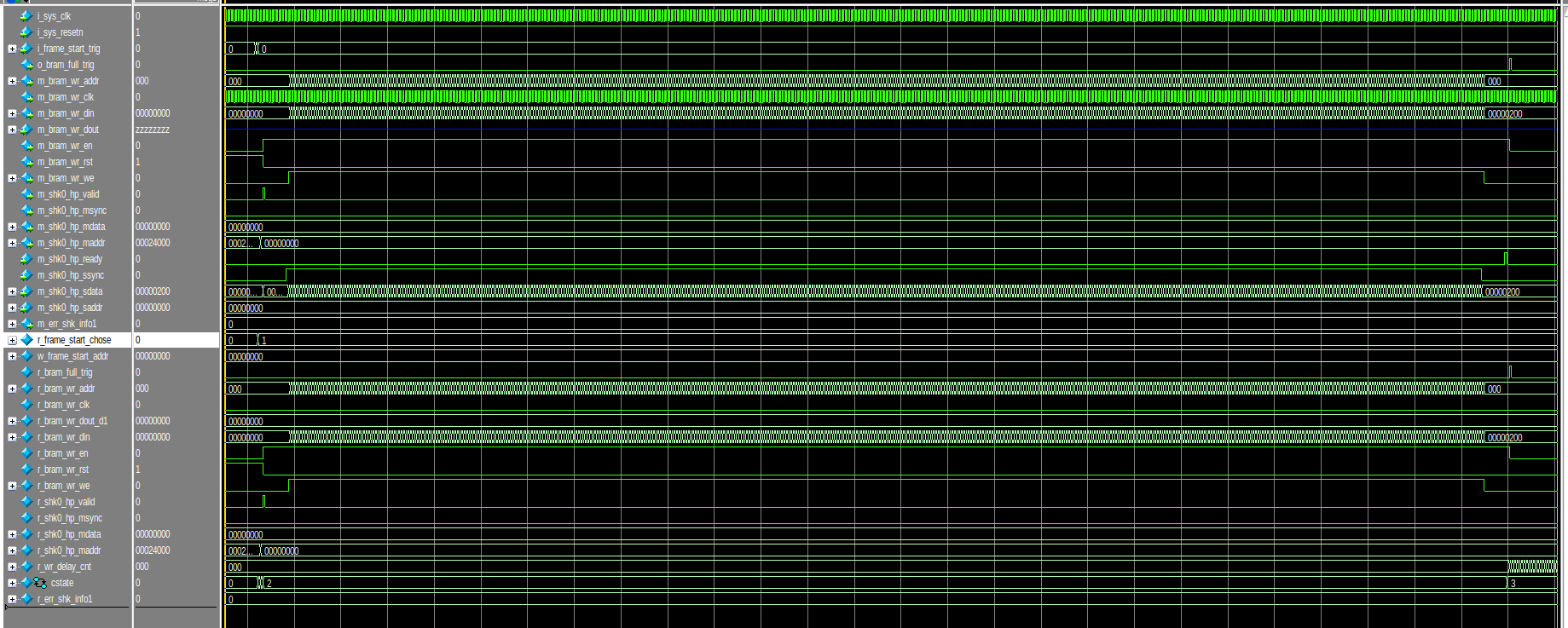
- unnamed: ( @(posedge i_sys_clk) )
- Type: always
- Description
frame info
- unnamed: ( @(posedge i_sys_clk) )
- Type: always
- Description
bram interface
- unnamed: ( @(posedge i_sys_clk) )
- Type: always
- Description
shk hp interface
- unnamed: ( @(posedge i_sys_clk) )
- Type: always
- Description
delay count
State machines
- current state

/*
code
*/
// *******************************************************************************
//!Company: FpgaPublish
//!
//!Engineer: FP
//!
//!Create Date: 2024/01/12 21:19:05
//!
// Design Name:
// Module Name: shk_to_bram
// Project Name:
// Target Devices: ZYNQ7010 | XCZU2CG | Kintex7
// Tool Versions: 2021.1 || 2022.2
// Description:
//         *
// Dependencies:
//         *
// Revision: 0.01
//!----------------------------
//!Revision 0.01 - File Created
//!
//!Revision 0.02 - add exception info solve
//!

// Additional Comments:
//
// *******************************************************************************
`timescale 1ns / 1ps
//! { signal: [
//!  { name: "clk",   wave: "P..............." },
//!  { name: "bus",   wave: "x.==.=.....x.=x.", data: ["start", "wait", "valid", "over"] },
//!  { name: "valid", wave: "0.10............" },
//!  { name: "mdata", wave: "0....3.....0....",data:["data_wr"] },
//!  { name: "maddr", wave: "0.4..0..........",data:["addr-req"] },
//!  { name: "msync", wave: "0....1.....0...." },
//!  { name: "ready", wave: "0............10." },
//!  { name: "sdata", wave: "0...3......0....",data:["data_rd"] },
//!  { name: "saddr", wave: "0...........4.0.",data:["addr-bck"] },
//!  { name: "ssync", wave: "0...1......0...." },
//! ],
//!  head:{
//!     text:'user shk interface',
//!     tick:0,
//!     every:2
//!   }}

module shk_to_bram #(
    //sim mode
    parameter MD_SIM_ABLE = 0,//!mode in sim mode enable
    //frame start
    parameter WD_FRAME_START = 3, //!width of frame start
    parameter NB_START_ADDR0 = 32'h0000_0000, //! ddr start addr 0
    parameter NB_START_ADDR1 = 32'h0010_0000, //! ddr start addr 1
    parameter NB_START_ADDR2 = 32'h0020_0000, //! ddr start addr 2
    parameter NB_START_ADDR3 = 32'h0020_0000, //! ddr start addr 2
    parameter NB_START_ADDR4 = 32'h0020_0000, //! ddr start addr 2
    parameter NB_START_ADDR5 = 32'h0020_0000, //! ddr start addr 2
    parameter NB_START_ADDR6 = 32'h0020_0000, //! ddr start addr 2
    parameter NB_START_ADDR7 = 32'h0020_0000, //! ddr start addr 2

    parameter NB_FRAME_ALLS  = 720 ,          //! ddr read all times
    //shake bus
    parameter WD_SHK0_DATA   = 32,   //! width of shake data
    parameter WD_SHK0_ADDR   = 32,   //! width of shake address
    parameter NB_SHK0_ONCE   = 2048, //! ddr read addr once

    //time delay
    parameter NB_WR_DELAY  = 1000, //! write data delay
    //bram bus
    parameter WD_BRAM_DAT = 32, //! width of bram data
    parameter WD_BRAM_ADR = 9 , //! width of bram address
    parameter WD_BRAM_WEN = 1 , //! width of bram write en
    //error info
    parameter WD_ERR_INFO = 4 //!width of error info
   )(
    //system signals
    input           i_sys_clk   , //!in system clock
    input           i_sys_resetn, //!in system reset_n
    //frame start
    input    [WD_FRAME_START-1:0]   i_frame_start_trig, //!frame start
    output                          o_bram_full_trig  , //!bram write full
    //! @virtualbus bram_master @dir out --bram write
    output   [WD_BRAM_ADR-1:0]  m_bram_wr_addr, //! bram address
    output                      m_bram_wr_clk , //! bram clock
    output   [WD_BRAM_DAT-1:0]  m_bram_wr_din , //! bram data in
    input    [WD_BRAM_DAT-1:0]  m_bram_wr_dout, //! bram data out
    output                      m_bram_wr_en  , //! bram enable
    output                      m_bram_wr_rst , //! bram reset high
    output   [WD_BRAM_WEN-1:0]  m_bram_wr_we  , //! bram write enable
    //! @end
    //! @virtualbus shake_master @dir out --read DDR
    output                      m_shk0_hp_valid,//! master valid shake
    output                      m_shk0_hp_msync,//! master data synchronize
    output   [WD_SHK0_DATA-1:0] m_shk0_hp_mdata,//! master data value
    output   [WD_SHK0_ADDR-1:0] m_shk0_hp_maddr,//! master address value
    input                       m_shk0_hp_ready,//! slaver ready shake
    input                       m_shk0_hp_ssync,//! slaver data synchronize
    input    [WD_SHK0_DATA-1:0] m_shk0_hp_sdata,//! slaver data value
    input    [WD_SHK0_ADDR-1:0] m_shk0_hp_saddr,//! slaver address value
    //! @end

    //![0]frame start in not IDLE state
    //![1]frame start signal format
    //![2]frame once write more than request
    output   [WD_ERR_INFO-1:0]  m_err_shk_info1
);
//========================================================
//function to math and logic
//!calculate LOG2 convert INT by abandon fractional part
function automatic integer LOG2(input integer N);
begin
    N = N - 1;
    for(LOG2 = 0; N > 0; LOG2 = LOG2 + 1)
    begin
        N = N >> 1;
    end
end
endfunction
//========================================================
//localparam to converation and calculate
localparam WD_WR_DELAY  = LOG2(NB_WR_DELAY); //!width of NB_WR_DELAY
localparam WD_SHK0_BYTE = WD_SHK0_DATA / 8; //!shake data bytes
localparam NB_BRAM_ONC  = NB_SHK0_ONCE / WD_SHK0_BYTE;//! numb of bram once write

//========================================================
//register and wire to time sequence and combine
// ----------------------------------------------------------
//! frame info
reg [WD_FRAME_START-1:0]    r_frame_start_chose = 0; //!frame start chose
wire [WD_SHK0_DATA-1:0]     w_frame_start_addr  = 0; //!frame start address
reg                         r_bram_full_trig    = 0; //!frame bram full trig
assign o_bram_full_trig  =  r_bram_full_trig;

// ----------------------------------------------------------
//! bram interface
reg [WD_BRAM_ADR-1:0]  r_bram_wr_addr    = 0; //! bram address
reg                    r_bram_wr_clk     = 0; //! bram clock
reg [WD_BRAM_DAT-1:0]  r_bram_wr_dout_d1 = 0; //! bram data in temp one clock
reg [WD_BRAM_DAT-1:0]  r_bram_wr_din     = 0; //! bram data out
reg                    r_bram_wr_en      = 0; //! bram enable
reg                    r_bram_wr_rst     = 0; //! bram reset high
reg [WD_BRAM_WEN-1:0]  r_bram_wr_we      = 0; //! bram write enable
//connect out
assign m_bram_wr_addr   = r_bram_wr_addr   ;
assign m_bram_wr_clk    = i_sys_clk        ;
assign m_bram_wr_din    = r_bram_wr_din    ;
assign m_bram_wr_en     = r_bram_wr_en     ;
assign m_bram_wr_rst    = r_bram_wr_rst    ;
assign m_bram_wr_we     = r_bram_wr_we     ;
// ----------------------------------------------------------
//! shk interface
reg                      r_shk0_hp_valid = 0; //! master valid shake
reg                      r_shk0_hp_msync = 0; //! master data synchronize
reg [WD_SHK0_DATA-1:0]   r_shk0_hp_mdata = 0; //! master data value
reg [WD_SHK0_ADDR-1:0]   r_shk0_hp_maddr = 0; //! master address value
assign m_shk0_hp_valid = r_shk0_hp_valid;
assign m_shk0_hp_msync = r_shk0_hp_msync;
assign m_shk0_hp_mdata = r_shk0_hp_mdata;
assign m_shk0_hp_maddr = r_shk0_hp_maddr;

// ----------------------------------------------------------
//! delay count
reg [WD_WR_DELAY-1:0] r_wr_delay_cnt = 0;

//========================================================
//always and assign to drive logic and connect
/* end verilog
*/
/* @begin state machine */
//state name
localparam IDLE         = 0; //! state idle
localparam START        = 1; //! start read ddr
localparam SHK_REQ      = 6; //! update addr of DDR
localparam SHK_WR       = 2; //! shake write data to bram
localparam DELAY        = 3; //! delay wait
localparam SWITCH       = 4; //! chose if continue
localparam OVER         = 5; //! object over
//state variable
reg [3:0] cstate = IDLE;//! current state

//state logic
always @(posedge i_sys_clk)
    if(!i_sys_resetn)
    begin
       cstate <= IDLE;
    end
    else if(i_frame_start_trig) //force skip SHK false
    begin
        cstate <= START; //
    end
    else
    begin
        case(cstate)
            IDLE : if(i_frame_start_trig) //whether goto next state
                begin
                    if(1) //which state to go
                    begin
                        cstate <= START;
                    end
                end
            START: if(1) //state change:
                begin
                    if(r_frame_start_chose == 0) //state switch: error frame start
                    begin
                        cstate <= OVER;
                    end
                    else if(1) //state switch: normal start write
                    begin
                        cstate <= SHK_REQ;
                    end
                end
            SHK_REQ: if(1) //state change:
                begin
                    if(1) //state switch:
                    begin
                        cstate <= SHK_WR;
                    end
                end
            SHK_WR: if(m_shk0_hp_ready) //state change: ddr once read over
                begin
                    if(1) //state switch:
                    begin
                        cstate <= DELAY;
                    end
                end
            DELAY: if(r_wr_delay_cnt == NB_WR_DELAY - 1'b1) //state change:
                begin
                    if(1) //state switch:
                    begin
                        cstate <= SWITCH;
                    end
                end
            SWITCH: if(1) //state change:
                begin
                    if(r_shk0_hp_maddr == w_frame_start_addr
                    + NB_SHK0_ONCE * (NB_FRAME_ALLS - 1)) //state switch: address of ddr is full
                    begin
                        cstate <= OVER;
                    end
                    else
                    begin
                        cstate <= SHK_REQ;
                    end
                end
            OVER: if(1) //state change:
                begin
                    if(1) //state switch:
                    begin
                        cstate <= IDLE;
                    end
                end
            default: cstate <= IDLE;
        endcase
    end
/* @end state machine  */
// ----------------------------------------------------------
//! frame info
always@(posedge i_sys_clk)
begin
    if(cstate == IDLE) //state IDLE reset
    begin
        if(i_frame_start_trig)
        begin
            case(i_frame_start_trig)
                'b0000_0001: r_frame_start_chose <= 1;
                'b0000_0010: r_frame_start_chose <= 2;
                'b0000_0100: r_frame_start_chose <= 3;
                'b0000_1000: r_frame_start_chose <= 4;
                'b0001_0000: r_frame_start_chose <= 5;
                'b0010_0000: r_frame_start_chose <= 6;
                'b0100_0000: r_frame_start_chose <= 7;
                'b1000_0000: r_frame_start_chose <= 8;
                default: r_frame_start_chose <= 0; //error
            endcase

        end
        else
        begin
            r_frame_start_chose <= 1'b0;
        end
    end
end
assign w_frame_start_addr = r_frame_start_chose == 1 ? NB_START_ADDR0 :
                            r_frame_start_chose == 2 ? NB_START_ADDR1 :
                            r_frame_start_chose == 3 ? NB_START_ADDR2 :
                            r_frame_start_chose == 4 ? NB_START_ADDR3 :
                            r_frame_start_chose == 5 ? NB_START_ADDR4 :
                            r_frame_start_chose == 6 ? NB_START_ADDR5 :
                            r_frame_start_chose == 7 ? NB_START_ADDR6 :
                            r_frame_start_chose == 8 ? NB_START_ADDR7 :
                            1'b0;
always@(posedge i_sys_clk)
begin
    if(cstate == IDLE) //state IDLE reset
    begin
        r_bram_full_trig <= 1'b0;
    end
    else if(cstate == DELAY)
    begin
        if(r_wr_delay_cnt == 0)
        begin
            r_bram_full_trig <= 1'b1;
        end
        else
        begin
            r_bram_full_trig <= 1'b0;
        end
    end
end
// ----------------------------------------------------------
//! bram interface
always@(posedge i_sys_clk)
begin
    if(cstate == IDLE || cstate == SHK_REQ) //state IDLE reset
    begin
        r_bram_wr_addr <= 1'b0;
    end
    else if(cstate == SHK_WR)
    begin
        if(r_bram_wr_we) //ddr addr count sync with we
        begin
            r_bram_wr_addr <= r_bram_wr_addr + 1'b1;
        end
    end
end
always@(posedge i_sys_clk)
begin
    if(cstate == IDLE) //state IDLE reset
    begin
        r_bram_wr_din <= 1'b0;
    end
    else if(cstate == SHK_WR)
    begin
        r_bram_wr_din <= m_shk0_hp_sdata;//data stream connect
    end
end
always@(posedge i_sys_clk)
begin
    if(cstate == IDLE || cstate == DELAY) //state IDLE reset
    begin
        r_bram_wr_en <= 1'b0;
    end
    else if(cstate == SHK_REQ)
    begin
        r_bram_wr_en <= 1'b1;
    end
end
always@(posedge i_sys_clk)
begin
    if(cstate == IDLE) //state IDLE reset
    begin
        r_bram_wr_rst <= 1'b1;
    end
    else if(cstate == SHK_REQ)
    begin
        r_bram_wr_rst <= 1'b0;
    end
end
always@(posedge i_sys_clk)
begin
    if(cstate == IDLE) //state IDLE reset
    begin
        r_bram_wr_we <= 1'b0;
    end
    else if(cstate == SHK_WR)
    begin
        r_bram_wr_we <= m_shk0_hp_ssync;
    end
end
// ----------------------------------------------------------
//! shk hp interface
always@(posedge i_sys_clk)
begin
    if(cstate == IDLE || cstate == SHK_WR) //state IDLE reset
    begin
        r_shk0_hp_valid <= 1'b0;
    end
    else if(cstate == SHK_REQ)
    begin
        r_shk0_hp_valid <= 1'b1;
    end
end
always@(posedge i_sys_clk)
begin
    if(cstate == START) //state IDLE reset
    begin
        r_shk0_hp_maddr <= w_frame_start_addr;
    end
    else if(cstate == SWITCH)
    begin
        r_shk0_hp_maddr <= r_shk0_hp_maddr + NB_SHK0_ONCE;
    end
end
// ----------------------------------------------------------
//! delay count
always@(posedge i_sys_clk)
begin
    if(cstate == IDLE || cstate == SHK_REQ) //state IDLE reset
    begin
        r_wr_delay_cnt <= 1'b0;
    end
    else if(cstate == DELAY)
    begin
        r_wr_delay_cnt <= r_wr_delay_cnt + 1'b1;
    end
end
//========================================================
//module and task to build part of system

//========================================================
//expand and plug-in part with version
// ----------------------------------------------------------
//! error info

reg [WD_ERR_INFO-1:0] r_err_shk_info1 = 0; //! error info

assign m_err_shk_info1 = r_err_shk_info1;
always@(posedge i_sys_clk)
begin
    if(!i_sys_resetn) //system reset
    begin
        r_err_shk_info1 <= 1'b0; //
    end
    else if(1) //
    begin
        r_err_shk_info1[0] <= i_frame_start_trig && cstate != IDLE;        //frame start not in IDLE state
        r_err_shk_info1[1] <= cstate == START && r_frame_start_chose == 0; //frame start signal format error
        r_err_shk_info1[2] <= cstate == SHK_WR && r_bram_wr_addr > NB_BRAM_ONC; //frame once write more than request
    end
end

//========================================================
//ila and vio to debug and monitor

endmodule

/* end verilog
logic
sim
*/
======== ======\\ ======= -
|| || \\ // \\ /-\
|| || || // // \\
|| || // || // \\
====== ======= || === ========
|| || || \\ // \\
|| || \\ || // \\
|| || \\ // // \\
|| || ======= // \\
作者:绿叶落秋风,专注FPGA技术分析和分享,转载请注明原文链接:https://www.cnblogs.com/electricdream/p/17963241,文中资源链接如下:
1. GITHUB开源仓库
 浙公网安备 33010602011771号