功率开关管的转换效率:IRFP系列MOSFET@Vishay +SiC碳化硅MOSFET@Infinion+ROHM +GaS氮化镓MOSFET@Microchip+Infinion+Wolfspeed+GanSystem
Vishay Intertechnology
[PDF]High-Voltage Silicon MOSFETs, GaN, and SiC: All have a place
WebPhilip Zuk, Director of Market Development, High-Voltage MOSFET Group, Vishay
GaN vs. SiC: Everything You Need To Know, March 30, 2020 Editorial Staff
IGBT: 97.4% 桥式并联双IGBT(STGW60H65DGB),5KW总热功133W风扇必要.
MOSFET: >97.4% 桥式并联双MOSFET(IRFP460),最好有风扇.
IRFP460, Vds=500V, Id=20A(20°,Vgs=10V, Rgs=0.7Ω, 热功率Phot=I²R=280W),
散热好的桥式双管可承8000W有余。淘宝店价格10元/支上下。
SiC碳化硅MOSFET > 99.00%(超低内阻Rds=0.007Ω, 为常规MOSFET的1/100)
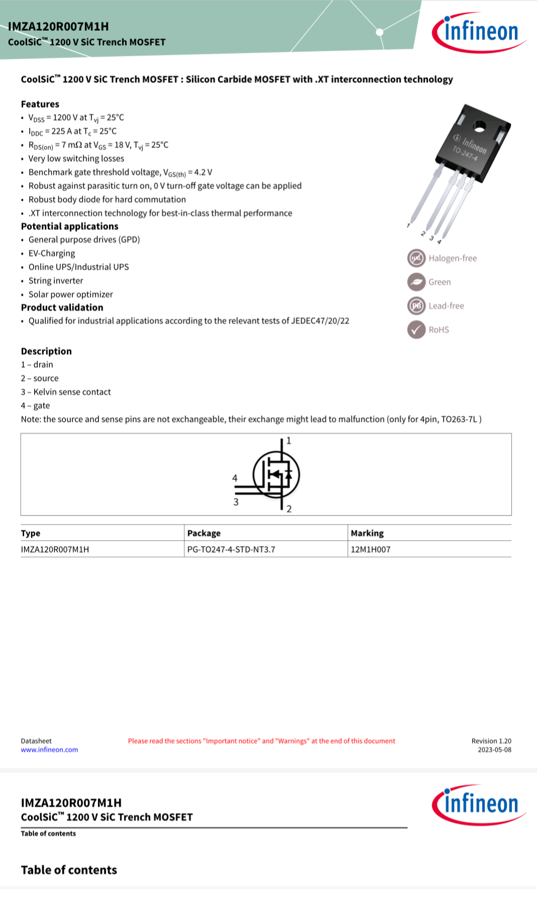
Infinion的CoolSiC硅化碳系列:
IMZA120R007M1H,90美元/支, Vds=1200V, Rds=0.007Ω, 热功率Phot=I²R=280W, Id-max@25°C=225A
即100A的Id时热功率只有70W, 而其正常工作范围:Vds∈[0V,1200V], Id∈[0A,500A]
Advantages
In particular, SiC devices withstand higher voltages, up to 1200V and more,
while GaN devices can withstand lower voltages and power densities;
on the other hand, thanks to the almost zero switch-off times of the GaN devices (high electron mobility with consequent dV/dt greater than 100V/s compared to the 50V/s of the MOSFET Si), these can be used in very high-frequency applications, with unprecedented efficiency and performance. This ideally positive characteristic could prove to be inconvenient: if the parasitic capacitances of the component are not close to zero, current spikes of the order of tens of amperes can be generated, which could cause problems in the electromagnetic compatibility test phase.
SiCs have further advantages on the packages used, due to the possibility of adopting TO-247 and TO-220 which allows the rapid replacement of IGBTs and MOSFETs with the new SiCs, while the GaNs give better results with SMD packages (that are lighter and small but relegated to new projects).
Common design challenges
On the other hand, a common challenge for the two types of devices is related to the design and the construction of gate drivers capable of making the best use of the components-specific characteristics, paying attention to the parasitic components (which must be minimized in order to avoid a weaker performance) and to the levels of applicable voltage (hopefully similar to those used to drive classic silicon components).
Cost differences
In terms of costs, SiC devices are now cheaper and more popular, also because they were made before GaN. However, as it is easy to confirm, costs are only in part related to the production process, and to the market demands, that is why prices will be likely to flatten in the market.
Due to the higher production costs of the GaN substrate, devices that use a GaN “channel” have a Si substrate. In recent months, the Swedish University of Linköping, in collaboration with its spin-off SweGaN, has conducted some research following the idea of using a SiC substrate and a new wafer growth process (called transmorphic heteroepitaxy, which prevents the presence of structural defects), thus obtaining maximum voltages comparable to SiC devices, but capable of working at the frequency of GaN on Si. This research also highlighted how the adoption of this mechanism is able to provide improvements in heat management, a vertical breakdown voltage over 3kV, and a resistance in the ON state less than an order of magnitude compared to today's solutions.
Applications and market share
WBG devices fields of application are still a niche, and R&D still have to better understand how to make the most out of their potential. The largest new technology market is the diode market, but WBG is expected to flood the transistor market over the next 5 years.
Possible applications have started to be hypothesized, and the projections show that electric mobility, telecommunications, and the consumer market are the most plausible.
According to sales forecasts, the most profitable market will be the one involving electric mobility and self-driving vehicles, where the WBG will be used in inverters, onboard charging devices (OBC) and anti-collision systems (LiDAR) and this is obvious, given the thermal characteristics and efficiency of the new devices that matches with the request to optimize the performance of the accumulators.
As for telecommunications, the role of 5G will be the driving force for the WBG, whose millions of stations to be installed will need higher energy efficiency, and will also be smaller and lighter, with a significant gain in performance and cuts on costs.
The consumer market will also involve the massive use of new devices. Wireless power and recharging devices will be mainly affected, thanks to the ever-increasing spread of mobile devices and therefore to the needs of fast-charging.
SiC and GaN devices
Infineon has developed a wide range of SiC and GaN MOSFET devices with their drivers, the CoolSiC and CoolGaN series. Noteworthy is the FF6MR12W2M1_B11 half-bridge module, which is capable of delivering up to 200A at 1200V, with an RDS(on) resistance of only 6mΩ. The module is equipped with two SiC MOSFETs and a NTC temperature sensor, and is suitable for UPS and motor control applications, with an eye to efficiency and thermal dissipation (figure 1).
There is a similar solution in the Microsemi catalog (now Microchip Technology), with the Phase Leg SiC MOSFET module, which makes use of the SP6LI devices family, and allows voltages up to 1700V and currents greater than 200A; the AlN substrate ensures better thermal management, and two SiC Schottky diodes allow for an increase in switching frequencies.
Wolfspeed is keeping up with the market with its CAB450M12XM3, half-bridge device capable of managing voltages up to 1200V and currents of 450A, suitable for working up to 175°C in continuous mode thanks to the use of their third generation MOSFETs with SiN substrate.
When taking a look at the GaN world, it is immediately clear that a variety of devices available is limited. GanSystem offers the GS-065-150-1-D in its catalog, a transistor that makes use of the patented Island Technology, capable of managing up to 650V and 150A at a switching frequency greater than 10MHz.
Finally, with its TP90H050WS FET, which will see the light in mid-2020, Transphorm is working on a GaN device using the TO-247 package whose working voltage can reach 900V, with rising and falling times of about 10nS (Figure 2).
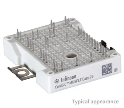
Figure 1: FF6MR12W2M1_B11 half-bridge module
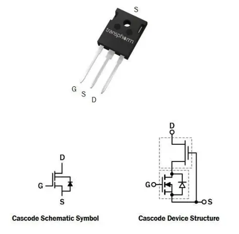
Figure 2: TP90H050WS FET
By Davide Di Gesuald
Related articles:
- GaN vs. SiC Transistors
- Gallium Oxide, a New Generation of Semiconductor Material for Power Devices
- What makes SiC and GaN suitable for high-power designs
@ROHM的能源转换效率甚至高达99%,可无风扇散热!
ROHM官方的Application Note(Issued 2021)
SiC MOSFET: 开关频率可以倍增,平滑滤波电感器可小型化、尺寸和重量减半。
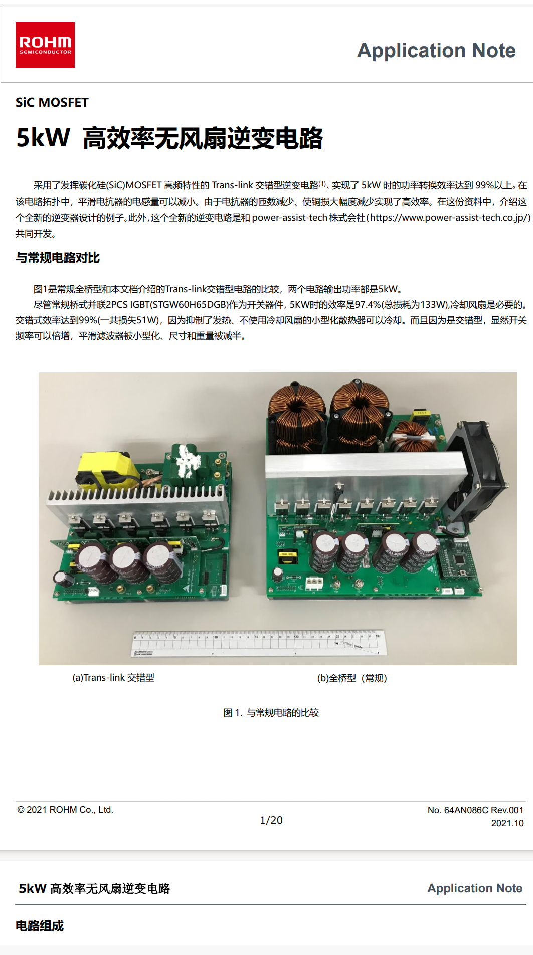
5kW 高效率无风扇逆变电路
采用了发挥碳化硅(SiC)MOSFET 高频特性的 Trans-link 交错型逆变电路(1)、实现了 5kW 时的功率转换效率达到 99%以上。在该电路的拓扑,平滑电感器的电感量可以减小。由于电感器的匝数减少、使功损大幅度减少实现了高效率。
这份资料介绍这个全新的逆变器设计例子。此外,这个全新的逆变电路是和 power-assist-tech 株式会社(https://www.power-assist-tech.co.jp/)共同开发。
与常规电路对比图1是常规全桥型和本文档介绍的Trans-link交叉型电路的比较,两个电路输出功率都是5kW。尽管常规桥式并联2PCS IGBT(STGW60H65DGB)作为开关器件,5KW时的效率是97.4%(总损耗为133W),冷却风扇是必要的。
交叉式效率达到99%(一共损失51W),因为抑制了发热、不使用冷却风扇的小型化散热器可以冷却。而且因为是交叉型,开关频率可以倍增,平滑滤波器被小型化、尺寸和重量被减半。

 浙公网安备 33010602011771号