
Xilinx 7 Series FPGA Clocking Overview(From UG472)
时钟架构概述
7系列 FPGA 时钟资源 用专用的全局性的和区域性的 I / O 和时钟资源处理各种时钟需求。
- 全局时钟树可为整个设备范围内(across the device)同步元素提供时钟。
- I / O 和区域(regional)时钟树最多可为三个垂直相邻的时钟区域提供时钟。
CMT:提供时钟频率合成,去偏斜和抖动过滤功能,包含1个MMCM和1个PLL,位于CMT colume,紧邻I/O colume。
每个7系列设备都划分为多个时钟区域(clock region,下同),用于提供时钟。
- 时钟区域的数量和设备尺寸有关,最小的只有1个,最大的有24个。
- 1个时钟区域包括一个区域中的所有同步元素(例如:CLB,I / O,串行收发器,DSP,Block RAM,CMT),该区域涵盖(span)50个CLB和一个I / O bank(50个I / O)。 水平时钟行(HROW,horizontal clock row)在其中心。
- 每个时钟区域从HROW向上涵盖25个CLB,向下涵盖25个CLB,并且在设备的每一侧水平分布。
时钟路由资源概述
每个 I / O bank都含有时钟功能的输入引脚,可将用户时钟接入7系列FPGA时钟路由资源。 结合专用时钟缓冲器,具有时钟功能的输入可将用户时钟传递至:
- 位于同一顶部/底部半边设备的全局时钟线
- 位于相同的I / O bank和垂直相邻的I / O bank的I / O时钟线
- 同一时钟区域内和垂直相邻时钟区域内的区域时钟线
- 同一时钟区域内的CMT,以及垂直相邻的时钟区域(有限制)
每个7系列单片器件都有32条全局时钟线,它们可以向整个设备中的所有时序资源(sequential resources)提供时钟和控制信号。全局时钟缓冲器(BUFGCTRL,简称BUFG)驱动全局时钟线,并且必须用于访问全局时钟线。 每个时钟区域通过12条水平时钟线,最多可支持这些全局时钟中的12个时钟线。
BUFG有以下特点:
- 能够用作时钟使能电路,用于使能/禁能跨越多个时钟区域的时钟
- 能够用来做无干扰多路复用器
- 选择两个时钟源中的一个
- 从失败的时钟源切换
- 常由CMT驱动,用于
- 消除时钟分发延时
- 调整相关联时钟的延时
水平时钟缓冲(BUFH/BUFHCE)通过HROW可以访问单个时钟区域内的全局时钟线。也可以用作时钟使能电路(BUFHCE),用来单独使能/禁能单个时钟区域内的时钟。每个时钟区域通过12条水平时钟线,最多可支持12个时钟。
每个7系列 FPGA 区域性和 I / O 时钟树可以向整个设备中的所有时序资源(sequential resources)提供时钟。多时钟区域缓冲器(multi-clock region buffers,BUFMR)允许区域性和 I / O 时钟跨越上至3个垂直相邻的时钟区域。
- I / O 时钟缓冲(BUFIO)驱动 I / O 时钟树,提供了对同个 I / O bank 内的顺序 (sequential) I / O 资源的访问。
- 区域性时钟缓冲(BUFR)驱动区域时钟树,后者驱动同个时钟区域内的时钟终点(clock destination),而且通过编程可以用于给输入时钟分频。
- 结合IOB(I / O bank?)内的可编程串行器/解串器(参考UG471,《7 Series FPGAs SelectIO Resources User Guide》),BUFIO 和 BUFR允许源同步系统不添加任何额外逻辑的情况下跨越整个时钟域。
- 与相关的BUFR或BUFIO一起使用时,可以用 BUFMR 驱动相邻区域和 I / O bank 的区域性和 I / O 时钟树。
- 1个时钟区域或 I / O bank 可以支持上至4个唯一 I / O 时钟和4个唯一区域时钟。
高性能时钟路由通过非常低的抖动,最小占空比失真的直接路径将CMT的某些输出连接到I / O。
CMT概览
每个7系列 FPGA 拥有上至24个CMT,每个包含一个 MMCM 和 一个 PLL。MMCM 和 PLL 用于为宽范围的频率做频率合成,也作为内部或外部,以及去偏时钟的抖动过滤器。PLL包含MMCM的一个功能子集。
7系列FPGA时钟输入连接允许多种资源为MMCM和PLL提供参考时钟。
7系列FPGA MMCM在任一方向上都具有无限的精细相移能力,并且可以在动态相移模式下使用。 MMCM在反馈路径或一个输出路径中还具有分数计数器,从而进一步提高了频率合成功能的粒度。
7系列FPGA可以使用LogiCORE™ IP clocking wizard工具,由MMCM 和 PLL构建时钟网络。
时钟缓冲,管理,路由
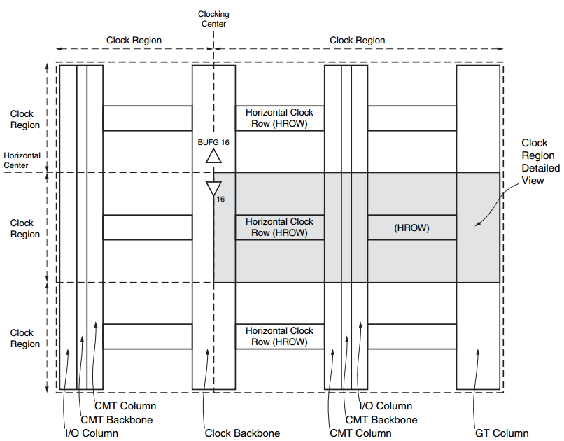
图 7系列FPGA高层时钟架构一览
在上图中,垂直时钟中心线(clock backbone)将设备划分为相邻的左右区域,水平时钟中心线将区域划分为顶部和底部两边。
Clock backbone 的资源镜像映射到水平相邻的左右两个区域,因此也将时钟资源扩展给它们。
顶部和底部将BUFG划分为2组,并加了如何连接的限制。不过BUFG不属于时钟区域,而且可以到达设备上的任何一个时钟点。
HROW 的中心包含了所有水平时钟资源,非区域性时钟资源包含在clock backbone或者CMT backbone里。
一个时钟区域总是包含每列50个CLB,即每列10个36K BRAM,每列20个DSP slice,以及12个BUFH。如果适用的话(?),一个时钟区域包含一个CMT,一个 I / O bank (50个 I / O),1个GT quad(由4个串行收发器组成),以及BRAM column中用于PCIe的半列。
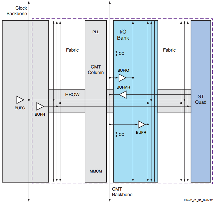
图 时钟区域内可用的时钟资源以及基础连接概览
BUFG 通过 HROW 可以驱动任何区域,即使物理位置并不在那儿。
BUFH 通过 HROW 驱动驱动区域内的任何时钟点。
BUFG 和 BUFH 共享 HROW 的路由路径。
BUFIO 和 BUFR 位于I / O bank内。BUFIO 仅驱动 I / O 时钟资源,BUFR 可用于驱动 I / O资源和逻辑资源。
BUFMR 使能了 BUFIO 和 BUFR 的多区域链接。
有时钟功能的输入(管脚)将外部时钟连接至设备时钟资源。
某些资源可以通过 CMT backbone 连接至上面或下面的区域。
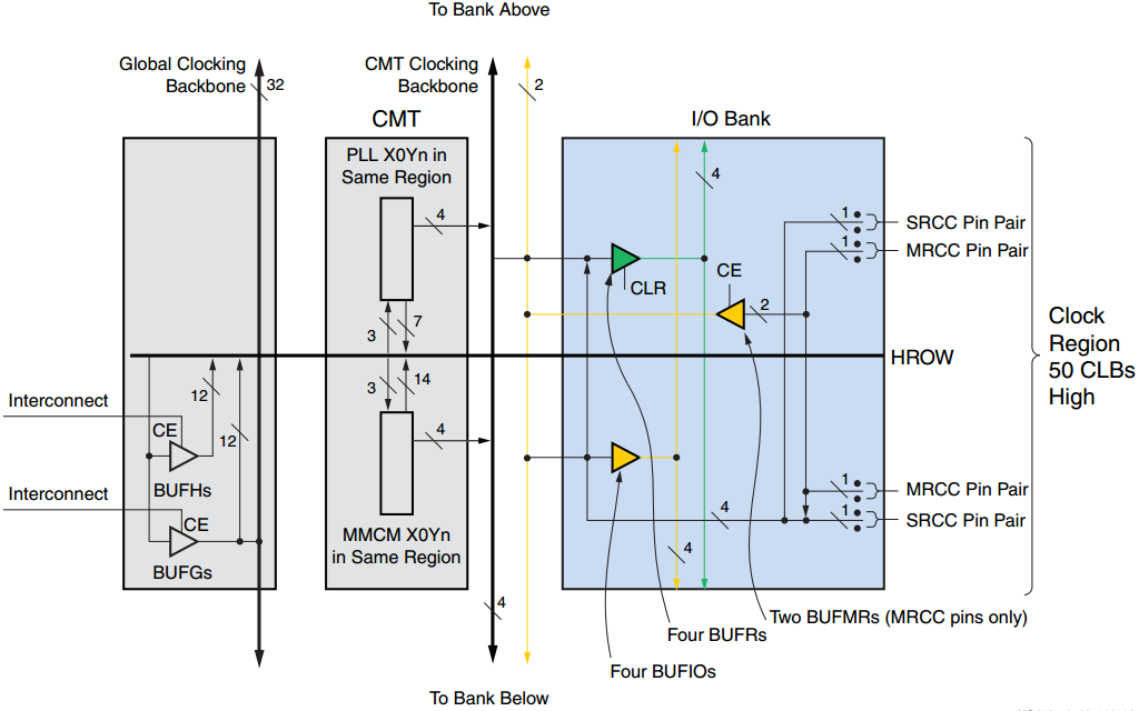
图 单个时钟区域(设备右侧)更详细的视图
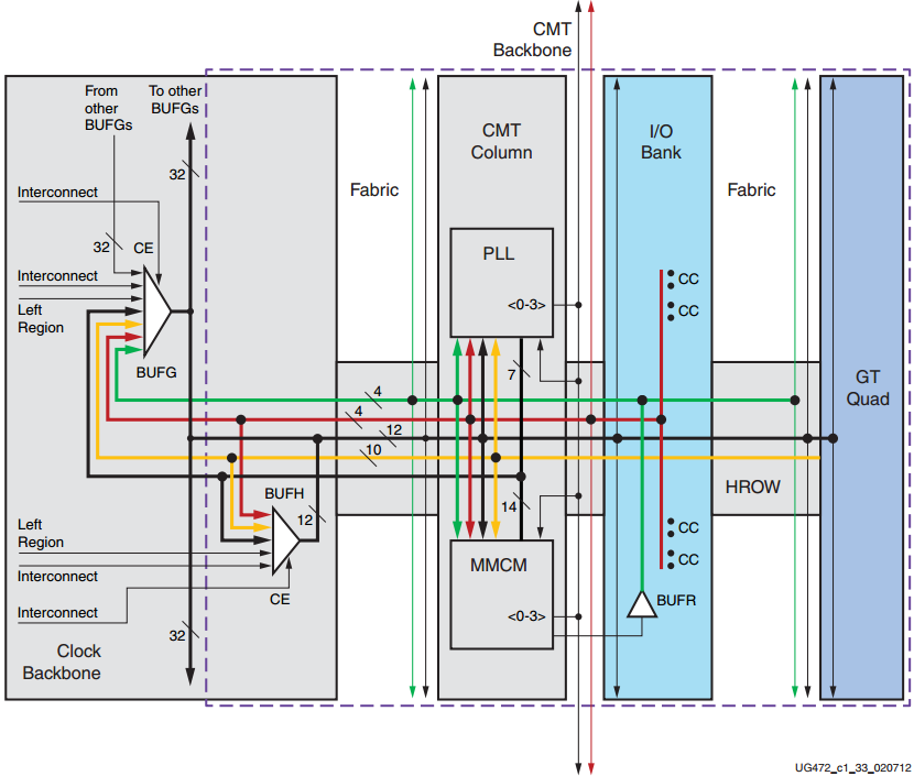
图 BUFG/BUFH/CMT 时钟区域细节
任意1个有时钟功能的输入管脚都能驱动 CMT 中的 PLL / MMCM 以及 BUFH。
BUFG 在图中看起来是位于区域内的,但它的物理位置实际上可以位于 clock backbone 上的其他地方。
BUFG 和 BUFH 共享 HROW 中的12条路由路径,且都能驱动区域内的所有时钟点。
BUFG 还能驱动 BUFH(未显示在图中)。这样在其他情况下在全局时钟分配上可以启用单独的时钟使能(CE)。
GT Quad具有十个专用路径,用来驱动时钟主干中的CMT和时钟缓冲器。
I / O bank 内的BUFR 有4条路径用于驱动逻辑时钟点、CMT 和 BUFG。
CMT使用 CMT backbone 可以(有限制地)驱动邻近区域的 CMT;有时钟功能的管脚可以(有同样限制地)驱动邻近区域的 CMT。
有时钟功能的管脚可以驱动设备同一边(顶部或底部)的 BUFG。
CMT backbone 中有4个路径用来支持垂直区域间的连接。
来自一个时钟区域的时钟源可以驱动自己的和水平相邻的时钟区域的时钟缓冲器。
CMT,有时钟功能的管脚和串行收发器可以通过 BUFH 驱动水平邻近区域,也可以连接到设备同一边(顶部或底部)的 BUFG。
逻辑互连驱动 BUFG 和 BUFH 的 CE 引脚,也可以将时钟驱动到同一缓冲区,但必须注意,因为时序不可预测。
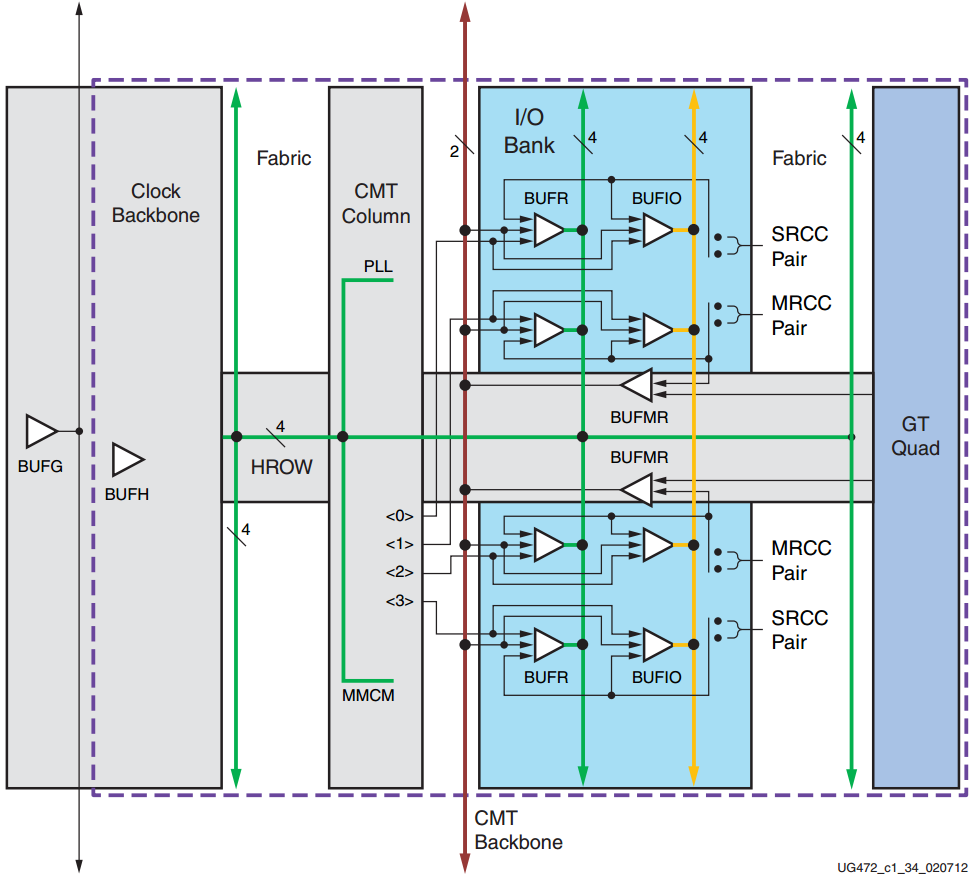
图 BUFR/BUFMR/BUFIO 时钟区域细节
每个 I / O bank 包含4个 BUFIO 和 4个 BUFR。这些缓冲器能够由有时钟功能的管脚驱动,或直接由 MMCM 的特定输出时钟驱动。
一对具有时钟功能的输入引脚称为 MRCC,支持多区域时钟方案。
1个 MRCC 管脚对可以驱动特定的 BUFMR,继而 BUFMR 可以驱动同个或相邻区域的 BUFIO 和 BUFR。同样地,GT quad也能驱动BUFMR。
MMCM <3:0>输出具有通往 BUFR 和 BUFIO 的专用高性能差分路径。 此功能也称为高性能时钟(HPC)。
每个7系列FPGA在器件的左边缘至少有一个完整的I / O列。GT(Gigabit Transceiver)可以是FPGA支持的任意的收发串行收发器(GTP,GTX,或GTH)。支持 GT 的设备在其右边缘要么有一个 GT 和 I / O 的混合列(某些 Kintex-7 和某些 Artix-7),要么右边缘有一个完整的GT列,右侧还有一个完整的 I / O 列(某些 Kintex-7 和某些 Virtex-7)。其他 Virtex-7在左右边缘各有一个 GT 列,在左右侧各有一个完整的 I / O 列。Artix-7 200T 在顶部和底部靠近 Clocking 列的地方有 GTP 收发器。
时钟连接总结
|
Clocking Function or Pin |
Directly Driven By |
Used to Directly Drive |
|
Multi-region clock-capable I/O (MRCC) There are two pin/pairs in each bank. |
External Clock |
MRCCs that are located in the same clock region and on the same left/right side of the device drive: • Four BUFIOs • Four BUFRs • Two BUFMRs • One CMT (one MMCM and one PLL) • CMTs above and below (using limited CMT backbone resources)(1). MRCCs within the same half top/bottom drive: • 16 BUFGs MRCCs within the same horizontally adjacent clock regions drive: • BUFHs |
|
Single-region clock-capable I/O (SRCC) There are two pin/pairs in each bank. |
External Clock |
SRCCs that are located in the same clock region and on the same left/right side of the device drive: • Four BUFIOs • Four BUFRs • One CMT (one MMCM and one PLL) • CMTs above and below (using limited CMT backbone resources)(1). SRCCs within the same half top/bottom drive: • 16 BUFGs SRCCs within the same horizontally adjacent clock region drive: • BUFHs |
|
BUFIO |
Within the same clock region, BUFIOs are driven by: • MRCCs (dedicated 1:1) • SRCCs (dedicated 1:1) • MMCM.CLKOUT0– MMCM.CLKOUT3 • CLKFBOUT • BUFMRs in the same clock region and clock regions below and above |
When used within the same clock region, BUFIOs drive: • ILOGIC.clk • ILOGIC.clkb • OLOGIC.clk • OLOGIC.clkb • OLOGIC.oclk • OLOGIC.oclkb |
|
BUFR |
Within the same clock region, BUFRs are driven by: • MRCC • SRCC • MMCM.CLKOUT0- MMCM.CLKOUT3 • CLKFBOUT • BUFMR from the clock region above and below • General interconnect |
When used within the same clock region, BUFRs drive: • CMT • Any clocking point in the same clock region the BUFG can drive When used within the same half top/bottom, BUFRs drive: • 16 BUFGs (not recommended) |
|
BUFMR |
Within the same clock region, BUFMRs are driven by: • MRCCs (dedicated 1:1) • GT clock outputs listed in this table (see GT Transceiver Clocks) • Interconnect (not recommended) |
When used within the same clock region and the clock regions above and below, BUFMRs drive: • BUFIOs • BUFRs |
|
BUFG |
Within the same top/bottom half, BUFGs are driven by: • SRCCs • MRCCs • CMTs • GT clock outputs listed in this table (see GT Transceiver Clocks) • BUFRs (not recommended) • Interconnect (not recommended) • Adjacent BUFG in the same top/bottom half |
• CMT • GT clock outputs listed in this table (see GT Transceiver Clocks:) • Adjacent BUFGs in same top/bottom half • Any clocking point in the fabric and I/O • CLB control signals • BUFH |
|
BUFH |
Within the same clock region and the horizontally adjacent clock region, BUFHs are driven by: • SRCC • MRCC • CMT • BUFG • GT clock outputs listed in this table (see GT Transceiver Clocks) • Interconnect (not recommended) |
When used within the same clock region, BUFHs drive: • CMT • GT clock outputs listed in this table (see GT Transceiver Clocks:) • Any clocking point in the same clock region the BUFG can drive |
|
GT Transceiver Clocks RXUSRCLK RXUSRCLK2 TXUSRCLK TXUSRCLK2 |
• Any BUFG Within the same clock region, GTs are driven by: • BUFH |
N/A |
|
GT Transceiver Clocks: RXOUTCLK TXOUTCLK |
N/A |
• BUFG within the same half top/bottom When used within the same clock region, GTs can drive: • CMT • BUFMR • BUFH and BUFH in the horizontally adjacent clock region |
|
MGTREFCLK0/1P MGT positive differential reference clock pins MGTREFCLK0/1N MGT negative differential reference clock pins |
External GT reference clock |
• GT reference clock • BUFG within the same half top/bottom When used within the same clock region, external GT reference clock pins can drive: • CMT • BUFMR • BUFH and BUFH in the horizontally adjacent clock region |
|
CMT(1) |
• BUFG • SRCC (same and adjacent clock regions) • MRCC (same and adjacent clock regions) • GTs in the same clock region • A BUFR within the same clock region, and the clock region above or below using a BUFMR • MMCM/PLL.CLKOUT0-3 |
• Any BUFG in same top/bottom half When used within the same clock region, CMTs can drive: • BUFIO (MMCM) • BUFR (MMCM) • BUFH and BUFH in the horizontally adjacent clock region • MMCM/PLL (with phase offset if not adjacent) |
|
IDELAYCNTRL.CLK |
• MRCC/SRCC • BUFG • BUFH |
N/A |
|
CCLK pin |
Configuration logic |
Configuration logic |
|
EMCCLK pin |
N/A |
Configuration logic |
|
TCK pin |
N/A |
JTAG configuration logic and Boundary Scan |

 浙公网安备 33010602011771号