Verilog Circuits-Sequentiial Logic-Shift Registers
Problem 106:4-bit shift register
设置一个 4bit 异步复位,拥有同步置位和使能的右移移位寄存器
- areset:寄存器复位为 0
- load:将 data[3:0]输入至移位寄存器中
- ena:使能信号控制向右移动,(q[3]q[2]q[1]q[0] ---> 0q[3]q[2]q[1],q[0]在移动后消失了,原先 q[3]的位置变为 0)
- q : 移位寄存器中的数据
如果 ena 和 load 同时为高,load 有更高的优先级。
module top_module(
    input clk,
    input areset,  // async active-high reset to zero
    input load,
    input ena,
    input [3:0] data,
    output reg [3:0] q);
    always @(posedge clk or posedge areset)//异步复位
        begin
            if(areset)
                q<=4'b0;
            else if(load)
                q<=data;
            else if(ena)
                begin
                    q[3:0]<={1'b0,q[3:1]};
                end
        end

endmodule
Problem 107:Left/right rotator
设计一个 100bit 的可左移或右移的移位寄存器,附带同步置位和左移或右移的使能信号。
本题中,移位寄存器在左移或者右移时,不同于 Problem106 的补 0 和直接舍弃某一 bit 位,本题是要求在 100bit 内循环移动,不舍弃某一 bit 位同时也不补 0
比如说右移 1bit,在 Problem106 就是补 0 和丢弃 q[0]。而在本题中右移 1bit 为{q[0], q[99:1]}
- load:load 信号将 data[99:0] 输入至寄存器内。
- ena[1:0] 信号选择是否移位和移位的具体方向
- 2'b01 右移一位
- 2'b10 左移一位
- 2'b00 和 2'b11 不移动
- q:移位后寄存器内的数据
module top_module(
    input clk,
    input load,
    input [1:0] ena,
    input [99:0] data,
    output reg [99:0] q);
    always @(posedge clk)
        begin
            if(load)
                q<=data;
            else if(ena==2'b01)
                q<={q[0],q[99:1]};
            else if(ena==2'b10)
                q<={q[98:0],q[99]};
            else
                q<=q;
        end
endmodule
Problem 108:Left/right arithmetic shift by 1 or 8
设计一个 64bit 带同步置位的算术移位寄存器,该寄存器可以由 amount 控制来移动方向和每次移动的次数
- 算术右移移位寄存器中的符号位(q[63])移位,不像是逻辑右移中进行补零的操作,而是保留符号位后再进行补位
一个 5-bit 值为 11000 的寄存器算术右移一位后为 11100, 而逻辑右移后为 01100。
同样的,一个 5-bit 值为 01000 的寄存器算术右移一位后为 00100,且该寄存器逻辑右移会产生同样的结果。
-
load:置位信号
-
ena : 使能信号,来选择是否移位
-
amount : 选择移位的方向和移位的个数
- 2'b00 : 左移 1bit
- 2’b01 : 左移 8bit
- 2'b10 : 右移 1bit
- 2'b11 : 右移 8bit
-
q : 寄存器中的数据
module top_module(
    input clk,
    input load,
    input ena,
    input [1:0] amount,
    input [63:0] data,
    output reg [63:0] q);

    always @ (posedge clk)
        begin
            if(load)
                q <= data;
            else if (ena)
                begin
                    case(amount)
                        2'b00 :     begin
                            q <= {q[62:0], 1'b0};
                        end

                        2'b01:  begin
                            q <= {q[55:0], 8'b0};
                        end

                        2'b10: begin
                            q <= {q[63], q[63:1]};
                        end

                        2'b11: begin
                            q <= {{8{q[63]}}, q[63-:56]};
                            //算术右移是用符号位填充和q的高56位
                            //{{8{q[63]}}, q[63-:56]}
                        end
                    endcase
                end
        end

endmodule
Problem 109 :5-bit LFSR
线反馈移位寄存器,指通常带有几个 XOR 门来产生下一状态的移位寄存器。
Galois LFSR 是一个特殊的移位寄存器,其中带有 “tap”位的位置与输出位 XOR 产生下一个值没有“tap”位标志的正常移位。如果“tap”位置经过仔细选择后,LFSR 将设置为最大长度。再重复之前 LFSR 的最大长度为 \(2^n-1\)
下图所示 LFSR 为在位置 5 和位置 3 包含"tap"位的 5-bit 最大长度 LFSR。开始为位置 1,输入为 0。
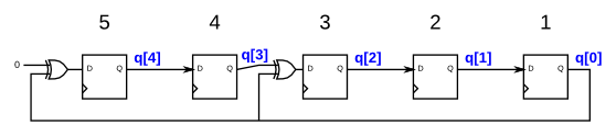
设计如上图所示 LFSR,复位信号使 LFSR 复位为 1.
module top_module(
    input clk,
    input reset,    // Active-high synchronous reset to 5'h1
    output [4:0] q
);
    always @ (posedge clk)
        begin
            if(reset)
                q <= 5'b00001;
            else
                begin
                    q[4] <= 1'b0 ^ q[0];
                    q[3] <= q[4];
                    q[2] <= q[3] ^ q[0];
                    q[1] <= q[2];
                    q[0] <= q[1];
                end
        end

endmodule
- 该寄存器类似于一种伪随机数生成器,相比普通的多级寄存器组,区别在于部分寄存器的输入经过一个异或逻辑
Problem 110:3-bit LFSR

使用 Verilog 实现上图中的时序电路,假设你要在 DE1-SoC 教学板上实现这个电路,将输入端口 r 连接到板子上的拨动开关,clock 端口接到按键 KEY[0],端口 L 接到按键 KEY[1]。输出端口 Q 连接到板子上的红色 LED。
- 本题原理与上一题相同,但加入了一个板子和其外部接口
module top_module (
	input [2:0] SW,      // R
	input [1:0] KEY,     // L and clk
	output reg [2:0] LEDR);  // Q

    wire clk = KEY[0];
    wire l = KEY[1];
    wire [2:0] d = l?SW:{LEDR[1]^LEDR[2],LEDR[0],LEDR[2]};

    always @(posedge clk)begin
            LEDR	<=	d;//不懂这边的d是啥
    end

endmodule
Problem 111:32-bit LFSR
参考 109 题中的 5bit LFSR,实现一个 32bit 的 LFSR,抽头点为 32,22,2,1.
- 抽头点
- problem109 的抽头点为 5 和 3,也就是第五个和第三个触发器经过了异或逻辑
- 那么本题就是第 32,22,2,1 个寄存器的输入经过了异或逻辑
- q[21] <= q[22]^q[0]
- q[1] <= q[2]^q[0]
- q[0] <= q[1]^q[0]
- q[31]<=q[0]^1'b0 即为输入端,所以相当于输入 q[0]本身
- q[31-:9]表示从 q[31]开始的 9 个 bit
module top_module(
    input clk,
    input reset,    // Active-high synchronous reset to 32'h1
    output [31:0] q
);
    always @(posedge clk)
        begin
            if(reset)
                q<=32'd1;
            else
                begin
                    q<={q[0],q[31:22],q[22]^q[0],q[20:3],q[2]^q[0],q[1]^q[0]};//相当于先进行了右移,然后将输入换成异或逻辑
                end
        end


endmodule
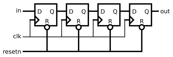
Problem 112:Shift Register
实现如图电路
module top_module (
    input clk,
    input resetn,   // synchronous reset
    input in,
    output out);
reg q0,q1,q2;
    always @(posedge clk)
        begin
            if(!resetn)
                begin
                    q0<=1'b0;
                    q1<=1'b0;
                    q2<=1'b0;
                    out<=1'b0;
                end
            else
                begin
                    q0<=in;
                    q1<=q0;
                    q2<=q1;
                    out<=q2;
                end
        end
endmodule
- official solution
module top_module (
	input clk,
	input resetn,
	input in,
	output out
);

	reg [3:0] sr;

	// Create a shift register named sr. It shifts in "in".
	always @(posedge clk) begin
		if (~resetn)		// Synchronous active-low reset
			sr <= 0;
		else
			sr <= {sr[2:0], in};
	end

	assign out = sr[3];		// Output the final bit (sr[3])

endmodule
Problem 113:Shift Register
实现下图中的 n bit 移位寄存器电路,这题希望使用例化的方式,例化 4 个选择器 + 触发器模块实现一个 4bit 移位寄存器。另外还要进行一些连线工作。

- Connect the R inputs to the SW switches,
- clk to KEY[0] ,
- E to KEY[1] ,
- L to KEY[2] , and
- w to KEY[3] .
- Connect the outputs to the red lights LEDR[3:0] .
module top_module (
    input [3:0] SW,
    input [3:0] KEY,
    output [3:0] LEDR
); //
    wire [3:0]w_input={KEY[3],LEDR[3],LEDR[2],LEDR[1]};//每个阶段的输入不一样
    generate
        genvar i;
        for(i=0;i<4;i++)
            begin:muxdff
    MUXDFF shift1(.clk(KEY[0])
                  ,.E(KEY[1])
                  ,.R(SW[i])
                  ,.L(KEY[2])
                  ,.w(w_input[i])
                  ,.Q(LEDR[i])
                 );
            end
    endgenerate
endmodule

module MUXDFF (input clk,input E,input R,input L,input w,output Q);
      wire d;
    wire d_in;
    reg Q_out;			//寄存器变量
    assign d=E?w:Q;
    assign        d_in=L?R:d;
    always @(posedge clk)
        begin
          Q_out<=d_in;		//时钟

        end

assign Q=Q_out;			//组合赋值
endmodule
Problem 114 Shift Register(Exams/m2014 q4k)
设计一个 8*1 结构的存储体电路。存储的输入通过移入比特进行,读取类似于传统 RAM 中的随机读取,即可以指定读出比特的位置,通过 3 个输入端口指定读取位置。
首先通过 8 个触发器实现一个 8bit 深的移位寄存器。8 个寄存器的输出依次为 Q[0]...Q[7]。
移位寄存器的输入为 S,输入首先会填充到 MSB(最高位),Q[0]。
enable 信号控制是否移位,电路还有三个额外的输入 ABC,和一个输出 Z
工作的功能如下:当 ABC = 000 时,Z = Q[0],当 ABC = 001 时,Z = Q[1],以此类推。你的电路中只能包括一个 8bit 移位寄存器以及一个多路选择器。(这就是个三输入查找表 LUT 电路)
module top_module (
	input clk,
	input enable,
	input S,

	input A, B, C,
	output reg Z
);

	reg [7:0] q;

	// The final circuit is a shift register attached to a 8-to-1 mux.


	// Create a 8-to-1 mux that chooses one of the bits of q based on the three-bit number {A,B,C}:
	// There are many other ways you could write a 8-to-1 mux
	// (e.g., combinational always block -> case statement with 8 cases).
	assign Z = q[ {A, B, C} ];


	// Edge-triggered always block: This is a standard shift register (named q) with enable.
	// When enabled, shift to the left by 1 (discarding q[7] and and shifting in S).
	always @(posedge clk) begin
		if (enable)
			q <= {q[6:0], S};
	end


endmodule

 浙公网安备 33010602011771号