Glitch free safe clock switching
Glitch free safe clock switching
From: http://www.vlsi-world.com/content/view/64/47/1/2/
Safe and Glitch free clock switching
Digital circuits are often running in different clock domains. In many circumstances the clock of these circuits need to be switched while the logic (circuit) is running. The clock switching can be done in analog circuit or in digital circuit. The Implementations in this page give details of clock switching digitally. The simplest way of clock switching can be done with simple multiplexers.
Simple clock switch
Two clocks are multiplexed and selected by a signal which is generated from the internal logic. The following circuit shows the clock switching using a multiplexer. Above circuit can be described in Verilog as follows.

In the above circuit when select is ‘1’ clk_b forwarded to the output and when select is ‘0’ clk_b forwarded to the output. The switching of these clock are combination to the select signal that is selects signals immediately (on-the-fly) switches the clock with out respect of the state of the both clocks. This is not safe some time, like the following simulation of the above circuit.

The simulation output shows a Glitch on the clock path. It is due to the ‘select’ signal goes up just before the clk_b is going down. These glitches are very hazardous for any circuits. If the width of the glitch is too small they are sensed by some flip-flops and some will not. Due to this problem the output of the complete circuit is undetermined. These glitches are also leads into Metastability problems. Since glitches are very short pulses it may violate the setup and hold time of the flip-flops and output of these flip-flops are in quasi state (outputs are not determined as ‘1’ or ‘0’). Verilog realization of proceeded circuit follows.
 `timescale 1ns/10ps
2
 module clk_switch (
3
 // Outputs
4
 out_clk,
 5
 // Inputs
 6
 clk_a,
7
 clk_b,
8
 select );
 9
 input clk_a;
 10
 input clk_b;
 11
 input select;
 12
 output out_clk;
 13
 reg out_clk;
14
 always @ (select or clk_a or clk_b)
15
 begin
begin 16
 if select == 1)
 17
 out_clk <= clk_a;
 18
 else
else 19
 out_clk <= clk_b;
20
 end
end21
 endmodule
Glitch free safe clock switch implementation
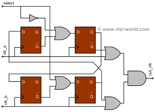
The logic is little complex than the simple clock switch, the clock switching will not happen immediately after switching the select signal. This circuit allows both clock settle down and switches the new clock to the circuit. It eliminates glitch or spikes in the clock signal. The safe clock switch circuit is implemented as in the following diagram.

Following figure shows the simulation of glitch free safe clock switch. For both implementations same test bench is used. Code for the test bench is available at end of the article.

Above circuit works well with related and unrelated clock. Related clocks means both clocks come from the same clock source (they are in phase) un-related clocks (they are not in the phase) are not come from the same clock source.
In this implementation the select signal registered it makes sure that the there will not be any change in the output while both clocks are high. First stage flip-flops remove the meta-stability problem. Verilog implementation for glitch free clock switch.
 `timescale 1ns/100ps
2
 module clk_switch (
3
 // Outputs
4
 out_clk,
5
 // Inputs
6
 clk_a, clk_b, select
7
 );
);8

9
 input clk_a;
10
 input clk_b;
11
 input select;
12

13
 output out_clk;
14
 wire out_clk;
15

16
 reg q1,q2,q3,q4;
17
 wire or_one, or_two,or_three,or_four;
18

19
 always @ (posedge clk_a)
20
 begin
begin21
 if (clk_a == 1'b1)
22
 begin
begin23
 q1 <= q4;
24
 q3 <= or_one;
25
 end
end26
 end
end27

28
 always @ (posedge clk_b)
29
 begin
begin30
 if (clk_b == 1'b1)
31
 begin
begin32
 q2 <= q3;
33
 q4 <= or_two;
34
 end
end35
 end
end36

37
 assign or_one = (!q1) | (!select);
38
 assign or_two = (!q2) | (select);
39
 assign or_three = (q3) | (clk_a);
40
 assign or_four = (q4) | (clk_b);
41

42
 assign out_clk = or_three & or_four;
43

44
 endmodule
 TestBench
 `timescale 1ns/10ps
2

3
 module tb_clk_switch;
4

5
 reg clk_a;
6
 reg clk_b;
7
 wire out_clk;
8

9
 reg select;
10

11
 initial
12
 begin
begin13
 select <= 1'b0;
14
 clk_a <= 1'b1;
15
 clk_b <= 1'b1;
16
 #87.2
#87.217
 select <= 1'b1;
18
 #81.9
#81.919
 select <= 1'd0;
20
 #50
#5021
 $stop;
22
 end
end23

24
 always #5.7 clk_a = ~clk_a;
25
 always #2.5 clk_b = ~clk_b;
26

27
 clk_switch ins1 (
28
 .clk_a(clk_b),
29
 .clk_b(clk_a),
30
 .select(select),
31
 .out_clk(out_clk)
32
 );
);33
 endmodule
posted on 2009-11-17 13:42 Homography Matrix 阅读(4057) 评论(0) 收藏 举报


 浙公网安备 33010602011771号