
Marin说PCB之LPDDR5的仿真报告分析--01 - 实践
小编我最近被宗门大长老汪涵安排到南京出差了,这边遇到一个新来的EE同事史大勇让我帮忙给他整理一份关于LPDDR5的仿真报告,并且指出和我们PCB设计上有关系的问题点。
仿真报告如下所示:目前只是做了DQ Write Simulation。
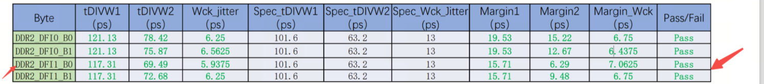
第一可以得出的是K3KLDLD0FM颗粒 DQ Write 6400Mbps 信号仿真结果Pass。 大家能够先对比下面这两组比较差的看下其PCB走线的差别:
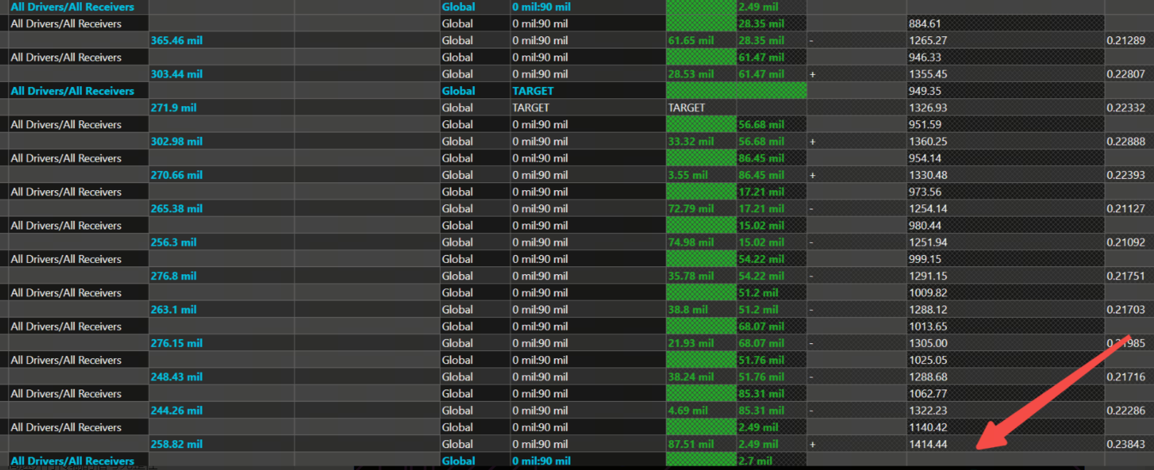
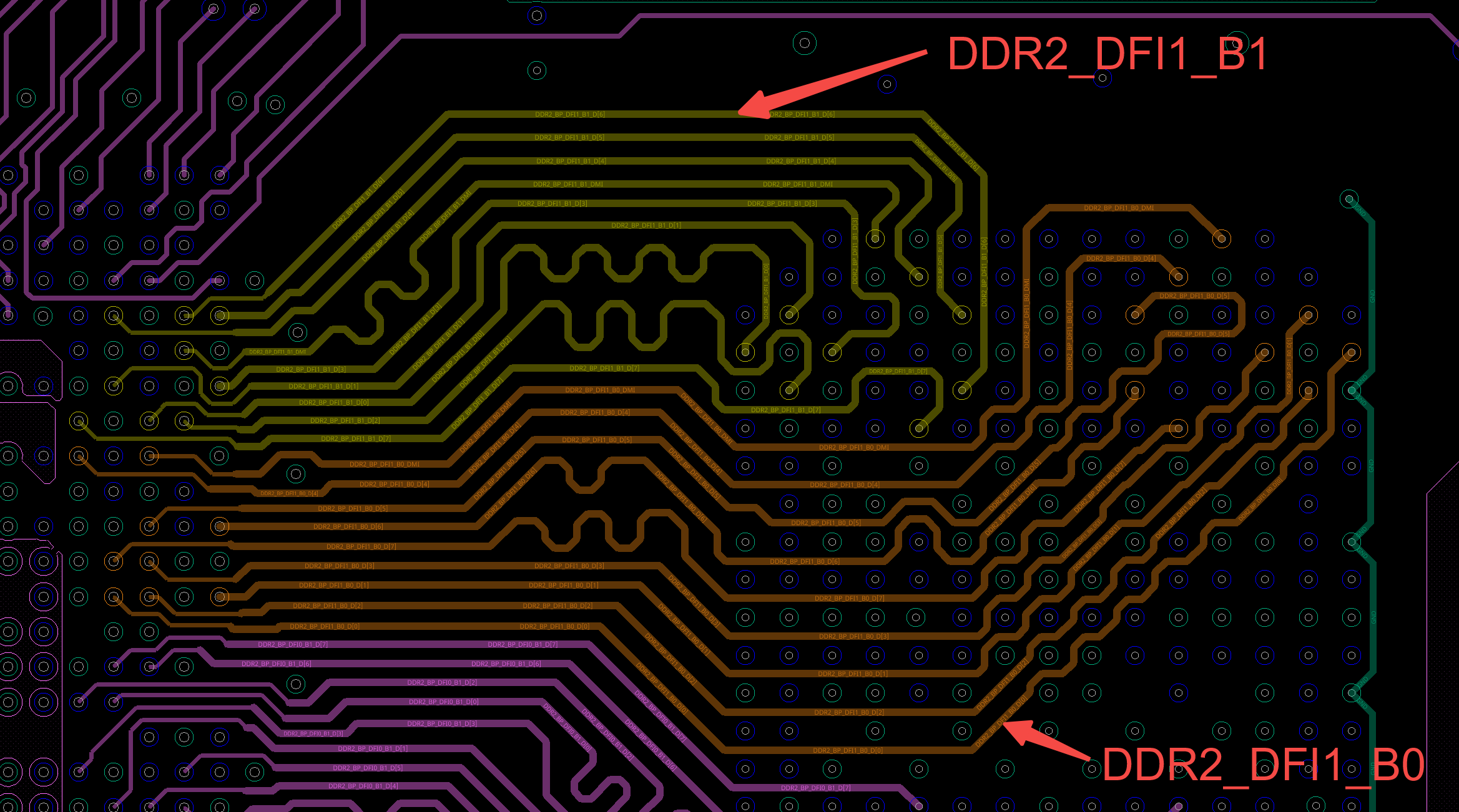
1,走线长度上,DDR2_DFI1_B1这个组数据线最长的为1195MIL,而DDR2_DFI1_B0最长的数据线走线长度为1414MIL。

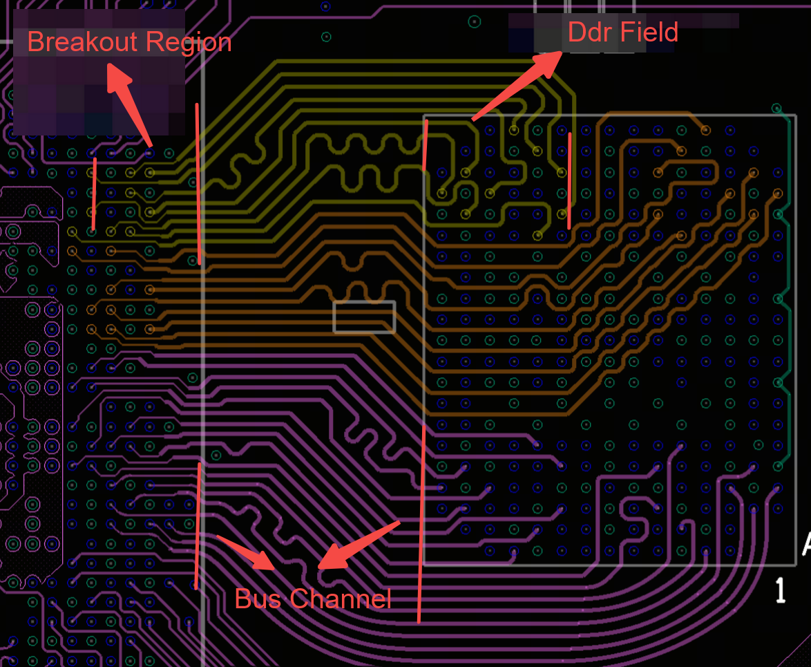
二,正常我们的DDR走线是分布在三个区域内的,Breakout,Bus Channel以及 DRAM Field区域。这三个区域走线间距要求如下所示:
A,Breakout—— the region where signals are fanned out away from the processor. Due to the ball pitch of the processor package, the spacing rules of the signals in this area are relaxed that signals are allowed to be closer to each other.
B,Bus Channel—— the region where signals travel from the processor breakout to the DRAM Field area. While in Bus Channel, the spacing and impedance rules are more stringent. Bus Channel routing rules are specified in terms of a target trace impedance and relative “H” spacing. “H” is a multiple of the dielectric height.
C,DRAM Field——the region where signals are routed to the vias which connect to the DRAM balls. Due to the ball pitch of the DRAM package, the signals are allowed to route with reduced trace width and spacing for a limited length.
依据两组数据线的整体走线分布情况可知DDR2_DFI1_B0这组走线不仅仅是走线长度最长,而且这组BUS走线路径主要分布在了DRAM Field区域了,而不是在我们的Bus Channel这个区域了,因为由于器件封装焊盘的尺寸和焊盘排列疑问,我们的DDR信号在Breakout和DRAM Field区域走线间距无法严格地按照Bus Channel这个区域规则来设置的,因而手册上才会放宽松这两个区域走线的间距要求的。所以说在布线的时候尽量避免在这两个区域走线过长了,尤其是一组数据线的平行走线长度手册要求的是尽量小于100MIL的。
好了,诸位道友们以上就是本期的所有内容了,我们下期文章不见不散。


--------声明:本文属于小编的原创文章,如需转载请注明来源!

 浙公网安备 33010602011771号