
LVDS_33 support
在HR bank/HD bank中,支持LVDS的bank使用VCCO 3.3v供电,仅仅需要对端给过来的信号,满足标准的LVDS差模电压/共模电压的标准即可。如下截图:

限制:
仅能作为input使用,无法作为output。
应用:
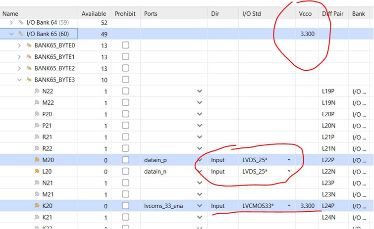
硬件上该bank VCCO接3.3V电压,实际vivado中IO电平标准设置为LVDS_25即可。下图为实际在vivado中验证通过的示例。
原理解释:
LVDS_18 LVDS_25 LVDS_33都仅仅是FPGA侧的称呼,区别就是VCCO电压的区别。对于ASSP/ASIC来说,仅有LVDS的说法。只需要信号特性满足LVDS的要求(主要是input/output的差模/共模电压等指标),互相均可以连接。
3.3V LVDS:
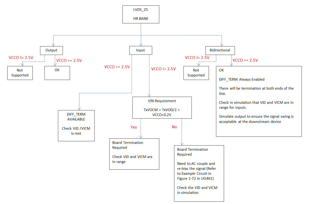
- The "LVDS_33" I/O Standard that was available in some older FPGA families, is not supported in 7 Series, UltraScale or UltraScale+ devices.
- Neither High Range (HR) banks, High Density (HD) banks, nor High Performance (HP) banks can have their VCCO pins powered at 3.3V (if using LVDS outputs).
- Older families' LVDS_33 outputs might be supportable in the 7 Series, UltraScale and UltraScale+ I/O banks, but care must be used to ensure that:
- Vin in Table 1 and 2 of the Data Sheet is not violated.
- VIDIFF and VICM for LVDS (HP banks) or LVDS_25 (HR or HD banks) is not violated.
Running signal integrity simulations using IBIS models might be required in order to insure that those two items are not violated.

 浙公网安备 33010602011771号