

AMD R600 Architecture and GPU Analysis
Published on 14th May 2007, written by Rys for Consumer Graphics - Last updated: 14th May 2007
Introduction
Given everything surrounding the current graphics world at the time of writing -- with big highlights that include the recent AMD/ATI merger, the introduction of a new programming shading model via DirectX, NVIDIA's introduction of G80, real-time graphics hardware in the new generation of consoles, and Intel's intent to come back to discrete -- the speculation and anticipation for AMD's next generation of Radeon hardware has reached levels never seen before. 4 years in the making by a team of some 300 engineers, the chip takes the best bits of R5 and Xenos, along with new technology, to create their next architecture.
How it performs, and how it slides in to the big graphics picture, means the base architecture and its derivative implementations will have an impact on the industry that will be felt a long time from launch day. If you're not excited about what we're about to explain and go over in the following pages, you haven't been paying attention to the state of the GPU union over the last year and a half, since we live in the most exciting graphics-related times since Voodoo Graphics blazed its real-time, mass-market consumer trail.
The engineers at the new AMD Graphics Products Group have been beavering away for the last few years on what they call their 2nd generation unified shader architecture. Based in part on what you can find today in the Xenos GPU inside the Xbox 360 console, AMD's D3D10 compliant hardware has been a long time coming. Obviously delayed and with product family teething troubles, R600, RV610 and RV630 -- the first implementations of the new architecture -- break cover today for the first time, at least officially!
We'll let you know the architecture basics first, before diving in for closer looks at some of the bigger things the architecture and the implementing GPUs do. As with our G80 analysis, we split things in to three, covering architecture in this piece, before looking at image quality and performance in subsequent articles, to divide things up into manageable chunks for us to create and you to consume.
AMD have embargoed performance analysis of RV610 and RV630 until next month, but we're allowed to talk about those GPUs in terms of architecture and their board-level implementations, so we'll do that later today, after our look at R600, the father of the family. Tank once said, "Damn, it's a very exciting time". Too true, Tank, too true. He also said shortly afterwards, "We got a lot to do, let's get to it". We'll heed his sage advice.
The Chip - R600
-
R600 is the father of the family, outgunning G80 as the biggest piece of mass market PC silicon ever created, in terms of its transistor count. It's not feature identical to the other variations, either, so we'll cover the differences as we get to them.
ATI R600 details
Foundry and process
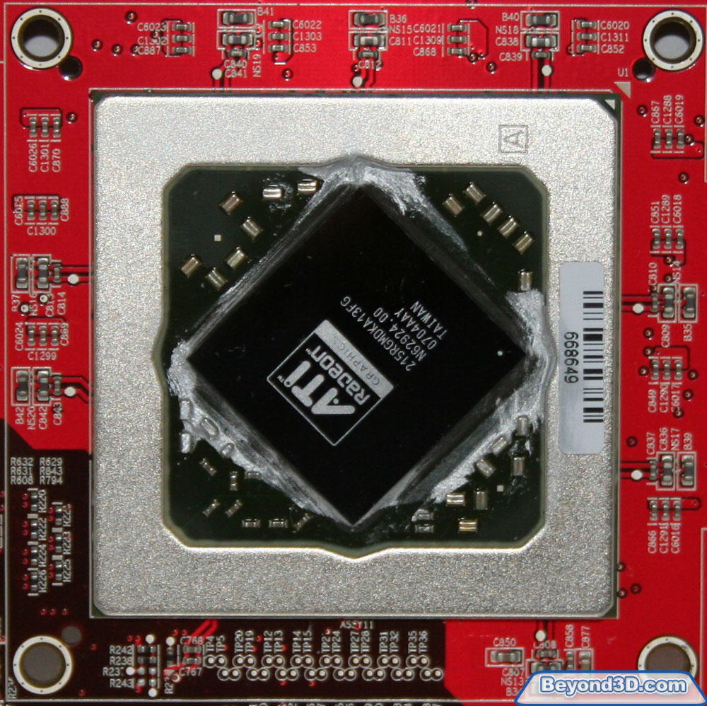
80nm @ TSMC, 720M
Die Size
420mm²
20mm x 21mm
Chip Package
Flipchip
Basic Pipeline Config
16 / 16 / 32
Textures / Pixels / Z
Memory Config
512-bit
8 x 64-bit
API Compliance
DX10.0
System Interconnect
PCI Express x16
Display Pipeline
Dual dual-link DVI, HDCP, HDMI
|
ATI R600 details |
|
|---|---|
|
Foundry and process |
80nm @ TSMC, 720M |
|
Die Size |
420mm² |
|
Chip Package |
Flipchip |
|
Basic Pipeline Config |
16 / 16 / 32 |
|
Memory Config |
512-bit |
|
API Compliance |
DX10.0 |
|
System Interconnect |
PCI Express x16 |
|
Display Pipeline |
Dual dual-link DVI, HDCP, HDMI |
-
TSMC are AMD's foundry partner for this round of graphics processors once again, with R600 built on their 80HS node at 80nm. 720M transistors comprise the huge 20x21mm die, which contains all of the logic, including display and signal I/O. R600 is an implementation of AMD's 2nd generation unified shading architecture, fully threaded for computation, data sampling and filtering, and supporting Shader Model 4.0 as set out by Direct3D 10. R600 also sports a hardware tesselation unit for programmable surface subdivision and certain high order surfaces outside of any major existing API, although programmable using them.
-
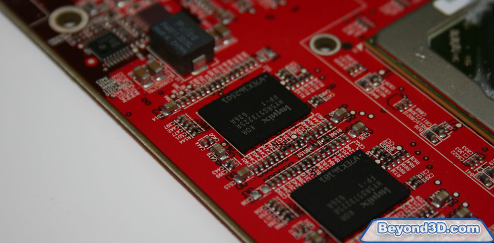
R600 sports a 512-bit external memory bus, interfacing with an internal, bi-directional 1024-bit ring bus memory controller, with support for dozens of internal memory clients and GDDR3 or GDDR4 memories for the external store. Sticking with memory, the R600 architecture is cache-heavy internally, SRAM logic a significant portion of the die area. The external bus interface to the PC host is PCI Express, access to that coming via dedicated stop on the internal rings.
R600 sports AMD's next generation video decoding core, called the Unified Video Decoder or UVD for short. The UVD is designed to handling full H.264 AVC decode processing offload at maximum bitrates for both Blu-Ray and HD-DVD video at maximum resolution. In terms of power management, the chip supports clock throttling, voltage adjust for p-states and entire unit shutdown depending on workload, combined by marketing under the umbrella of PowerPlay 7.
We'll cover all of those things and more as the article(s) progress. The initial R600-based SKU is called Radeon HD 2900 XT, so we'll take a look at the reference board before we move on to the architecture discussion for the chip that powers it. We'll cover RV610 and RV630 separately later today, as mentioned.
The Radeon HD 2900 XT Reference Board
The only R600-based launch product is Radeon HD 2900 XT. To signal the intent of the products in terms of how they're able to process screen pixels, be that in motion video or real-time 3D graphics, AMD are dropping the X from the product family in place of HD. The familiar XT, XTX (maybe) and PRO monikers for inter-family designation will stay, however. Radeon HD 2900 XT sports two clock profiles, the 3D one seeing R600 clocked at 742MHz (the chip has a single master clock domain, across many slightly asynchronous subdomains), with 512MiB of GDDR3 memory clocked at 825MHz. The 2D profile sees things drop to 507MHz for the chip, with the memory run at 514MHz. Windowed applications are run in the 2D clock profile.
|
ATI Radeon HD 2900 XT 512MiB Details |
|
|---|---|
|
Board Name |
Radeon HD 2900 XT |
|
Memory Quantity |
512MiB |
|
Chip |
|
|
Core Frequency |
742MHz |
|
Memory Frequency |
825MHz |
|
Theoretical Performance @ 742/825 |
|
|
Pixel Fillrate |
11872 Mpixels/sec |
|
Texture Fillrate |
11872 Mtexels/sec |
|
Z sample rate |
23744 Msamples/sec |
|
AA sample rate |
47488 Msamples/sec |
|
Geometry rate |
742 Mtris/sec |
|
Memory Bandwidth |
105.6 GB/sec |
The table above will start to give some of the story away if you're willing to take the base clock and do some basic arithmetic. By virtue of the 512-bit external memory bus and Hynix HY5RS573225A FP-1 DRAM devices clocked at 825MHz (1.65GHz effective rate), HD 2900 XT has a peak theoretical bandwidth of 105.6GB/sec. One hundred and five point six, for those still blinking at the figure in numerical form. And while AMD aren't the first company to deliver a single board consumer solution with a peak bandwidth higher than 100GB/sec, given NVIDIA's soft launch of GeForce 8800 Ultra and its 103.6GB/sec peak via a 384-bit bus, they're definitely the first to try a 512-bit external bus on a consumer product.
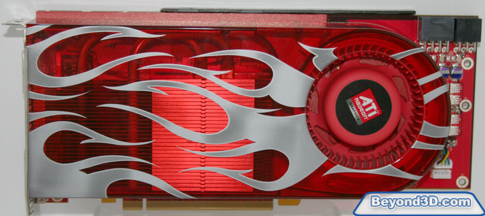
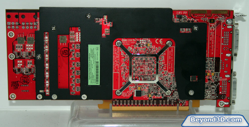
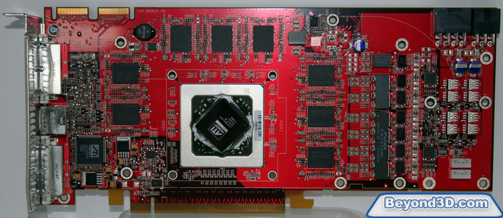

Retail editions of the board are barely larger than AMD's outgoing Radeon X1950 XTX, PCB size wise, although the cooler is a good bit beefier. While it looks like your average double slot cooler for a high end board, replete with blower fan and rear exit for the exchanged heat, the mass of the sink attached to the board and the components it's cooling is significant. In fact, the board is the heaviest 'reference' hardware yet created, with reference used to define the cooler that the IHV officially specifies.
It's a somewhat sad fact, for AMD and the consumer, that TSMC's 80HS process has pretty horrible static power leakage properties. Given the process properties, the die area, clocks for GPU and mem, and the memories themselves, it's no honest surprise to see the fastest launch board based on R600 coming with such a cooler. It's also no real surprise to see it come with a pair of external power input connectors, and one of those is the new 8-pin variant as well. That version of the connector gives the board another +12V input source at just over 6A max current.
The board doesn't require you fill that connector block up with power-giving pins, though, since it runs happily with a regular pair of 6-pin inputs. Look closely and you'll see the 8-pin block holds the 6-pin block, and there's only one orientation that can make it happen, so you don't connect the wrong pins and have things go horribly wrong.
A pair of dual-link DVI connectors dominates the backplane space that the first slot occupies, with the grille for the heat output dominating the second. The DVI ports (although it's unclear if it's just one of them or both) support HDMI output for video and audio via a supplied active convertor. It appears that audio is either muxed into the video bitstream pushed out over the pins, or the spare pins on the dual-link connector (the version of HDMI that the hardware supports is analogous to single-link DVI for the video portion) are used for that, but it's an implementation detail at best.
Physicals

In terms of the board's physical properties when being used in anger, we've run our test sample just fine using a PSU that provides only 6-pin connectors. Calibrating against other boards on the same test platform, we estimate (because we're not 100% certain about other board's peak power either) peak load power from the board, at least using our load condition of 3DMark05's GT3 @ 1920x1200 w/4xAA/16xAF, of less than 200W at stock frequencies. We haven't tried overclocking enough to be sure of a peak power draw using the Overdrive feature.
Using AMD's GPU overclocking tool which is able to read the GPU's thermal diode, load temperatures for the GPU approach 90°C with our sample. Under the load condition generating that heat, the fan speed is such that board volume is higher than any of the board boards on test, and that the pitch of the noise is annoyingly high with a whistling property to it, at least in our test system and to our ears. Added to that, the speed steppings of the fan make pitch changes very noticeable, and the board constantly alters fan speed in our test system, even just drawing the (admittedly Vista Aero Glass) desktop. So there's no static 2D fan speed that we can see, and the overall noise profile of the cooling solution is subjectively much worse than Radeon X1950 XTX, NVIDIA GeForce 8800 GTX or GeForce 8800 GTS.
So while the board's form factor is pleasing in the face of NVIDIA's highest-end products, simply because it's not as long and will therefore fit into more cases than its competitor, the cooler is a disappointment in terms of noise. It certainly seems effective when dealing with heat, though, and we're sure that was AMD's primary concern when engineering it. It's possible that things can get better for the product here without any hardware changes, via software. The fan's got more variable speed control than the driver seems to make use of, and a more gradual stepping function to change fan speed based on GPU load and temperature can likely be introduced. Here's hoping!
Time to check out the test system that we used for our architecture and performance investigations.
Test Setup and Methods
We used the same CPU and mainboard as used to evaluate NVIDIA GeForce 8800 GTX for architecture investigations, but the rest of the component have changed. New games have been used, the big Dell 3007 has seen a bucketload of pixels over the last week or two and we've switched to using Vista x64 throughout. IHV's with subpar drivers for x64, take note: Vista x64 will be our performance testing OS for the forseeable future, at least when testing on Windows. The details of the test system follow. For all R600 testing we used the latest 8.37 press driver supplied by AMD recently behind the scenes.
ATI R600 Test System
|
|
Hardware Component |
|
Graphics Hardware |
ATI Radeon HD 2900 XT |
|
Processor |
Intel Core 2 Extreme X6800; LGA775 |
|
Mainboard |
eVGA nForce 680i SLI |
|
Memory |
Patriot PC2-6400 DDR2; 4 x 2GiB |
|
Hard Disk |
Seagate 500GB SATA2 |
|
Displays |
Dell 3007FWP, 30 inch, 2560x1600 |
Testing Methods
We use an updated set of our in-house tools, improving those we used to evaluate G80. Again, the architecture analysis revolves around instruction rate testing using our own issuers, to calculate throughputs and investigate execution limits of the shader core, whatever they may be, along with a mix of in-house and freely available tools to check performance elsewhere on the chip. The freely available tools come from George Kolling, Ralf Kornmann, Victor Moya, Mike Houston and pals at Stanford, and also the guys at iXBT/Digit Life, among others.
The rate issue tests are now a pair of binaries, running the same (pretty basic) HLSL shaders via D3D9 and D3D10 (where it makes sense and the hardware supports it), to check commonality of performance between the two D3D systems when looking for peak performance or bottlenecks or architecture intricacies. Whenever we're testing a theoretical peak rate and the application is windowed, we make sure the 2D clock profile matches the 3D clock profile so that we test the usual condition of fullscreen rendering. A new in-house filtering tester takes a look at multiple format filtering across 1, 2, 3 and 4 component surfaces.
AMD R600 Overview
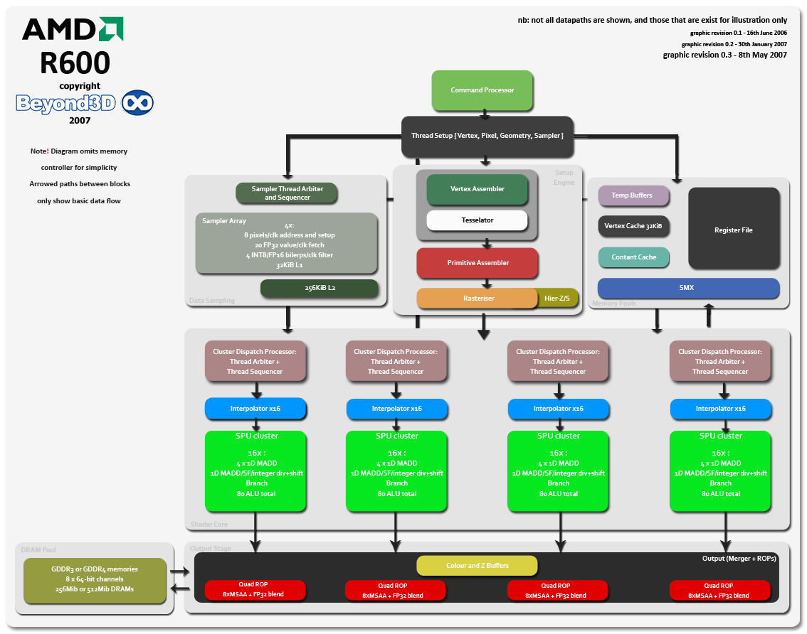
We use an image display overlay for image enlargement at Beyond3D (if your browser supports it), but it might be worth having the enlargement open in a new brower window or a new tab, so you can refer to it as the article goes by. The image represents a (fairly heavily in places) simplified overview of R600. Datapaths aren't complete by any means, but they serve to show the usual flow of data from the front of the chip to its back end when final pixels are output to the framebuffer and drawn on your screen. Hopefully all major processing blocks and on-chip memories are shown.
R600 is a unified, fully-threaded, self load-balancing shading architecture, that complies with and exceeds the specification for DirectX Shader Model 4.0. The major design goals of the chip are high ALU throughput and maximum latency hiding, achieved via the shader core, the threading model and distributed memory accesses via the chip's memory controller. A quick glance at the architecture, comparing it to their previous generation flagship most of all, shows that the emphasis is on the shader core and maximising available memory bandwidth for 3D rendering (and non-3D applications too).
The shader core features ALUs that are single precision and IEEE754 compliant in terms of rounding and precision for all math ops, with integer processing ability combined. Not all R600 SPUs are created equal, with a 5th more able ALU per SPU group that handles special function and some extra integer processing ops. R600, and the other GPUs in the same architecture family, also sports a programmable tesselation unit, very similar to the one found in the Xbox 360. While DirectX doesn't support it in any of its render stages, it's nonetheless programmable using that API with minimal extra code. The timeframe for that happening is unclear, though.
That's the basics of the processor, so we'll start to look at the details, starting with the front end of the chip where the action starts.
Command Processor, Thread Setup and Setup Engine
Command Process and Thread Setup

The command processor and thread setup are what get the chip doing useful work, accepting a command stream and data from the driver, which in turn is working on data provided to it by the graphics API asking the hardware to do something. The command processor in R600 is also responsible for validating hardware state asked for by the application, to make sure it's configured properly for any given set of ops needed to be executed. Previously the driver was entirely responsible for state checking, but D3D10 compliance mandates the hardware do at least some of the job to reduce CPU overhead when drawing. Combined with runtime overhead reduction in D3D10 as a whole and the simple task of asking the GPU to do some work consumes less host cycles than before.
The command processor is able to snoop the state of the processing units on the chip, so that it doesn't set state needlessly when it's already configured the right way, or when it simply doesn't need to be set because the state being asked for is invalid. State validation on R600 is also applied to D3D9 apps on Vista or XP/2000, so they see some benefit too, the driver not implementing old state management routines needlessly when there's logic on the chip to accelerate that. Alongside state validation and setting, the command stream is processed by thread setup logic, which determines thread type and batches ops and data to be passed further down the chip.
Setup Engine

We split off thread setup as coming before the Setup Engine, but we could just as easily have grouped it in there. It's responsible for getting thread ops and data into the right shapes and formats for the shader core to chew on, before passing down a thread batch for the dispatch hardware to execute. You'll see that part of the chip later in the article. When it comes to vertex processing, the setup hardware is responsible for arranging data in card memory for optimal access, so that vertex fetch isn't memory bound. It's also responsible for configuring and feeding the tesselator.
The tesselator is pretty much the same programmable unit in the Xenos processor in Xbox 360, which allows the developer to take a simple poly mesh and subdivide it based on a surface evaluation function. That function helps setup the maximum tesselation factor, how the subdivision rules should be applied to the mesh (to support different subdivision surfaces), and how recursion should work for tesselating geometry created by the tesselator. As part of setup it's in the pre-shading stage and outputs geometry and texture coordinates for the geometry assembler to work on. We could write an entire article on the tesselator, how it works, how you program it inside of D3D even though it's not part of the API. Indeed we will, so apologies the details are somewhat light in this piece.
Tesselation is free in the sense that generated geometry almost never hits board memory, but that can happen and there's a cap on subdivision, and you can also be limited by the rasteriser we imagine, given certain input geometry and the evaluation function. More on that in the dedicated tesselator piece. Rasterisation generates fragment tiles from geometry, for the shader core to chew on, working to what we think is the same 16x16 screen tile method as the previous generation of Radeon hardware.
As part of improvements to setup, R600 implements tweaked hierarchical-Z, tuned for very high pixel counts where performance is maintained even for 4Mpixel or higher displays, and also hierarchical stencil. The hier-Z/S buffers represent different coarse grained looks at the depth and/or stencil values in a tile, to determine whether to throw away geometry before rasterisation, pre-shading, to limit the number of pixels sent through the hardware. Of course, early-Z in the traditional sense (testing and rejecting every pixel individually) also occurs, but hier-Z helps reduces the number of tests that have to be done as more pixels can be rejected in one go, and it also saves bandwidth. Each stage in the buffer pyramid contains a different number of discrete values for Z/S, which the hardware checks to decide whether or not to throw the tile away or send it down.
The setup engine also performs attribute interpolation according to the presented slides, to setup those for shading, although we have that logic shown in the shader core in our diagram. With setup complete, the engine dispatches ready threads, which can be variable size in terms of objects, to the shader core for further processing. The hardware can fetch 16 vertices per clock out of card memory, setup one complete triangle per clock (for a peak rate of 742Mtris/sec on HD 2900 XT)
The threading model is arguably one of the most important facets of AMD's latest graphics architecture, so we'll spend good time talking about that.
Threading and Branching

What we call the cluster dispatch processor is what controls execution across the clusters (AMD call them SIMDs) in the shader core, and there's a similar processor for the sampler array. Those logic blocks are what control the threading model that R600 implements, to hide latency and take advantage of unit pipelining in order to maintain instruction and data throughput through the entire chip. We'll go through the shader core's processing first.
Input from the setup engine fills up a triplet of command queues, one for each thread type, containing the threads the dispatch hardware runs on the shader core. Each cluster contains a pair of arbiters that run a pair of object threads at a time, per cluster, allowing four clocks of execution before new threads are swapped on and run in place. Thread tracking for execution is controlled by a scoreboarding system that lets the hardware run threads out of order on the cluster, tracking dependencies and other parameters (likely the ops being run, and registers being written to and read from) to decide what gets executed next, in place of the currently running threads.
Threads undergoing arbitration also have granular priority, affecting the decision making for what's being run. The basic heuristics are designed to put shader threads waiting on sampler data to sleep, to cover latency and run shading ops unhindered while that's taking place, and it's what you'll find any heavily parallel, heavily threaded design doing in terms of its threading model. The sequencer pair (one per arbiter) inside the dispatch processor is there to keep track of where a thread is at in terms of its block of execution. Data from the sequencer can feed back into the arbiter to let it know when a thread is about to finish running, so that new threads can be prepared to take a finishing thread's place.
Like competing architectures, R600 will scale back the number of threads in flight at any given time when there's severe register pressure, so that there's no thread stalling because the register file would otherwise be full. Branch granularity is 64 pixels, and we measure it to be most performant using our branching test when working on 4x4 blocks of screen-aligned quads (so 8x8 pixels). Testing our branching shader using other tiling arrangements for the texture we're sampling in the shader shows that something like 32x2, or 16x4 (or 2x32, or 4x16) are slower.
Instruction blocks and constants are kept by the dispatch processor on chip inside dedicated, virtualised cache memories. They're there to maximum efficiency and let the hardware grab thread state as quickly as possible when executing. Any cache miss here will force the thread that needs the data to sleep, and another thread is swapped on in place and the needed data fetched into the cache so it's ready when it wakes. A cache miss here can also force a thread's priority to be reduced, effectively moving it down the command queue, so that it might not be woken up as the next thread behind the one that took its place when it missed.
In terms of threads in flight just for the shader core, the hardware maintains a usual count of thousands (which can cover tens of thousands of objects), depending of course on the resources they want to use. In terms of the sampling threads, the heuristics are simpler because there's no register pressure to account for, just the requirement that the right data is in the right cache at the right time, so that a refetch because of a cache miss doesn't occur and chip throughput is high, hiding the latency of the data fetch and any post-fetch filtering.
The threading model working well is also a function of the memory controller's ability to marshal data around the chip from the main pools, including the DRAM pool on the board, to the myriad clients that want to consume data, and store it. We move on to the shader core next.
Shader Core
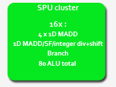
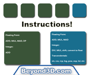
Ah, the processing guts of the beast. With four such clusters, R600 sports a full 320 separate processing ALUs dedicated to shading, with the units arranged as follows. Each cluster contains sixteen shader units, each containing five sub scalar ALUs that perform the actual shading ops. Each ALU can run a separate op per clock, R600 exploiting instruction-level parallelism via VLIW. Having the compiler/assembler do a bunch of the heavy lifting in terms of instruction order and packing, arguably reduces overall efficiency compared to something like G80's scalar architecture that can run full speed with dependent scalar ops. Not all the ALUs are equal, either, with the 5th in the group able to do a bit more than the other four, and independently of those too.
The VLIW design packs a possible 6 instructions per-clock, per-shader unit (5 shading plus 1 branch) into the complete instructions it issues to the shader units, and those possible instruction slots have to match the capabilities of the hardware underneath. Each of the first 4 sub ALUs is able to retire a finished single precision floating point MAD (or ADD or MUL) per clock, dot product (dp, and special cased by combining ALUs), and integer ADD. In terms of float precision, the ALUs are 1 ULP for MAD, and 1/2 ULP for MUL and ADD. The ALUs are split in terms of gates for float and int logic, too. There's no 32-bit mantissa in the ALU to support both, but only one datapath in and out of the sub-ALU, so no parallel processing there. Denorms are clamped to 0 for both D3D9 and D3D10, but the hardware supports inf. and NaN to IEE754 spec.
The fifth fatter unit (let's egotistically call it the RysUnit, since it shares my proportions compared to normal people, and I can be 'special' too) can't do dp ops, but is capable of integer division, multiply and bit shifting, and it also takes care of transcendental 'special' functions (like sin, cos, log, pow, exp, rcp, etc), at a rate of one retired instruction per clock (for most specials at least). It's also responsible for float<->integer conversion. Unlike the other units, this one is actually FP40 internally (32-bit mantissa, 8-bit exponent). This allows for single-cycle MUL/MAD operations on INT32 operands under D3D10, which G80 needs 4 cycles for. It's certainly an advantage of having a VLIW architecture and multiple kinds of units. If you didn't follow that, the following should help.
Each cluster runs thread pairs with the same type in any given cycle, but each of those four clusters can run a different thread type if it needs to. The front-end of the chip handles the thread load balancing across the core as mentioned, and there's nothing stopping all running threads in a given cycle being all pixel, all vertex, or even.....you guessed it: all geometry, although that might not be the case currently. More on that later.
For local memory access, the shader core can load/store from a huge register file that takes up more area on the die than the ALUs for the shader core that uses it. Accesses can happen in 'scalar' fashion, one 32-bit word at a time from the application writer's point of view, which along with the capability of co-issuing 5 completely random instructions (we tested using truly terrifying auto-generated shaders) makes ATI's claims of a superscalar architecture perfectly legit. Shading performance with more registers is also very good, indeed we've been able to measure that explicitly with shaders using variable numbers of registers, where there's no speed penalty for increasing them or using odd numbers. It's arguably one of the highlights of the design so far, and likely a significant contributor to R600's potential GPGPU performance as well.
Access to the register file is also cached, read and write, by an 8KiB multi-port cache. The cache lets the hardware virtualise the register file, effectively presenting any entry in the cache as any entry in the larger register file. It's unclear which miss/evict scheme they use, or if there's prefetching, but they'll want to maximise hits for the running threads of course.
It seems the hardware will also use it for streamout to memory, letting the shader core bypass the colour buffer and ROPs on the way out to board memory, and the chip will also use it for R2VB and overflow storage for GS amplification, making it quite the useful little piece of on-chip memory.
While going 5-way scalar has allowed AMD more flexibility in instruction scheduling compared to their previous hardware, that flexibility arguably makes your compiler harder to write, not easier. So as a driver writer you have more packing opportunities -- and I like to think of it almost like a game of Tetris when it comes to a GPU, but only with the thin blocks and with those being variable lengths, and you can sometimes break them up! -- those opportunities need handling in code and your corner cases get harder to find.
The end result here is a shader core with fairly monstrous peak floating point numbers, by virtue of the unit count in R600, its core clock and the register file of doom, but one where software will have a harder time driving it close to peak. That's not to say it's impossible, and indeed we've managed to write in-house shaders, short and long and with mixtures of channels, register counts and what have you, that run close to max theoretical thoughput. However it's a more difficult proposition for the driver tech team to take care of over the lifetime of the architecture, we argue, than their previous architecture.
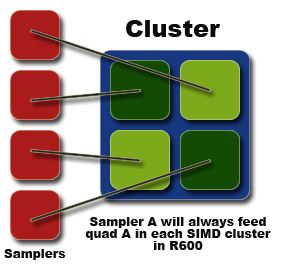
In terms of memory access from the sampler hardware, sampler units aren't tied to certain clusters as such, rather certain positions inside the cluster. If you visualise the 16 shader units in a cluster as being four quads of units, each of the four samplers in R600 is tied to one of those quads, and then across the whole shader core.
And it's the sampler hardware that we talk about next.
Data Sampling
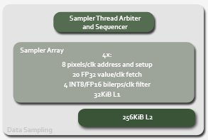
A significant upgrade in the shader core on any modern GPU, compared to a previous architecture generation, has to be matched elsewhere on the chip. Thus it's no honest surprise that R600 has improved sampling ability compared to R580 and R520, and you can argue it needs it given the hardware available on the competition's G80 GPU. R600 features a quartet of what they call texture units, but which we call samplers to reflect they can read and filter more than what you'd consider a traditional texture surface.
Each sampler unit can setup 8 addresses per clock, fetch 16 FP32 values for bilinear filtering, and 4 FP32 values for point sampling, all per clock, and then bilinearly filter at a rate of four INT8 or FP16 bilerps per cycle, from those fetched values. Don't believe what you read elsewhere about FP16 being half speed in R600, since it's simply not the case; 3- and 4-channel INT16 isn't full speed, NVIDIA getting a little confused. Our in-house sampler benchmark tool shows equivalent rates for INT8 and FP16 bilinear filtering with 1- to 4-channel fetches for small and large surfaces, which we'll show you later.
If you want to focus on unfiltered data fetches in your shader, the hardware can perform a Fetch4 fetch in place of the bilinear fetch, per clock. As mentioned on the previous page, each unit is tied to a certain sub 'quad' in a shader cluster, feeding the same one in each cluster in the shader core. 32-bit RGBE filtering is supported (as it has to be to comply with D3D10), for developers looking to use that shared exponent format for HDR rendering in their latest engines, and the chip can access very large textures up to 8Kx8K for any fetch or filtering ops.
All of the fetch and filtering capabilities are available to each thread type, making the samplers completely agnostic about what's using them. Each sampler unit is cached locally by a 32KiB local store, with a 256KiB shared L2 used to keep L1 misses around to reduce miss penalties from future requests striding across a collection of nearby addresses. The hardware will also use the vertex cache for accelerating unfiltered fetches. R600 also supports the same decompression formats out of cache that R580 did, for the likes of the DXT formats and ATI's 1- and 2-channel depth formats.
All filtering levels are available on all supported formats, including those in non-linear space, and with AMD supporting the same level selection and tap count for aniso that R580 did, image quality will remain subjectively high, but objectively less than the current competition. And despite whinging about its use in 3DMark, AMD now also support acceleration of depth stencil textures and PCF in R600, giving them a healthy per-clock boost in that benchmark if anyone cares about it.
The sampler unit count and their available performance means that while fetch and filter performance is increased over what's available in R580, it's one of the major areas where R600 is (sometimes heavily) deficient compared to NVIDIA G80 on a per clock basis, with the sampler units running at base clock like the rest of the chip. Like G80 and with the orthogonality in the sampler hardware, filtering power just becomes a product of available bilerps per clock, bandwidth permitting.
Of course the sampler hardware is fully threaded, with a dedicated arbiter and sequencer to manage execution, like the similar hardware that runs each R600 shader cluster, but with different heuristics to govern running threads because of the latency involved. Indeed the massively threaded nature of the sampler hardware is a means to hide latency, using the memory controller to make sure the shader core -- as a client of the sampler array via the MC -- is kept busy. Remember we said that the shader core would sleep threads while waiting on sampler data? The two schedulers work together to make sure that's the case, since a trip to a DRAM to open a page and get data, then feed it through the logic for filtering can be hundreds of clocks of wait time. You don't want to stall the shader core for that, at all.
The ROP hardware is next.
ROP

The ROP stage is likely going to be one of the most controversial parts of the R600 design for some time to come, given how AMD are making use of it in the shipping configurations. Basic abilities first, the ROP now supports 8x multisample AA using programmable sample grids, testing 4 positions per cycle with samples laid out over a 4-bit grid (16 discrete positions per pixel, X and Y, 256 total). It's able to test any supported surface format, including float surfaces. That means the hardware's basic multisample abilities match (and exceed by virtue of programability, you could argue) that of NVIDIA G80.
The blender is new, too, with one per ROP that's able to do any FP16 blend op in a single cycle, with FP32 half speed. Finished pixels come out of the ROP back-end at one per clock per ROP, the hardware making good use of available board bandwidth to sustain writes of floating point pixels into the framebuffer at that rate. It's a couple of GB/sec to sustain 60fps of FP16 pixel fill at 2560x1600, remember, never mind the memory bandwidth needed for every other op going on on the chip at the same time, to generate those frames!
The ROP will sustain a Z-only write rate of 2x compared to colour writes, even with AA enabled. Compression wise, AMD report that the depth and stencil compression logic for tiles is improved to the tune of 16:1, up from 8:1 in R5xx, and it scales with the AA level (so 128:1 at 8xMSAA, peak theoretically). The hardware will actively prefetch and cache tile compression data on-chip, to make sure it's available when decompressing for sample resolve. And that brings us on to probably the most controversial part of the chip: how does(n't) it do MSAA sample resolve.
Custom Filter AA
Custom Filter AA, or CFAA for short, is AMD implementing non-box filters that look outside the pixel being processed in order to calculate final colour and antialias the image. The sample resolve for that is performed on the shader core, data passed in so the programmable hardware can do the math, with the filter function defined by the driver. That means AMD can implement a pluggable user filter system if they want, but even if they don't they can update, add and remove filters from the driver at will whenever they see fit.
The big advantage is the ability to perform better filtering than the standard hardware resolve. However the disadvantages include possible implementation of bad filters, and speed issues because the driver now has to issue, and the hardware run, resolve calculation threads which chew up available shader core cycles. Ah, but there's still the regular hardware resolve if you want maximum speed and the regular quality just from sampling a single pixel, right? Well no, that's not always the case.
Even for the basic box filter resolves, where the hardware weights samples based on their proximity to the pixel centroid, R600 will perform the calculations to resolve the samples on the shader core, that is unless compression for the tile is at maximum, so you know the resolve would just return the same colour anyway, so there's no math involved to filter. Currently that points to the hardware resolve either being broken, at least under some conditions (when compression is less than maximum), or it being easier to maintain in code if you're doing other filters anyway, so you only have one path for that in the driver. We lean towards the former, rather than the latter, since the performance deficit for shader core resolve seems to be significant, even for the basic box filter cases. That can be improved in the driver, however, and the hardware helps here by likely being able to decompress sample locations for a pixel into the shader core at a high rate.
The current filters are wide and narrow tent filters, where samples from outside the pixel being processed are weighted linearly based on their distance from that pixel's centroid, with the linear function adjusted based on the wide or narrow choice. There's also an edge-detect mode that will analytically look for geometry edges intersecting the pixel based on an even wider search around it, and resolve with weight based on where they are and the direction of the edge itself (once determined). The cost for such a filter is pretty significant, and we'll examine that in the performance piece (it was only enabled in a usable driver bare days ago, at the time of writing).
Given the filter type, and the samples it takes from the pixel being processed and its surrounding neighbours, AMD still use somewhat usual nomenclature for naming the modes.
AMD R600 Custom Filter AA
|
|
Filter |
|
4x |
2x + Narrow Tent |
|
6x |
2x + Wide Tent or 4x + Narrow Tent |
|
8x |
4x + Wide Tent |
|
12x |
8x + Narrow Tent or 4x + Edge Detect |
|
16x |
4x + Wide Tent |
Because of sample positioning and the filter used, two of the modes can be achieved using different combinations of samples taken and filter used for resolve, with the number denoting total number of samples taken for the filter to work with. Because two of the modes don't have fixed quality (because there are two different ways to achieve the sample count, with different filters), you can't use the number part of a CFAA mode to determine if it's better quality than one with a higher or lower number, nor can you make any determination of speed.
It's also quite easy to imagine the tent filters, because of the way they look outside the target pixel, blurring the image because they too-heavily weight the contribution from samples in neighbouring pixels. At this stage in the real-time graphics game, we think it's advantageous to image quality as a whole if AA filter quality only ever gets better from the accepted norm, and never gets worse.
We're also not sure if the system will ever become fully custom in the sense that users will be able to write their own filters, and we're not sure if AMD will ever change or remove or add filters over time (indeed AMD aren't sure themselves at this point, since the functionality in the driver is actually quite new). We'll take a look at AA image quality quickly in a couple of pages time, and fully in the IQ article.
Display Output, Video
When it comes to display output, each member of the '6 family, including R600, had a display output pipe that's arguably at the pinnacle of what's available on any consumer add-in board (AIB) today. On all of the GPUs in the family, display output is twice dual-link DVI, one of the ports supporting AMD's HDMI solution, and with both links per port protected by an on-ASIC set of keys and a hardware encryption block. That means not only do you get the benefit of each DVI port supporting HDCP for each of its two links out of the on-chip TMDS transmitters, but that you also get HDMI output over one of the ports on every board.
The hardware supports up to 10 bits per colour component for final output, should you have a display that'll receive it on the other side, and the analogue DACs for each output run at 400MHz and are capable of driving multi megapixel resolutions on analogue display hardware, should you have something capable there, too.
The HDMI solution is a novel one, the board working with an active DVI-to-HDMI adapter to transmit audio out over the spare pins in a dual-link DVI port (the current revision of HDMI that R600 supports -- 1.2 -- is analagous to single-link DVI), audio provided by an on-chip HD Audio controller. Yes, the new Radeon's are also rudimentary HD Audio controllers, too, and all audio processing for that controller is currently done on the CPU. That makes it no less a solution to provide protected path audio out via encrypted HDMI, though, using one of the DVI ports on the board.
It remains to be seen if shipping products based on R600 will come with the active adapter that provides the conversion, or a HDMI cable too -- both of which would be significant value additions for any '6 family product -- but we're not expecting all R600-based products to have the adapter in the box, which is a shame. Hopefully it's not too hard to find for sale online if that's the case, and it shouldn't cost too much when it appears.
Video Processing
All '6-family products and the GPUs that drive them contain a new video decoder block, which AMD worked with Tensilica to build, called UVD, or Unified Video Decoder (we're convinced it was called Universal Video Decoder at some point, but that's an aside). The UVD is designed to offload the entire decode process for H.264, H.263 and VC-1 motion video, at the maximum bitrates defined by the DVD, Blu-Ray and HD-DVD controlling groups, so that every SKU of this new generation of Radeon could perform (almost) full CPU offload acceleration for video playback for all three current optical disc formats.
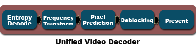
The five major stages of the UVD are shown above, with the entropy decode supporting full sped CABAC and CAVLC for H.264, and VC-1's entropy encode scheme, entirely in silicon. Compressed video data is fed in to the unit at the front end of the block, and then that's passed out for post processing by other hardware solutions on-chip, which differ depending on the GPU in the family.
R600 does all of its post processing for motion video on the shader core, implementing the filters needed entirely in shader programs that they can update and tweak as the driver matures. However the current driver for R600 gets a score of 128 in the Silicon Optix HQV benchmark for SD DVD, showing that things are already pretty mature, at least as far as SD video goes.
RV610 and RV630 have an evolution of AMD's Avivo technology for post processing, where it's done in a slightly programmable block which the driver can set state for before the post processing takes place. We'll take a look at video quality in a separate article.
Architecture Performance Analysis
While we look at game performance in another article to come soon, we've taken a good look at the base architecture performance, especially in terms of the shader core and filtering hardware, for this architecture analysis.
Shader Core Performance
Given the way the shader core works, each shader unit processing a single object per clock but having 5 independent ALUs available to do so, our existing shaders for testing available maximum throughput needed to be rewritten. We ran old and new shaders through two new test apps, one running the shaders through D3D9, one through D3D10, to check API-level performance differences (if any). The shaders aren't like any you'd find in a shipping game title or production app, but are explicitly designed to test the hardware's peak shader throughput.
The old codes contained streams of dependant instructions, mostly to defeat optimisations, which obviously trips R600 up when the operands are single component, running at approximately 1/5th peak ALU throughput. All shaders are run as pixel shaders, which is something we'll mix up in future versions of the tool, to test load balancing and multi-thread type throughputs.

So the basic performance tenets of the shader core hold up, with instruction throughput effectively the same via each API, and the compiler struggling a little with our independent MAD shader in terms of seeing peak (some 236.8Ginst/sec at 740MHz). The dependent shader tests show that what an architecture like G80 will eat up, an architecture like R600 will struggle with, the hardware unable to schedule free instructions on the remaining ALUs. Of course these are best and worst cases for scalar throughput; take a look at a shipping game shader and you'll find channel widths varying, massively variant instruction mixes and other opportunities for hardware like R600 to schedule intelligently.
While we've not had time to check everything out, we also note that transcendentals all seem to run at 1 per clock, barring RCP which seems to run at half speed (at least in our simple shader). We also note that float-to-int conversion is one clock per scalar channel being converted (as is going back in the other direction from int to float), and that the hardware will do dp4 in one clock if all four thin ALUs are free (and the same for dp3 and dp2 of course). We've got a more extensive set of integer benchmark tests on the way, that'll we'll run back to back on G80 and R600. Theoretically, maximum integer throughput should be very high on R600 for ADD, when the hardware can schedule it.
The thing to take away from base architecture performance is that you can push max theoretical throughput through the shader core for any given instruction in isolation. We haven't tested every instruction, but we're confident that's the case. Of course the architecture means that the compiler has to get things right there, but that's been the case for all of their previous programmable architectures, so we're sure they're able to handle the most common optimisation cases for the chip, and it'll likely get better over time as they take a look at different mixes.
We were able to test filtering and ROP throughput too, so that's next.
Architecture Performance Analysis
Filtering Performance
Our filtering throughput tester takes a look at a bunch of formats, varying channels for some, and outputs in terms of texture ops per second. We take a look at the bilinear and point sampling results for INT8, INT16 and FP16 in this article, concentrating on 1- and 4-channel results. In our performance analysis piece we'll take a look at RGBE (9:9:9:5) and FP10 as well, and also flesh out the 2- and 3-channel results, since there's also some interesting data there. We'll also add in 8800 GTS, and X1950 XTX. We focus on INT8 and FP16 here as common surface formats, and INT16 because it's seen a recent high profile use in a D3D10 application.
We sample from a 4x4 texture to get max performance, sampling all texels from the texture cache as much as possible. Compared to G80, R600 has one quarter the INT8 bilerp rate available, and one half the FP16 bilerp rate, per clock. Remember Radeon HD 2900 XT runs the sampler hardware at 740MHz, and we use GeForce 8800 GTX as the initial folly, since it's the highest clocked G80 we have access to at the time of writing.
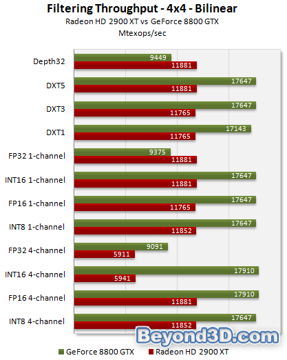
R600 is full speed for INT8 and FP16 bilinear filtering (including with 4-channel surfaces), when bandwidth permits (we're just reading out of cache here for all 16 texels), as claimed. For other uncompressed formats, the hardware will scale back to half speed for 4-channel versus 1, although with G80 scaling differently it enjoys higher 1-channel FP32 filtering performance because of its clock (they run at the same rate, clocks normalised).
So even though 4-channel FP16 is free on R600, INT16 doesn't enjoy the same performance because the precision available to the sampler hardware isn't (there's not enough mantissa available), and it drops back to half speed as noted. G80's sampler hardware has sufficient precision to maintain the rate. In terms of D32F filtering (Depth32 on the graph), R600 runs full speed, and the format is useful for pretty much every shadowing implementation out there, bar VSM.
Point sampling shows much the same picture for the formats we test:

ROP throughput
We've done a little work with the ROPs, too, to check out throughput. We test colour, colour+Z and Z-only fill, full screen.
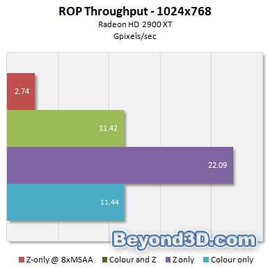
The sustained double Z rate claimed is in evidence, with colour writes turned off, and you can see Z-only fill drop off as expected with 8xMSAA enabled (it's ¼ with 4xMSAA, not shown). You'll see how ROP throughput translates to real-world performance in the IQ and Performance parts of our fuller R600 analysis.
Image Quality
Anisotropic Filtering Level Selection
R600 implements almost the same level selection algorithm as R580 (and the other chips in the same architecture family) in high-quality mode, which means the default selection is almost angle invariant, but not to the degree that competing hardware is. We show the 16xAF pattern here before taking a closer look at full-frame image quality in the IQ piece.

Note the peaks at 45° angle multiples. If you want to take a look at output for other hardware before we take a closer look, you can reference our G80 image quality analysis.
Antialiasing Grids and Quality
We show the base MSAA sample positions for 4x and 8x MSAA, using Colourless's tester. They're the subpixel sample patterns used for all AA modes, including CFAA ones, with the filter just reading samples from neighbouring pixels with the same positions.
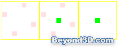
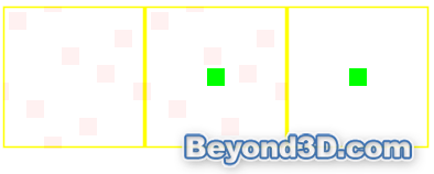
Note that you get 4x4 and 8x8 EER, AMD ensuring that the default sample locations all have discrete planar values for X and Y. We note that temporal AA doesn't seem to be enabled, at least in the Vista driver, since Colourless's tester doesn't show them moving if you advance frame-by-frame, as you normally would. We use nonatainment's AA tester to grab edge quality in each of the modes.
0x

2x Box - 2 samples

2x Narrow Tent - 4 samples

2x Wide Tent - 6 samples

4x Box - 4 samples

4x Narrow Tent - 6 samples

4x Wide Tent - 8 samples

8x Box - 8 samples

8x Narrow Tent - 12 samples

8x Wide Tent - 16 samples

4x Edge Detect - 12 samples

8x Edge Detect - 24 samples

The general rule is that edge quality increases with sample count, for each mode, which is what you'd expect. For example, in this test 2x Wide arguably has better edge quality than 4x Box, and given the sample count it makes sense in terms of the raw numbers of samples being taken and used for final pixel resolve. However, our high-contrast examples here don't really show the whole story, since the new CFAA filters affect more than just edge quality. Before we take a look at that a bit closer, we should point out that the edge detect modes look comparatively excellent, too. Compare the 24-sample edge detect mode to NVIDIA's 16xQ CSAA mode, for an example. Both have very good edge quality, but note the pixels near the 'nose' of the shape being AA'd, on the left, in both.
Image Quality
In-game AA quality
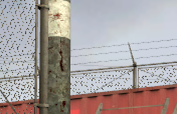
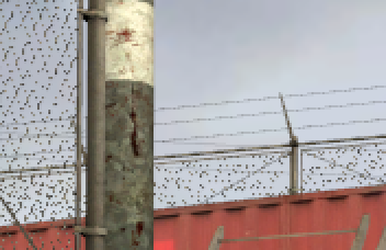
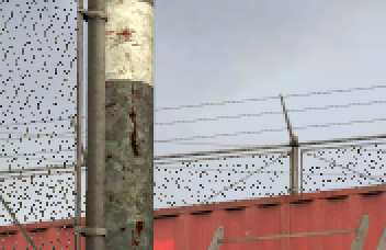
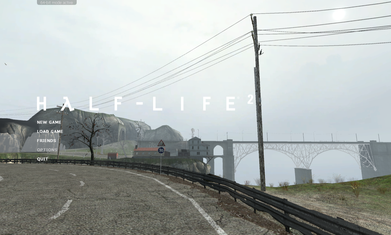
We use a cropped and 200% zoomed (when you click on the cropped version) section of a static screenshot from Half-Life 2, which features thin geometry, alpha textures and a decent textured portion so you can see the AA at work.
2x Box - 2 samples

2x Narrow Tent - 4 samples

2x Wide Tent - 6 samples

4x Box - 4 samples
4x Narrow Tent - 6 samples
4x Wide Tent - 8 samples

8x Box - 8 samples
8x Narrow Tent - 12 samples

8x Wide Tent - 16 samples

4x Edge Detect - 12 samples

8x Edge Detect - 24 samples
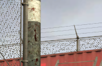
Again, pure edge quality goes up with the number of samples taken, regardless of filter. Thin geometry on screen gets a nice boost from the tent filtered modes, we note. Look closer at the vertical pole and the container in the background and you'll see (sometimes subtle, sometimes not) blurring of the image and a reduction in overall image quality, when using the tent filtered modes. Edge detect is a different story though, with much less blurring (although analytically there'll likely still be some, because of the filter) and excellent edge quality. The 8x box filtered mode is subjectively as good as NVIDIA's 8x (8xQ) mode. Sample locations are different, but the aggregate quality using a sum of all histories approach and because of the EER of the mode means that they'll be equivalent overall.
We could present a boatload of examples that show the blurring property of the tent filters, even the narrow one, but we're sure you get the idea and we'll show you, and take a closer look at how the filters work mathematically, in the image quality piece.
Add adaptive AA into the mix with the edge detect mode, though, and you get pretty awesome quality.
8x Edge Detect + Quality Adaptive AA


For reasonably high contrast edges like those power lines against the sky in our test frame, the edge quality is arguably as good as it had ever been on consumer hardware, and you can see the AA on the alpha textured fence via the adaptive mode. It's worth noting that when OpenGL or D3D ask for AA with R600, they'll only ever get the box filtered mode. CFAA is a user choice, and it's not clear if AMD will work to get applications able to activate CFAA in any sane way.

Note that there's no choice for the edge detect mode, and that currently you need to turn it on and off either by editing the Windows Registry and forcing a reload of the display driver somehow (resolution change is one way), or by using a small tool AMD developed to force it on and off. It'll be rolled into a public driver soon though, we're sure. We also wonder if NVIDIA will ponder an edge detect mode for their hardware, and we think it's likely they'll at least experiment in that area.
Architecture Summary
Well well, graphics fans, it's finally here! Years in the making for AMD, via the hands of 300 or so engineers, hundreds of millions of dollars in expenditure, and unfathomable engineering experience from the contributing design teams at AMD, R600 finally officially breaks cover. We've been thinking about the architecture and GPU implementations for nearly a year now in a serious fashion, piecing together the first batches of information sieved from yon GPU information stream. As graphics enthusiasts, it's been a great experience to finally get our hands on it and put it through the mill of an arch analysis, after all those brain cycles spent thinking about it before samples were plugged in and drivers installed.
So what do we think, after our initial fumblings with the shader core, texture filter hardware and ROPs? Well arguably the most interesting bits and pieces the GPU and boards that hold them provide, we've not been able to look at either for time reasons, resource reasons, or they simply fall outside this article's remit! That's not to say things like the UVD, HDMI implementation and the tesselator overshadow the rest of the chip and architecture, but they're significant possible selling points that'll have to await our judgement a little while longer.
What remains is a pretty slick engineering effort from the guys and guys at AMD's Graphics Products Group, via its birth at the former ATI. What you have is evolution rather than revolution in the shader core, AMD taking the last steps to fully superscalar with independent 5-way ALU blocks and a register file with seemingly no real-world penalty for scalar access. That's backed up by sampler hardware with new abilities and formats supported to chew on, with good throughput for common multi-channel formats. Both the threaded sampler and shader blocks are fed and watered by an evolution of their ring-bus memory controller. We've sadly not been able to go into too much detail on the MC, but mad props to AMD for building a 1024-bit bi-directional bus internally, fed by a 16-piece DRAM setup on the 512-bit external bus.
Who said the main IHVs would never go to 512? AMD have built that controller in the same area as the old one (whoa, although that's helped by the process change), too. Using stacked pads and an increase in wire density, affording them the use of slower memory (which is more efficient due to clock delays when running at higher speeds), R600 in HD 2900 XT form gets to sucking over 100GB/sec peak theoretical bandwidth from the memories. That's worth a tip of an engineer's hat any day of the week.
Then we come to the ROP hardware, designed for high performance AA with high precision surface formats, at high resolution, with an increase in the basic MSAA ability to 8x. It's here that we see the lustre start to peel away slightly in terms of IQ and performance, with no fast hardware resolve for tiles that aren't fully compressed, and a first line of custom filters that can have a propensity to blur more than not. Edge detect is honestly sweet, but the CFAA package feels like something tacked on recently to paper over the cracks, rather than something forward-looking (we'll end up at the point of fully-programmable MSAA one day in all GPUs) to pair with speedy hardware resolve and the usual base filters. AMD didn't move the game on in terms of absolute image quality when texture filtering, either. They're no longer leaders in the field of IQ any more, overtaken by NVIDIA's GeForce 8-series hardware.
Coming back to the front of the chip, the setup stage is where we find the tesselator. Not part of a formal DirectX spec until next time with DX11, it exists outside of the main 3D graphics API of our time, and we hope the ability to program it reliably comes sooner rather than later since it's a key part of the architecture and didn't cost AMD much area. We'll have a good look at the tesselator pretty soon, working with AMD to delve deep into what the unit's capable of.
With a harder-to-compile-for shader core (although one with monstrous floating point peak figures), less per-clock sampler ability for almost all formats and channel widths, and a potential performance bottleneck with the current ROP setup, R600 has heavy competition in HD 2900 XT form. AMD pitch the SKU not at (or higher than) the GeForce 8800 GTX as many would have hoped, but at the $399 (and that's being generous at the time of writing) GeForce 8800 GTS 640MiB. And that wasn't on purpose, we reckon. If you asked ATI a year ago what they were aiming for with R600, the answer was a simple domination over NVIDIA at the high end, as always.
While we take it slow with our analysis -- and it's one where we've yet to heavily visit real world game scenarios, DX10 and GPGPU performance, video acceleration performance and quality, and the cooler side facets like the HDMI solution -- the Beyond3D crystal ball doesn't predict the domination that ATI will have done a year or more ago. Early word from colleagues at HEXUS, The Tech Report and Hardware.fr in that respect is one of mixed early performance that's 8800 GTS-esque or thereabouts overall, but also sometimes less than Radeon X1950 XTX in places. Our own early figures there show promise for AMD's new graphics baby, but not everywhere.
It's been a long time since that's been something anyone's been able to say about a leading ATI, now AMD, graphics part. We'll know a fuller story as we move on to looking at IQ and performance a bit closer, with satellite pieces to take in the UVD and HDMI solution and the tesselator to come as well. However after our look at the base architecture, we know that R600 has to work hard for its high-quality, high-resolution frames per second, but we also know AMD are going to work hard to make sure it gets there. We really look forward to the continued analysis of a sweet and sour graphics architecture in the face of stiff competition, and we'll have image quality for you in a day or two to keep things rolling. RV610 and RV630 details will follow later today.

 浙公网安备 33010602011771号