wallys/QCN9074 802.11ax 4x4 2.4GHz wifi6 QCN9074 11ax 4x4 MU-MIMO 2.4G M.2
QCN9074 802.11ax 4x4 2.4GHz wifi6
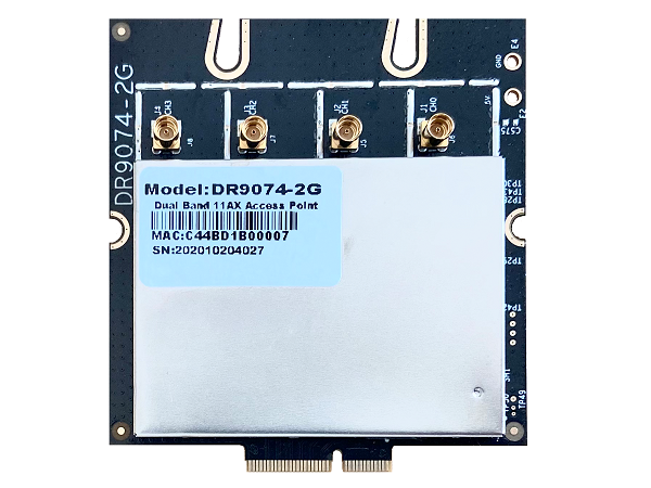
DR9074-2.4G(PN01.1)
MT7915/MT7975/IPQ6000/IPQ6018/IPQ6010/IPQ4019/IPQ4029/ipq4018/IPQ4028/IPQ8072/IPQ8072A/IPQ8074/IPQ8074A/IPQ9074/QCN9074/QCN9072/QCN9024/IPQ5018/AR9223/QCA9880/QCA9882 /AR9582/AR9531/AR9344
BY:Wallys Communications (Suzhou ) Co., LTD
EMAIL:sales3@wallystech.com
Wallys Communications (Suzhou ) Co., LTD(http://www.wallystech.com) is a professional supplier of wireless communication products and has a complete industrial chain in China. Our biggest advantage is our independent research and development ability, which can support you in the later period.
DR9074-2.4G(PN01.1)
https://www.wallystech.com/Network_Card/DR9074-2.4G-PN01.1-Wifi-6-Qualcomm-QCN9074-Single-Band-2.4-GHz-4T4R-M.2-E-Key-Interface-802.11ax.html
Features
■ Qualcomm Atheros QCN9074
■ 2.4GHz, max 23dBm per chain, up to 1147Mbps
■ Single Band 2.4GHz 4x4 WiFi 6 (802.11ax
■ 4 spatial streams (4SS)
■ M.2 E Key Interface
■ PCI Express 3.0 Interface
|
Absolute Maximum Rating |
|
Parameter |
Rating |
Unit |
|
Operating Temperature Range |
-20 to 70 |
ºC |
|
Storage Temperature Range |
-40 to 90 |
ºC |
|
Operating Humidity Range |
5 to +95 (non-condensing) |
% |
|
Storage Humidity Range |
0 to +90 (non-condensing) |
% |
| Hardware Specifications |
|
Symbol |
Parameter |
|
Chipset |
Qualcomm Atheros QCN9074 |
|
WLAN Host Interface |
PCI Express 3.0 Interface |
|
System Memory |
2Mbit serial I²C bus EEPROM |
|
Standard Operating Voltage |
5V |
|
Operating Systems |
QSDK |
|
Host Interface |
M.2 E Key |
|
Antenna Cable / Port |
4 x MMCX Connectors,4T4R |
|
Frequency Range |
2.412GHz-2.472GHz |
|
Data Rates for WALN |
2.4GHz, max 23dBm per chain, up to 4949Mbps |
|
Channel Spectrum Widths for WLAN |
Support 20/40MHz at 2.4GHz |
|
Modulation Techniques |
OFDMA: BPSK, QPSK, DBPSK, DQPSK,16-QAM, 64-QAM, 256-QAM,1024-QAM |
|
Temperature Range |
Operating: -20°C to 70°C, Storage: -40°C to 90°C |
|
Humidity |
Operating: 5% to 95% (non-condensing), Storage: Max. 90% (non-condensing) |
|
Certification |
TBD |
|
Power Consumption |
TBD |
|
Reference Design |
PN01.1 |
|
Dimensions (WxHxD) |
57mm x 63mm x 6mm |
| M.2 Pin Definitions |
| Pin No. | Name | Pin No. | Name |
| 1 |
GND |
2 |
VDD3P3_PCIE |
| 3 |
|
4 |
VDD3P3_PCIE |
| 5 |
|
6 |
PCIE_LED0 |
| 7 |
GND |
8 |
GPIO46_WCI2_UART_TXD_PCIE |
| 9 |
TP19 |
10 |
GPIO47_WCI2_UART_RXD_PCIE |
| 11 |
|
12 |
|
| 13 |
|
14 |
|
| 15 |
VDD_XPA_PCIE |
16 |
PCIE_LED1 |
| 17 |
VDD_XPA_PCIE |
18 |
GND |
| 19 |
VDD_XPA_PCIE |
20 |
|
| 21 |
VDD_XPA_PCIE |
22 |
|
| 23 |
VDD_XPA_PCIE |
|
|
|
|
|
|
|
| 33 |
GND |
32 |
|
| 35 |
PCIE0_RX0_P |
34 |
|
| 37 |
PCIE0_RX0_N |
36 |
|
| 39 |
GND |
38 |
MOD_BT_STS_2 |
| 41 |
PCIE0_TX0_P |
40 |
MOD_WL_ACT_2 |
| 43 |
PCIE0_TX0_N |
42 |
PINE_BT_ACT_2 |
| 45 |
GND |
44 |
MOD_BT_STS |
| 47 |
PCIE0_REFCLK_P |
46 |
MOD_WL_ACT |
| 49 |
PCIE0_REFCLK_N |
48 |
PINE_BT_ACT |
| 51 |
GND |
50 |
|
| 53 |
PCIE0_CLKREQ_3P3_N |
52 |
PCIE0_PERST_3P3 |
| 55 |
PCIE0_WAKE_3P3_N |
54 |
|
| 57 |
GND |
56 |
|
| 59 |
PCIE0_RX1_P |
58 |
|
| 61 |
PCIE0_RX1_N |
60 |
|
| 63 |
GND |
62 |
|
| 65 |
PCIE0_TX1_P |
64 |
|
| 67 |
PCIE0_TX1_N |
66 |
|
| 69 |
GND |
68 |
|
| 71 |
|
70 |
|
| 73 |
|
72 |
VDD3P3_PCIE |
| 75 |
GND |
74 |
VDD3P3_PCIE
|

 浙公网安备 33010602011771号