The CircuitCalculator.com Blog a blog with live web calculators Home About Policies Contact PCB
关键词:
PCB,Layout,电流,导线宽度。
This Javascript web calculator calculates the trace width for printed circuit boards based on a curve fit to IPC-2221 (formerly IPC-D-275). Also see thevia calculator.
New features:
- Results update as you type
- Several choices of units
- Units and other settings are saved between sessions
- Blog format allows user comments
Inputs:
| Current | Amps | |
| Thickness |
Optional Inputs:
| Temperature Rise | Deg | |
| Ambient Temperature | Deg | |
| Trace Length |
Results for Internal Layers:
| Required Trace Width | ||
| Resistance | Ohms | |
| Voltage Drop | Volts | |
| Power Loss | Watts |
Results for External Layers in Air:
| Required Trace Width | ||
| Resistance | Ohms | |
| Voltage Drop | Volts | |
| Power Loss | Watts |
Notes:
The trace width is calculated as follows:
First, the Area is calculated:
Area[mils^2] = (Current[Amps]/(k*(Temp_Rise[deg. C])^b))^(1/c)
Then, the Width is calculated:
Width[mils] = Area[mils^2]/(Thickness[oz]*1.378[mils/oz])
For IPC-2221 internal layers: k = 0.024, b = 0.44, c = 0.725
For IPC-2221 external layers: k = 0.048, b = 0.44, c = 0.725
where k, b, and c are constants resulting from curve fitting to the IPC-2221 curves
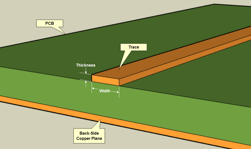
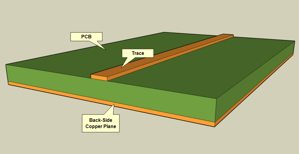
For geometry diagrams, click on the pictures below.
For frequently asked questions, see the comments.

 浙公网安备 33010602011771号