ADC分类及参数
ADC分类
- 直接转换模拟数字转换器(Direct-conversion ADC),或称Flash模拟数字转换器(Flash ADC)
- 循续渐近式模拟数字转换器(Successive approximation ADC)
- 跃升-比较模拟数字转换器(Ramp-compare ADC)
- 威尔金森模拟数字转换器(Wilkinson ADC
- 集成模拟数字转换器(Integrating ADC)
- Delta编码模拟数字转换器(Delta-encoded ADC)
- 管道模拟数字转换器(Pipeline ADC)
- Sigma-Delta模拟数字转换器(Sigma-delta ADC)
- 时间交织模拟数字转换器(Time-interleaved ADC)
- 带有即时FM段的模拟数字转换器
- 时间延伸模拟数字转换器(Time stretch analog-to-digital converter, TS-ADC
1、闪速型
2、逐次逼近型
3、Sigma-Delta型
1. 闪速ADC
闪速ADC是转换速率最快的一类ADC。闪速ADC在每个电压阶跃中使用一个比较器和一组电阻。
2. 逐次逼近ADC
逐次逼近转换器采用一个比较器和计数逻辑器件完成转换。
转换的第一步是检验输入是否高于参考电压的一半,如果高于,将输出的最高有效位(MSB)置为1。
然后输入值减去输出参考电压的一半,再检验得到的结果是否大于参考电压的1/4,依此类推直至所有的输出位均置“1”或清零。
逐次逼近ADC所需的时钟周期与执行转换所需的输出位数相同。
3. Sigma-delta ADC
Sigma-delta ADC采用1位DAC、滤波和附加采样来实现非常精确的转换,转换精度取决于参考输入和输入时钟频率。
Sigma -delta转换器的主要优势在于其较高的分辨率。
闪速和逐次逼近ADC采用并联电阻或串联电阻,这些方法的问题在于电阻的精确度将直接影响转换结果的精确度。
尽管新式ADC采用非常精确的激光微调电阻网络,但在电阻并联中仍然不甚精确。
sigma-delta转换器中不存在电阻并联,但通过若干次采样可得到收敛的结果。
Sigma-delta转换器的主要劣势在于其转换速率。
由于该转换器的工作机理是对输入进行附加采样,因此转换需要耗费更多的时钟周期。
在给定的时钟速率条件下,Sigma-delta转换器的速率低于其它类型的转换器;
或从另一角度而言,对于给定的转换速率,Sigma-delta转换器需要更高的时钟频率。
Sigma-delta转换器的另一劣势在于将占空(duty cycle)信息转换为数字输出字的数字滤波器的结构很复杂,
但Sigma-delta转换器因其具有在IC裸片上添加数字滤波器或DSP功能而日益得到广泛应用。
Atmel AVR127: Understanding ADC Parameters
This application note is about the basic concepts of analog-to-digital converter (ADC) and the parameters that determine the performance of an ADC.
These ADC parameters are of good importance since they determine the accuracy of the ADC’s output.
The parameters can be broadly classified into static performance parameters and dynamic performance parameters.
Static performance parameters are those parameters that are not related to ADC’s input signal.
These parameters are measured and analyzed for all types of ADCs
(ADCs integrated within the microcontroller or standalone ADCs whose operating frequency are usually higher).
Instead, dynamic performance parameters are related to ADC’s input signal and their effects are significant with higher frequencies.
Major static parameters include gain error, offset error, full scale error and linearity errors
whereas some important dynamic parameters include signal-to-noise ratio (SNR), total harmonic distortion (THD),
signal to noise and distortion (SINAD) and effective number of bits (ENOB).
Basic Concepts
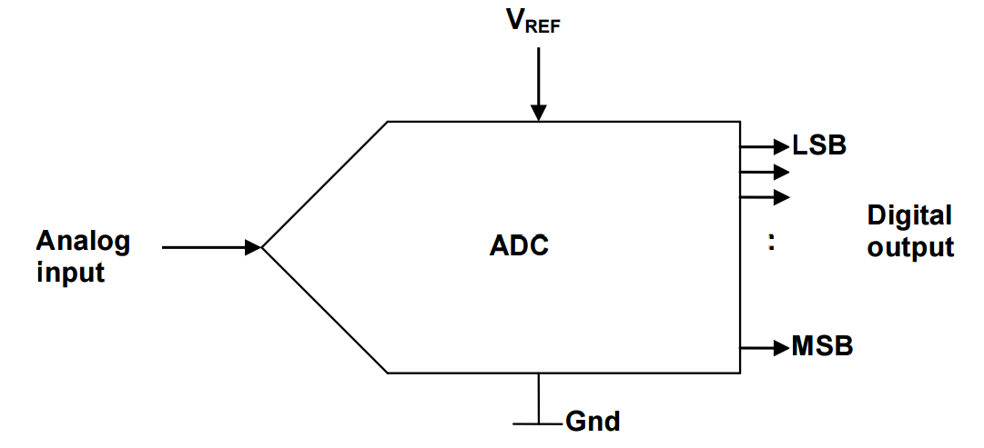
An ADC is an electronic system or a module that has analog input, reference voltage input and digital outputs.
The ADC convert the analog input signal to a digital output value that represents the size of the analog input comparing to the reference voltage.
It basically samples the input analog voltage and produces an output digital code for each sample taken.
Figure 1-1. Basic diagram of ADC
To get a better picture about the ADC concepts, let us first look into some basic ADC terms used.
1.1 Input Voltage Range
The input voltage range of an ADC is determined by the reference voltage (VREF) applied to the ADC.
A reference voltage can be either internal voltage or external voltage by applying a voltage on an external pin of the microcontroller.
Generally reference voltage can be selected by configuring the corresponding register’s bit field of the microcontroller.
ADC will saturate with a analog voltage higher than the reference voltage,
so the designer must make sure that the analog input voltage does not exceed the reference voltage.
The input voltage range is also called as conversion range.
If ADC runs in signed mode (the mode produces signed output codes), it allows negative analog input voltages.
In such cases the analog input range is from –VREF to +VREF.
An ADC which accepts both positive and negative input voltages is called as bipolar ADC
whereas an ADC that accepts only positive input voltage is called as unipolar ADC.
1.2 Resolution
The entire input voltage range (from 0V to VREF) is divided into a number of sub-ranges.
Each sub range is assigned a single output digital code.
A sub range is also called LSB (least significant bits) and the number of sub ranges is usually in powers of two.
The total number of sub ranges is called the resolution of the ADC.
For an example, an ADC with eight LSBs has the resolution of three bits (2^3 = 8).
If an ADC’s resolution is three bits then it also means that the code width of the output is three bits.
1.3 Quantization
The LSB is determined if input analog voltage lies in the lowest sub-range of the input voltage range.
For example, consider an ADC with VREF as 2V and resolution as three bits.
Now the 2V is divided into eight sub-ranges, so the LSB voltage is within 250mV.
Now an input voltage of 0V as well as 250mV is assigned to the same output digital code 000.
This process is called as quantization.
1.4 Conversion Mode
A conversion mode determines how the ADC processes the input and performs the conversion operation.
A standard ADC has basically two types of conversion modes.
1. Single ended conversion mode.
2. Differential conversion mode.
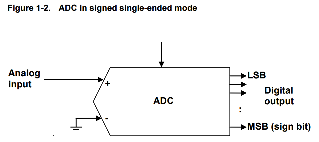
1.4.1 Single Ended Conversion Mode
In single ended conversion, only one analog input is taken and the ADC sampling and conversion is done on that input.
In single ended conversion ADC can be configured to operate in unsigned or signed mode.
The analog is connected to ADC has non-inverting(+) input and inverting(-) input
which should be differently connected under signed or unsigned mode.
For example in signed mode of operation, the single-ended input may be given to the non-inverting input of the ADC
and the inverting input of the ADC is grounded.
This is depicted in Figure 1-2. In this case the reference voltage is from – VREF to + VREF,
which means it allows negative input voltages.
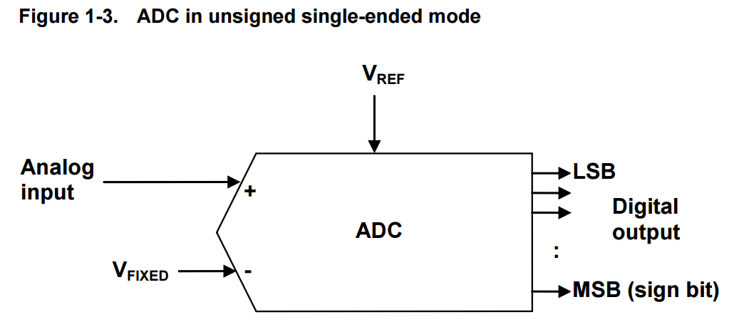
In unsigned single-ended mode, the single-ended input is given to the non-inverting input of the ADC
as before and the inverting input of the ADC is supplied with some fixed voltage value VFIXED
which is usually half of the reference voltage minus a fixed offset) as shown in Figure 1-3.
In this case the input voltage range is from 0V to VREF, which means it does not allows negative input voltages.
1.4.2 Differential Conversion
In differential conversion mode, two analog inputs are taken and applied to the inverting and non-inverting inputs of the ADC,
either directly or after doing some amplification by selecting some programmable amplification stages (gain amplifier stage).
Differential conversions are usually operated in signed mode, where the MSB of the output code acts as the sign bit.
Also the reference voltage is from - VREF to +VREF for signed mode. This is shown in the Figure 1-4

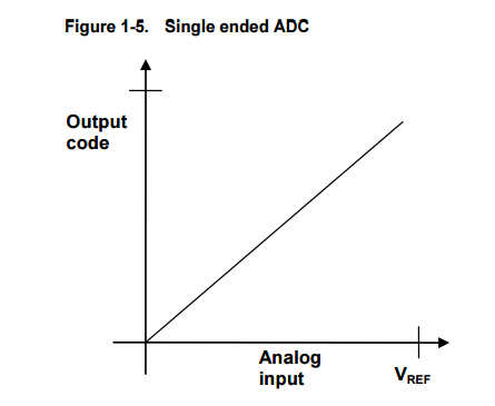
1.5 Ideal ADC
An ideal ADC is just a theoretical concept, and cannot be implemented in real life.
It has infinite resolution, where every possible analog input value gives a unique digital output
from the ADC within the specified conversion range.
An ideal ADC can be described mathematically by a linear transfer function, as shown in Figure 1-5 and Figure 1-6.

1.6 Perfect ADC
To define a perfect ADC, the concept of quantization must be used.
Due to the digital nature of an ADC, continuous output values are not possible.
The perfect ADC performs the quantization process during conversion.
This results in a staircase transfer function where each step represents one LSB.
If the reference voltage is 2V, say, and the ADC resolution is three bits,
then the step width becomes 250mV (1LSB).
The input analog voltage range from 0V to 250mV will be assigned the digital output code 000
and the input analog voltage range from 251mV to 500mV will be assigned the digital code 001 and so on.
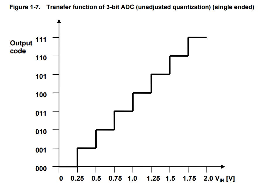
This is depicted in Figure 1-7 which shows the transfer function of a perfect 3-bit ADC operating in single ended mode.
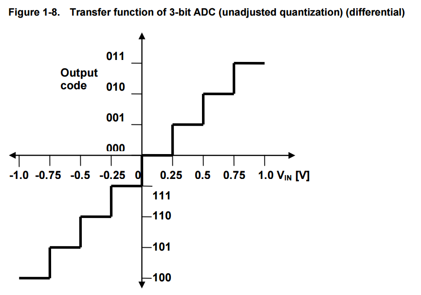
Figure 1-8, given below, shows the transfer function of a perfect 3-bit ADC operating in differential mode.
NOTE The reference voltage is from -1V to +1V in this case and the MSB acts as sign bit.
From the Figure 1-7, it is obvious that an input voltage of 0V produces an output code 000.
At the same time, an input voltage of 250mV also produces the same output code 000.
This explains the quantization error due to the process of quantization.
As the input voltage rises from 0V, the quantization error also rises from 0LSB
and reaches a maximum quantization error of 1LSB at 250mV.
Again the quantization error increases from 0 to 1LSB as the input rises from 250mV to 500mV.
This maximum quantization error of 1LSB can be reduced to ±0.5LSB by shifting the transfer function towards left through 0.5LSB.
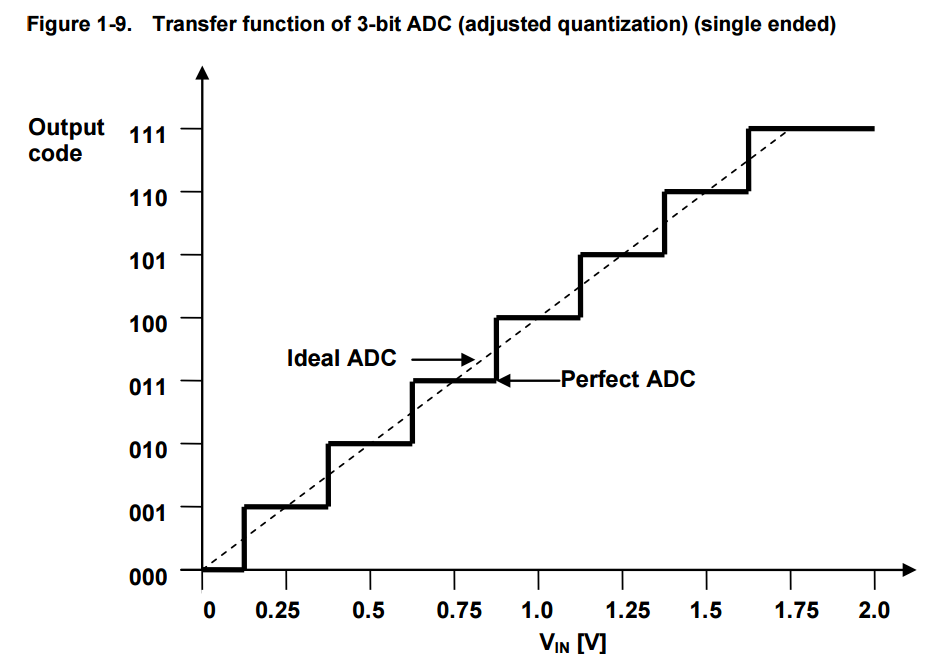
Figure 1-9 depicts the quantization adjusted perfect transfer function together with the ideal transfer function.
As seen on the figure, the perfect ADC equals the ideal ADC on the exact midpoint of every step.
This means that the perfect ADC essentially rounds input values to the nearest output step value.
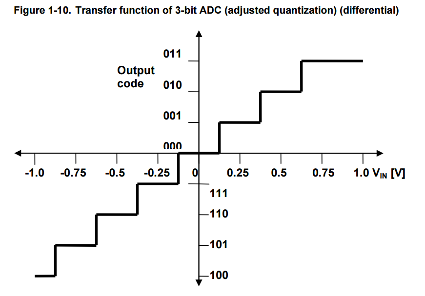
Similarly Figure 1-10 is for differential ADC.
Quantization error is the only error when perfect ADC is considered.
But in case of real ADC, there are several other errors other than quantization error as explained below.
1.7 Offset Error
The offset error is defined as the deviation of the actual ADC’s transfer function
from the perfect ADC’s transfer function at the point of zero to the transition measured in the LSB bit.
When the transition from output value 0 to 1 does not occur at an input value of 0.5LSB,
then we say that there is an offset error.
With positive offset errors, the output value is larger than 0 when the input voltage is less than 0.5LSB from below.
With negative offset errors, the input value is larger than 0.5LSB when the first output value transition occurs.
In other words, if the actual transfer function lies below the ideal line, there is a negative offset and vice versa.
Positive and negative offsets are shown in Figure 1-11 and Figure 1-12 respectively measured with double ended arrows.
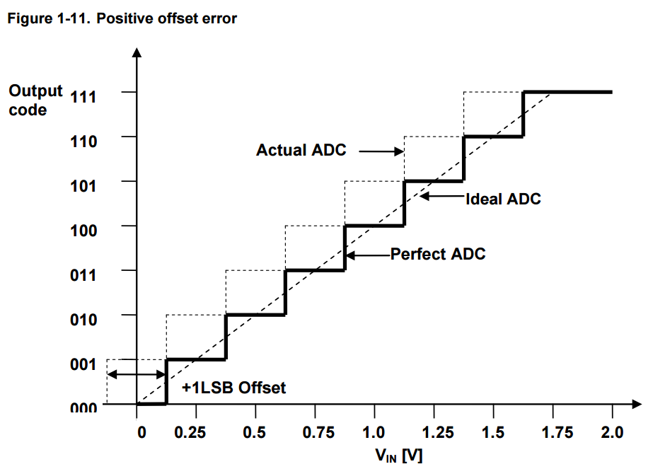
In Figure 1-11, the first transition occurs at 0.5LSB and the transition is from 1 to 2.
But 1 to 2 transitions should occur at 1.5LSB for perfect case.
So the difference (Perfect – Real = 1.5LSB – 0.5LSB = +1LSB) is the offset error.
Similarly in the Figure 1-12, the first transition occurs at 2LSB and the transition is from 0 to 1.
But 0 to 1 transition should occur at 0.5LSB for perfect case.
So the difference (Perfect – Real = 0.5LSB – 2LSB = -1.5LSB) is the offset error.
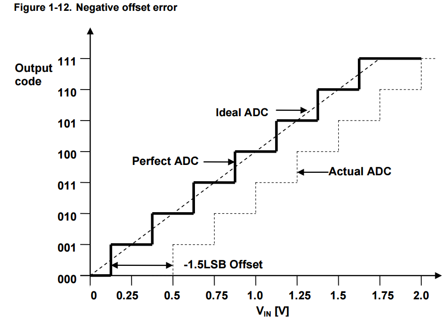
It should be noted that offset errors limit the available range for the ADC.
A large positive offset error causes the output value to saturate at maximum before the input voltage reaches maximum.
A large negative offset error gives output value 0 for the smallest input voltages.
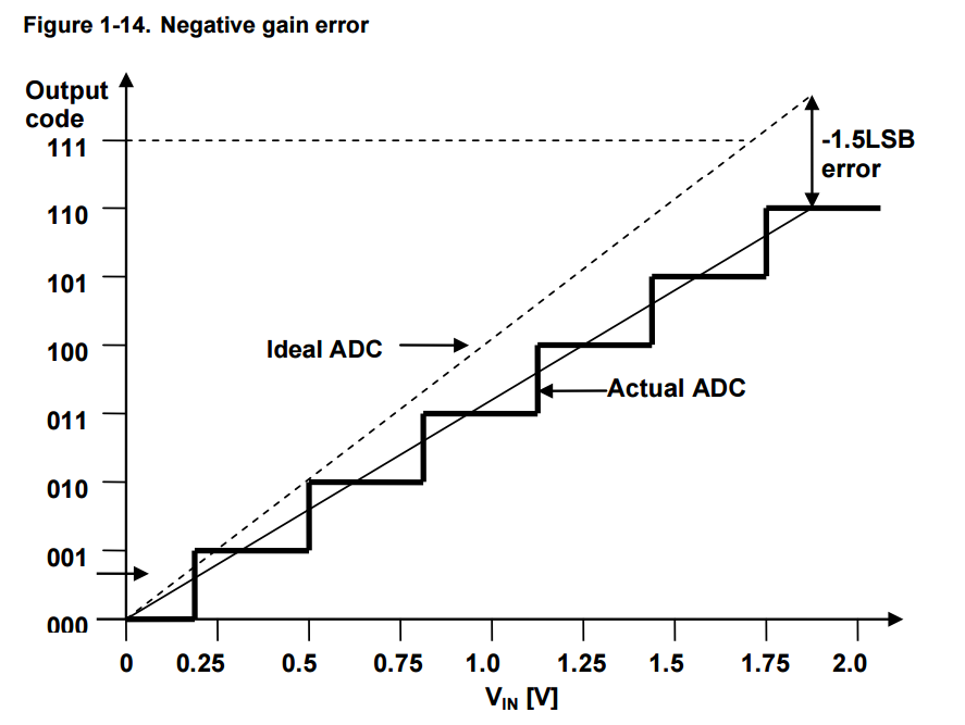
1.8 Gain Error
The gain error is defined as the deviation of the last step’s midpoint of the actual ADC from the last step’s midpoint of the ideal ADC,
after compensated for offset error.
After compensating for offset errors, applying an input voltage of 0 always give an output value of 0.
However, gain errors cause the actual transfer function slope to deviate from the ideal slope.
This gain error can be measured and compensated for by scaling the output values.
The example of a 3-bit ADC transfer function with gain errors is shown in Figure 1-13and Figure 1-14.
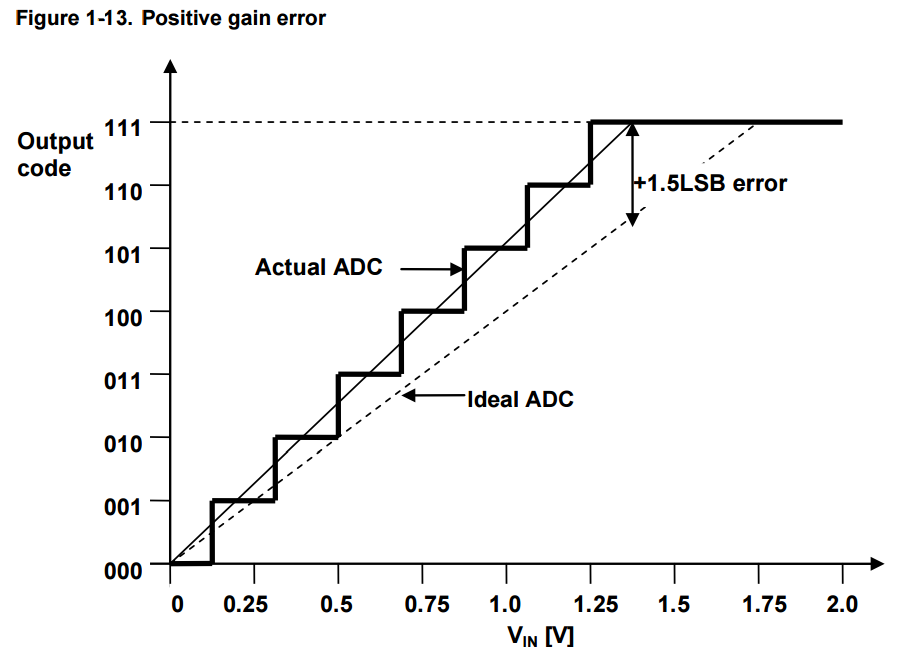
If the transfer function of the actual ADC occurs above the ideal straight line, then it produces positive gain error and vice versa.
The gain error is calculated as LSBs from a vertical straight line drawn between the midpoint of the last step of the actual transfer curve and the ideal straight line.
In Figure 1-13, the output value saturates before the input voltage reaches its maximum.
The vertical arrow shows the midpoint of the last output step.
In Figure 1-14, the output value has only reached six when the input voltage is at its maximum.
This results in a negative deviation for the actual transfer function.
1.9 Full Scale Error
Full scale error is the deviation of the last transition (full scale transition) of the actual ADC
from the last transition of the perfect ADC, measured in LSB or volts.
Full scale error is due to both gain and offset errors.
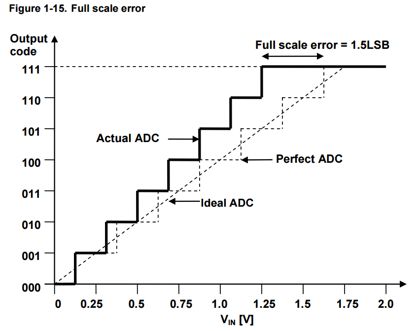
In Figure 1-15, the deviation of the last transitions between the actual and ideal ADC is 1.5LSB.
1.10 Non-linearity
The gain and offset errors of the ADC can be measured and compensated using some calibration procedures. When offset and gain errors are compensated for, the actual transfer function should now be equal to the transfer function of perfect ADC. However, non-linearity in the ADC may cause the actual curve to deviate slightly from the perfect curve, even if the two curves are equal around 0 and at the point where the gain error was measured. There are two major types of non-linearity that degrade the performance of ADC. They are differential non-linearity (DNL) and integral non-linearity (INL).
1.10.1 Differential non-linearity (DNL)
Differential non-linearity (DNL) is defined as the maximum and minimum difference in the step width between actual transfer function and the perfect transfer function. Non-linearity produces quantization steps with varying widths, some narrower and some wider.
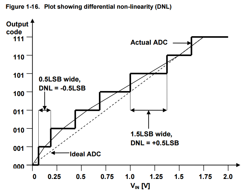
For the case of ideal ADC, the step width should be 1LSB.
But an ADC with DNL shows step widths which are not exactly 1LSB.
In Figure 1-16, in a maximum case the width of the step with output value 101 is 1.5LSB which should be 1LSB.
So the DNL in this case would be +0.5LSB. Whereas in a minimum case, the width of the step with output value 001 is only 0.5LSB which is 0.5LSB less than the expected width. So the DNL now would be ±0.5LSB.
1.10.2 Missing code
There are some special cases wherein the actual transfer function of the ADC would look as in the Figure 1-17.
In the example below, the first code transition (from 000 to 001) is caused by an input change of 250mV. This is exactly as it should be. The second transition, from 001 to 010, has an input change that is 1.25LSB, so is too large by 0.25LSB. The input change for the third transition is exactly the right size. The digital output remains constant when the input voltage changes from 1000mV to 1500mV and the code 100 can never appear at the output. It is missing. the highter the resolution of the ADC is, of the less severity the missing code is. An ADC with DNL error less than ±1LSB guarantees no missing code.

1.10.3 Integral non-linearity (INL)
Integral non-linearity (INL) is defined as the maximum vertical difference between the actual and the ideal curve.
It indicates the amount of deviation of the actual curve from the ideal transfer curve.

INL can be interpreted as a sum of DNLs. For example several consecutive negative DNLs raise the actual curve above the ideal curve as shown in Figure 1-16 and the INL in this case would be positive. Negative INLs indicate that the actual curve is below the ideal curve. This means that the distribution of the DNLs determines the integral linearity of the ADC. The INL can be measured by connecting the midpoints of all output steps of actual ADC and finding the maximum deviation from the ideal curve in terms of LSBs. From the Figure 1-18, we can note that the maximum INL is +0.75LSB.
1.11 Absolute error
Absolute error or absolute accuracy is the total uncompensated error and includes quantization error, offset error, gain error and non-linearity. So in a perfect case, the absolute error is 0.5LSB which is due to the quantization error. Gain and offset errors are more significant contributors of absolute error. The absolute error represents a reduction in the ADC range. So users should therefore consider keep some margins against the minimum and maximum input values to avoid the absolute error impact.
1.12 Signal to noise ratio (SNR)
SNR is defined as the ratio of the output signal voltage level to the output noise level. It is usually represented in decibels (dBs) and calculated with the following formula.
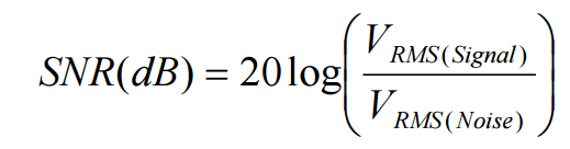
For example if the output signal amplitude is 1V(RMS) and the output noise amplitude is 1mV(RMS),
then the SNR value would be 60dB. To achieve better performance, the SNR value should be higher.
The above mentioned formula is a general definition for SNR. The SNR value of an ideal ADC is given by:
SNR (dB) = 6.02N+1.76(dB)
where N is the resolution (no. of bits) of the ADC.
For example an ideal 10-bit ADC will have an SNR of approximately 62dB.
1.13 Total harmonic distortion (THD)
Whenever an input signal of a particular frequency passes through a non-linear device, additional content is added at the harmonics of the original frequency. For example, assume an input signal having frequency f. Then the harmonic frequencies are 2f, 3f, 4f, etc. So non-linearity in the converter will produce harmonics that were not present in the original signal. These harmonic frequencies usually distort the output which degrades the performance of the system. This effect can be measured using the term called total harmonic distortion (THD). THD is defined as the ratio of the sum of powers of the harmonic frequency components to the power of the fundamental/original frequency component. In terms of RMS voltage, the THD is given by,
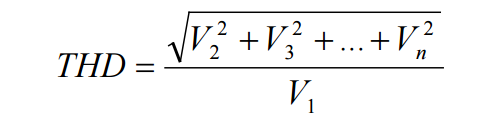
The THD should have minimum value for less distortion. As the input signal amplitude increases, the distortion also increases. The THD value also increases with the increase in the frequency.
1.14 Signal to noise and distortion (SINAD)
Signal to noise and distortion (SINAD) is a combination of SNR and THD parameters. It is defined as the ratio of the RMS value of the signal amplitude to the RMS value of all other spectral components, including harmonics, but excluding DC. For representing the overall dynamic performance of an ADC, SINAD is a good choice since it includes both the noise and distortion components. SINAD can be calculated with SNR and THD as given below.
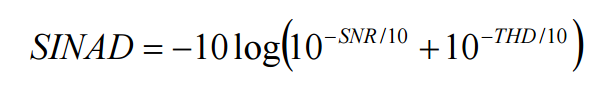
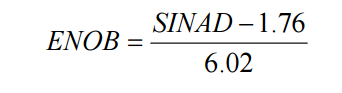
1.15 ENOB
Effective number of bits (ENOB) is the number of bits with which the ADC behaves like a perfect ADC.
It is another way of representing the signal to noise ratio and distortion (SINAD) and is derived from the formula specified in Section 2.11 as given below:
1.16 ADC timings
Basically an ADC takes some time for startup, sampling and holding and for conversion.
Out of these, the startup time is more concerned with ADCs of high end microcontrollers that operate at higher frequencies.
1.16.1 Startup time
Startup time contains the minimum time (in clock cycles) needed to guarantee the best converted value
after the ADC has been enabled either for the first time or after a wake up from some of the sleep modes.
1.16.2 Sample and hold time
Usually after giving a trigger to an ADC to start a conversion, it take some time (in clock cycles) to charge the internal capacitor to a stable value so that the conversion result is accurate. This time is called as sample time. This time must be considered carefully especially when multiple channels are used during conversion. In such case there is a minimum time (in clock cycles) needed to guarantee the best converted value between two ADC channel switching. After the sampling time, the number of clock cycles it takes to convert the charge or the voltage across the internal sampling capacitor into corresponding digital code is called the hold time.
1.16.3 Settling time
When using multiple channels, there may be cases in which each channel may have different gain and offset configurations. Switching between these channels requires some amount of time, before beginning the sample and hold phase, in order to have good results. Especially care should be taken when switching between differential channels. Once a differential channel is selected, the ADC should wait for some amount of time for some of the analog circuits (for example the automatic offset cancellation circuitry) to stabilize to the new value. This time is called as settling time. So ADC conversion should not be started before this time. Doing so will produce an erroneous output. The same settling time should be observed for the first differential conversion after changing the ADC reference.
1.16.4 Conversion time
Conversion time is the combination of the sampling time and the hold time, usually represented in number of clock cycles. The conversion time is the main parameter in deciding the speed of the ADC. Also the startup time, sample and hold time and the settling time are all software configurable in ADC’s of some high end microcontrollers.
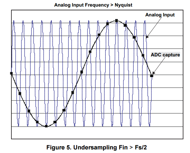
1.17 Sampling rate, throughput rate and bandwidth
Sampling rate is defined as the number of samples in one second.
Bandwidth represents the maximum frequency of the input analog signal that can be given to the ADC.
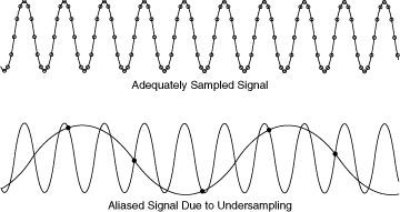
Sampling rate and bandwidth follow Nyquist sampling theorem.
为了不失真地恢复模拟信号,采样频率应该不小于模拟信号频谱中最高频率的2倍。
Fs ≥ Fn = 2 Fh
采样率越高,稍后恢复出的波形就越接近原信号,但是对系统的要求就更高,转换电路必须具有更快的转换速度。
采样是将一个信号(即时间或空间上的连续函数)转换成一个数值序列(即时间或空间上的离散函数)。采样定理指出,
如果信号是带限的,并且采样频率大于信号带宽的2倍,那么,原来的连续信号可以从采样样本中完全重建出来。
从信号处理的角度来看,此采样定理描述了两个过程:
其一是采样,这一过程将连续时间信号转换为离散时间信号;
其二是信号的重建,这一过程离散信号还原成连续信号。
从采样定理中,我们可以得出结论:
如果已知信号的最高频率fH,采样定理给出了保证完全重建信号的最低采样频率。
这一最低采样频率称为临界频率或奈奎斯特频率,通常表示为fN
相反,如果已知采样频率,采样定理给出了保证完全重建信号所允许的最高信号频率。
以上两种情况都说明,被采样的信号必须是带限的,即信号中高于某一给定值的频率成分必须是零,
或至少非常接近于零,这样在重建信号中这些频率成分的影响可忽略不计。
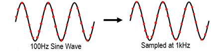
在第一种情况下,被采样信号的频率成分已知,比如声音信号,由人类发出的声音信号中,
频率超过5 kHz的成分通常非常小,因此以10 kHz的频率来采样这样的音频信号就足够了。
在第二种情况下,我们得假设信号中频率高于采样频率一半的频率成分可忽略不计。
这通常是用一个低通滤波器来实现的。
According to this theorem, the sampling rate should be at least twice the bandwidth of the input signal.
Consider the case of single ended conversion where one conversion takes 13 ADC clock cycles.
Assuming the ADC clock frequency to be 1MHz, then approximately 77k samples will be converted in one second.
That means the sampling rate is 77k.
So according to Nyquist theorem, the maximum frequency of the analog input signal is limited to 38.5kHz
which represents the bandwidth of the ADC in single ended mode.
Taking the same case above, if 1MHz is the maximum clock frequency
that can be applied to an ADC which takes at least 13 ADC clock cycles for converting one sample,
then 77k samples per second is said to be the maximum throughput rate of the ADC.
When using differential mode, the bandwidth is also limited to the frequency of the internal differential amplifier.
So before giving the analog input to the ADC, any frequency components above the mentioned bandwidth
should be filtered using external filter to avoid any non-linearity


1.18 Impedances and capacitances of ADC
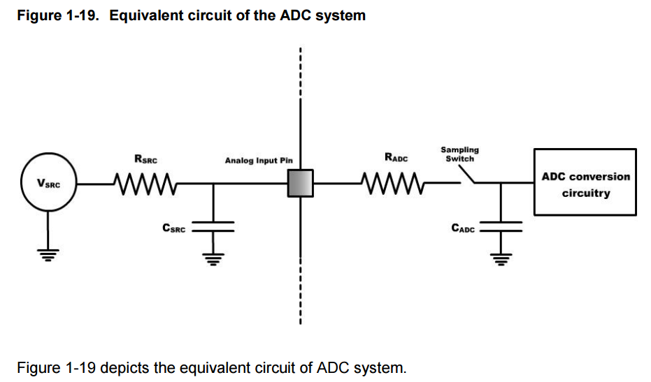
Inside the ADC, the sample and hold circuit of the ADC contains a resistance-capacitance (RADC & CADC) pair in a low pass filter arrangement.
The CADC is also called as sampling capacitor. Whenever an ADC start conversion signal is issued, the sampling switch between the RADC – CADC pair is closed so that the analog input voltage charges the sampling capacitor through the resistance RADC. T
he input impedance of the ADC is the combination of RADC and the impedance of the capacitor.
As the sampling capacitor gets charged to the input voltage, the current through RADC reduces and ends up with a minimum value when voltage across the sampling capacitor equals the input voltage. So the minimum input impedance of the ADC equals RADC.
In the source side, the ideal source voltage is subject to some resistance called the source resistance (RSRC) and some capacitance called source capacitance (CSRC) present in the source module. Because of the presence of RSRC, the current entering the sample and hold circuit reduces.
So this reduction in current increases the time to charge the sampling capacitance thereby reducing the speed of the ADC. Also the presence of CSRC makes the source to first charge it completely before charging the sampling capacitor.
This reduces the accuracy of the ADC since the sampling capacitor may not be completely charged.
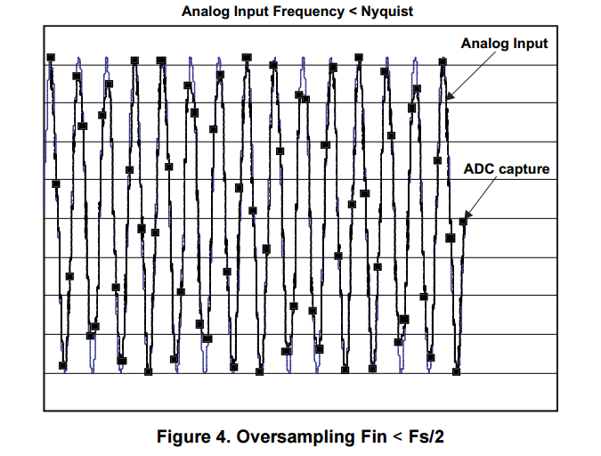
1.19 Oversampling
Oversampling is a process of sampling the analog input signal at a sampling rate significantly higher than the Nyquist sampling rate.
The main advantages of oversampling are:
1. It avoids the aliasing problem, since the sampling rate is higher compared to the Nyquist sampling rate.
2. It provides a way of increasing the resolution of the ADC. For example, to implement a 14-bit converter,
it is enough to have a 10-bit converter which can run at 256 times the target sampling rate.
Averaging a group of 256 consecutive 10-bit samples adds four bits to the resolution of the average,
producing a single sample with 14-bit resolution.
3. The number of samples required to get additional n bits is = 22n .
4. It improves the SNR of the ADC.
Understanding analog to digital converter specifications
Confused by analog-to-digital converter specifications? Here's a primer to help you decipher them and make the right decisions for your project.
Although manufacturers use common terms to describe analog-to-digital converters (ADCs), the way ADC makers specify the performance of ADCs in data sheets can be confusing, especially for a newcomers. But to select the correct ADC for an application, it's essential to understand the specifications. This guide will help engineers to better understand the specifications commonly posted in manufacturers' data sheets that describe the performance of successive approximation register (SAR) ADCs.
ABCs of ADCs
ADCs convert an analog signal input to a digital output code. ADC measurements deviate from the ideal due to variations in the manufacturing process common to all integrated circuits (ICs) and through various sources of inaccuracy in the analog-to-digital conversion process. The ADC performance specifications will quantify the errors that are caused by the ADC itself.
ADC performance specifications are generally categorized in two ways: DC accuracy and dynamic performance. Most applications use ADCs to measure a relatively static, DC-like signal (for example, a temperature sensor or strain-gauge voltage) or a dynamic signal (such as processing of a voice signal or tone detection). The application determines which specifications the designer will consider the most important.
For example, a DTMF decoder samples a telephone signal to determine which button is depressed on a touchtone keypad. Here, the concern is the measurement of a signal's power (at a given set of frequencies) among other tones and noise generated by ADC measurement errors. In this design, the engineer will be most concerned with dynamic performance specifications such as signal-to-noise ratio and harmonic distortion. In another example, a system may measure a sensor output to determine the temperature of a fluid. In this case, the DC accuracy of a measurement is prevalent so the offset, gain, and nonlinearities will be most important.
DC accuracy
Many signals remain relatively static, such as those from temperature sensors or pressure transducers. In such applications, the measured voltage is related to some physical measurement, and the absolute accuracy of the voltage measurement is important. The ADC specifications that describe this type of accuracy are offset error, full-scale error, differential nonlinearity (DNL), and integral nonlinearity (INL). These four specifications build a complete description of an ADC's absolute accuracy.
Although not a specification, one of the fundamental errors in ADC measurement is a result of the data-conversion process itself: quantization error. This error cannot be avoided in ADC measurements. DC accuracy, and resulting absolute error are determined by four specs—offset, full-scale/gain error, INL, and DNL. Quantization error is an artifact of representing an analog signal with a digital number (in other words, an artifact of analog-to-digital conversion). Maximum quantization error is determined by the resolution of the measurement (resolution of the ADC, or measurement if signal is oversampled). Further, quantization error will appear as noise, referred to as quantization noise in the dynamic analysis. For example, quantization error will appear as the noise floor in an FFT plot of a measured signal input to an ADC, which I'll discuss later in the dynamic performance section).
The ideal transfer function
The transfer function of an ADC is a plot of the voltage input to the ADC versus the code's output by the ADC. Such a plot is not continuous but is a plot of 2N codes, where N is the ADC's resolution in bits. If you were to connect the codes by lines (usually at code-transition boundaries), the ideal transfer function would plot a straight line. A line drawn through the points at each code boundary would begin at the origin of the plot, and the slope of the plot for each supplied ADC would be the same as shown in Figure 1.
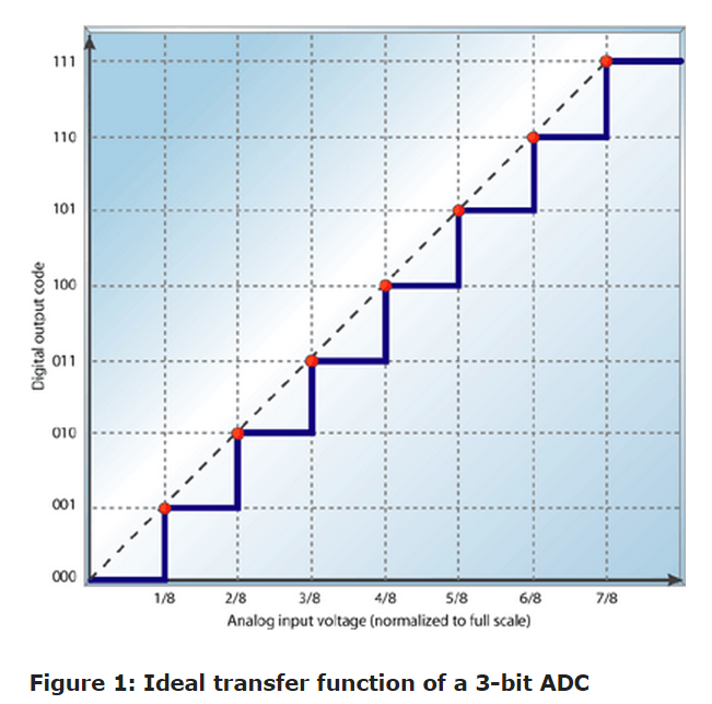
Figure 1 depicts an ideal transfer function for a 3-bit ADC with reference points at code transition boundaries. The output code will be its lowest (000) at less than 1/8 of the full-scale (the size of this ADC's code width). Also, note that the ADC reaches its full-scale output code (111) at 7/8 of full scale, not at the full-scale value. Thus, the transition to the maximum digital output does not occur at full-scale input voltage. The transition occurs at one code width—or least significant bit (LSB)—less than full-scale input voltage (in other words, voltage reference voltage).
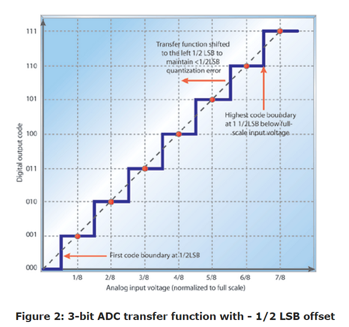
The transfer function can be implemented with an offset of - 1/2 LSB, as shown in Figure 2. This shift of the transfer function to the left shifts the quantization error from a range of (- 1 to 0 LSB) to (- 1/2 to +1/2 LSB). Although this offset is intentional, it's often included in a data sheet as part of offset error (see section on offset error).
Limitations in the materials used in fabrication mean that real-world ADCs won't have this perfect transfer function. It's these deviations from the perfect transfer function that define the DC accuracy and are characterized by the specifications in a data sheet.
The DC performance specifications described have accompanying figures that depict two transfer function segments: the ideal transfer function (solid, blue lines) and a transfer function that deviates from the ideal with the applicable error described (dashed, yellow line). This is done to better illustrate the meaning of the performance specifications.
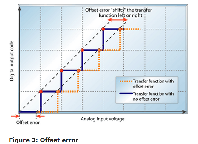
Offset error, full-scale error
The ideal transfer function line will intersect the origin of the plot. The first code boundary will occur at 1 LSB as shown in Figure 1. You can observe offset error as a shifting of the entire transfer function left or right along the input voltage axis, as shown in Figure 3.
An error of - 1/2 LSB is intentionally introduced into some ADCs but is still included in the specification in the data sheet. Thus, the offset-error specification posted in the data sheet includes 1/2 LSB of offset by design. This is done to shift the potential quantization error in a measurement from 0 to 1 LSB to - 1/2 to +1/2 LSB. In this way, the magnitude of quantization error is intended to be < 1/2 LSB, as Figure 4 illustrates.
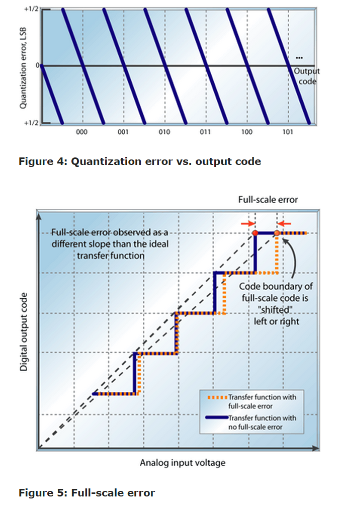
Figure 5: Full-scale error
Full-scale error is the difference between the ideal code transition to the highest output code and the actual transition to the output code when the offset error is zero. This is observed as a change in slope of the transfer function line as shown in Figure 5. A similar specification, gain error, also describes the nonideal slope of the transfer function as well as what the highest code transition would be without the offset error. Full-scale error accounts for both gain and offset deviation from the ideal transfer function. Both full-scale and gain errors are commonly used by ADC manufacturers.
Nonlinearity
Ideally, each code width (LSB) on an ADC's transfer function should be uniform in size. For example, all codes in Figure 2 should represent exactly 1/8th of the ADC's full-scale voltage reference. The difference in code widths from one code to the next is differential nonlinearity (DNL). The code width (or LSB) of an ADC is shown in Equation 1.
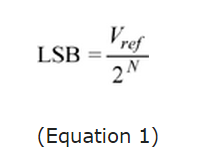
The voltage difference between each code transition should be equal to one LSB, as defined in Equation 1.
Deviation of each code from an LSB is measured as DNL.
This can be observed as uneven spacing of the code "steps" or transition boundaries on the ADC's transfer-function plot.
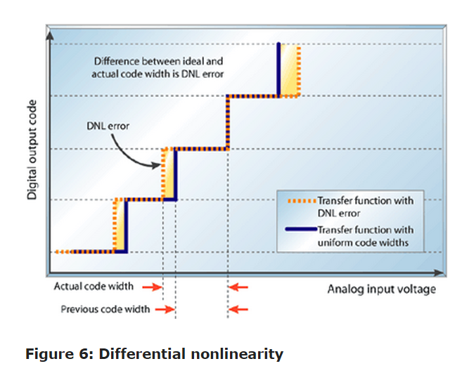
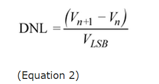
In Figure 6, a selected digital output code width is shown as larger than the previous code's step size. This difference is DNL error. DNL is calculated as shown in Equation 2.
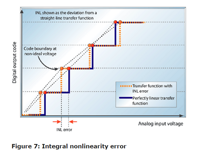
The integral nonlinearity (INL) is the deviation of an ADC's transfer function from a straight line. This line is often a best-fit line among the points in the plot but can also be a line that connects the highest and lowest data points, or endpoints. INL is determined by measuring the voltage at which all code transitions occur and comparing them to the ideal. The difference between the ideal voltage levels at which code transitions occur and the actual voltage is the INL error, expressed in LSBs. INL error at any given point in an ADC's transfer function is the accumulation of all DNL errors of all previous (or lower) ADC codes, hence it's called integralnonlinearity. This is observed as the deviation from a straight-line transfer function, as shown in Figure 7.
 .
.
Because nonlinearity in measurement will cause distortion, INL will also affect the dynamic performance of an ADC.
Absolute error
The absolute error is the total DC measurement error and is characterized by the offset, full-scale, INL, and DNL errors. Quantization error also affects accuracy, but it's inherent in the analog-to-digital conversion process (and so does not vary from one ADC to another of equal resolution). When designing with an ADC, the engineer uses the performance specifications posted in the data sheet to calculate the maximum absolute error that can be expected in the measurement, if it's important. Offset and full-scale errors can be reduced by calibration at the expense of dynamic range and the cost of the calibration process itself. Offset error can be minimized by adding or subtracting a constant number to or from the ADC output codes. Full-scale error can be minimized by multiplying the ADC output codes by a correction factor. Absolute error is less important in some applications, such as closed-loop control, where DNL is most important.
Dynamic performance
An ADC's dynamic performance is specified using parameters obtained via frequency-domain analysis and is typically measured by performing a fast Fourier transform (FFT) on the output codes of the ADC. In Figure 8, the fundamental frequency is the input signal frequency. This is the signal measured with the ADC. Everything else is noise—the unwanted signals—to be characterized with respect to the desired signal. This includes harmonic distortion, thermal noise, 1/ƒ noise, and quantization noise. (The figure is exaggerated for ease of observation.) Some sources of noise may not derive from the ADC itself. For example, distortion and thermal noise originate from the external circuit at the input to the ADC. Engineers minimize outside sources of error when assessing the performance of an ADC and in their system design.

Signal-to-noise ratio
The signal-to-noise ratio (SNR) is the ratio of the root mean square (RMS) power of the input signal to the RMS noise power (excluding harmonic distortion), expressed in decibels (dB), as shown in Equation 3.
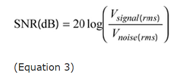
SNR is a comparison of the noise to be expected with respect to the measured signal. The noise measured in an SNR calculation doesn't include harmonic distortion but does include quantization noise (an artifact of quantization error) and all other sources of noise (for example, thermal noise).
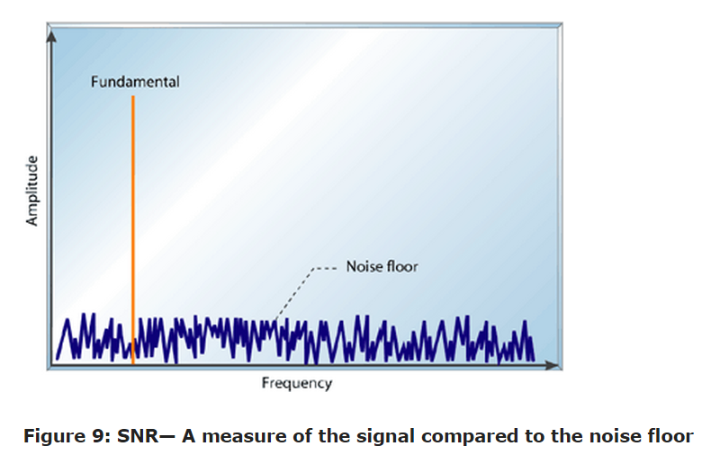
This noise floor is depicted in the FFT plot in Figure 9. For a given ADC resolution, the quantization noise is what limits an ADC to its theoretical best SNR because quantization error is the only error in an ideal ADC. The theoretical best SNR is calculated in Equation 4.
SNR(dB)=6.02N+1.76 (4) Where N is the ADC resolution (Equation 4)
Quantization noise can only be reduced by making a higher-resolution measurement (in other words, a higher-resolution ADC or oversampling). Other sources of noise include thermal noise, 1/ƒ noise, and sample clock jitter.
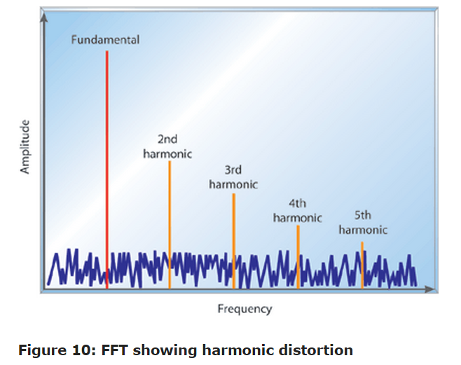
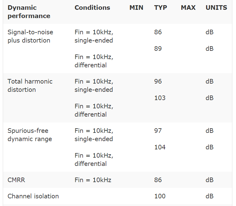
Harmonic distortion
Nonlinearity in the data converter results in harmonic distortion when analyzed in the frequency domain. Such distortion is observed as "spurs" in the FFT at harmonics of the measured signal as illustrated in Figure 10.
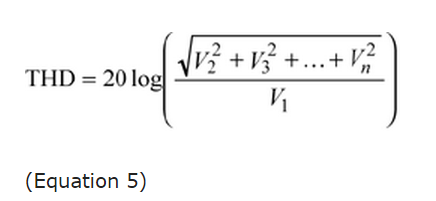
This distortion is referred to as total harmonic distortion (THD), and its power is calculated in Equation 5.
The magnitude of harmonic distortion diminishes at high frequencies to the point that its magnitude is less than the noise floor or is beyond the bandwidth of interest. Data sheets typically specify to what order the harmonic distortion has been calculated. Manufacturers will specify which harmonic is used in calculating THD; for example, up to the fifth harmonic is common (see the example ADC specification in Table 1).
Table 1: Example: Silicon Labs C8051F060 16-bit ADC electrical characteristics
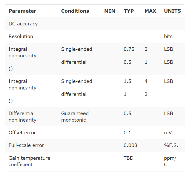
Reading ADC spec numbers
The ADC specifications posted in data sheets serve to define the performance of an ADC in different types of applications. The engineer uses these specifications to define if, how, and in what way the ADC should be used in an application. Performance specifications can also be a guarantee that an ADC will perform in a certain way. If a specification is labeled as a maximum or minimum, this is implied. For example, in the ADC specification shown in Table 1, the data sheet excerpt gives an INL error maximum of 1 LSB. This should mean the manufacturer has tested the ADC and is stating that INL error should not be greater or less than 1 LSB. Besides minimum and maximum, specifications listed as typical are also given. This is not a guarantee but simply represents typical performance for that ADC. For example, if a data sheet specifies 2 LSB INL in the "Typical" column, there's no implied guarantee that the engineer won't find the ADC with higher INL error.
Though a typical number is not a guarantee, it should give the designer an idea of how the ADC will perform, since these numbers are generally derived from the manufacturer's characterization data or are expected by design. Typical numbers are more helpful when the manufacturer gives the standard deviation from the mean of the tested specification. This gives the engineer more information on how the ADC's performance can be expected to deviate from the numbers posted as typical. Keep this in mind when comparing ADC data sheets, especially if the specification is critical to your design. An ADC with a typical 2 LSB INL may yield higher INL error than expected, making a 12-bit ADC effectively a 10-bit ADC—caveat emptor!

 浙公网安备 33010602011771号