Training JTAG Interface
For most embedded CPU architecture implementations, the JTAG port is used by the debugger to interface the chip for debugging one or more cores.
The normal user will probably not need to know details of the JTAG implementation unless there is a need
to debug several daisy-chained JTAG TAP controllers or to access special test functions or configurations
via JTAG that are not implemented in the debugger software.
JTAG is the name used for the IEEE 1149.1 standard entitled Standard Test Access Port
and Boundary-Scan Architecture for test access ports (TAP) used for testing printed circuit boards (PCB) using boundary scan.
JTAG is the acronym for Joint Test Action Group, the name of the group of people that developed the IEEE 1149.1 standard.
The functionality usually offered by JTAG is Debug Access and Boundary Scan:
Debug Access is used by debugger tools to access the internals of a chip making its resources and functionality available and modifiable,
e.g. registers, memories and the system state.
Boundary Scan is used by hardware test tools to test the physical connection of a device,
e.g. on a PCB.
Although the TAP (Test Access Port) access itself is generic for all architectures, the functionality implemented behind JTAG is different for each device.
The following chapter explains all necessities for accessing a JTAG TAP. For a complete description of JTAG see the IEEE 1149.1 standard.
JTAG is defined as a serial communication protocol and a state machine accessible via a TAP.
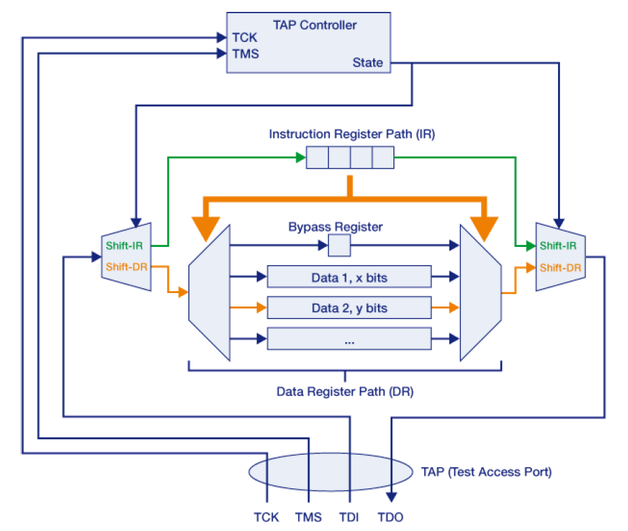
The DTAB (Debug and Test Access Block) is implemented on the target chip as a “passive” device that never sends data without request.
The DTAB mainly consists of the following

The TAP (Test Access Port) with its physical connections (signals) to the external world.
The TAP Controller (a 16-state state machine).
One IR (Instruction Register) and several DRs (Data Registers).
The Debug Bus for communication with the on-chip debug logic.
The TAP defines the interface between the DTAB and the debug tool.
The JTAG Port is the physical connector on the PCB where the debug cable is plugged.
The IEEE standard defines the following TAP signals,
used for the serial communication and driving the TAP controller (JTAG state machine):

The TMS and TDI line are sampled by the DTAP on each rising edge on the TCK line.
The TDO line changes its value after a falling edge on the TCK line.
Instruction and Data Registers
The functionality of the DTAB is accessible via different instructions stuffed into the Instruction Register.
By loading an instruction, the corresponding Data Register is selected for access,
providing and/or accepting data according to the selected instruction.
Only a few instructions are defined by the IEEE standard, and only a few of them are mandatory,
the BYPASS instruction (mandatory) for use in daisy-chained multi-core configurations
IDCODE instruction (not mandatory) for identifying a device
Unused instruction codes can be freely implemented by the device manufacturer.
The width of the IR is not specified by the JTAG standard but needs to be the same for all instructions of a specific device.
Since the DR is selected according to the loaded instruction the DR width is variable.
The following schematic shows the connection of the input signals
with the DTAB and the selection of the Data Register depending on the content of the Instruction Register:
The IEEE standard defines a 16-state state machine called the TAP controller to control several actions:
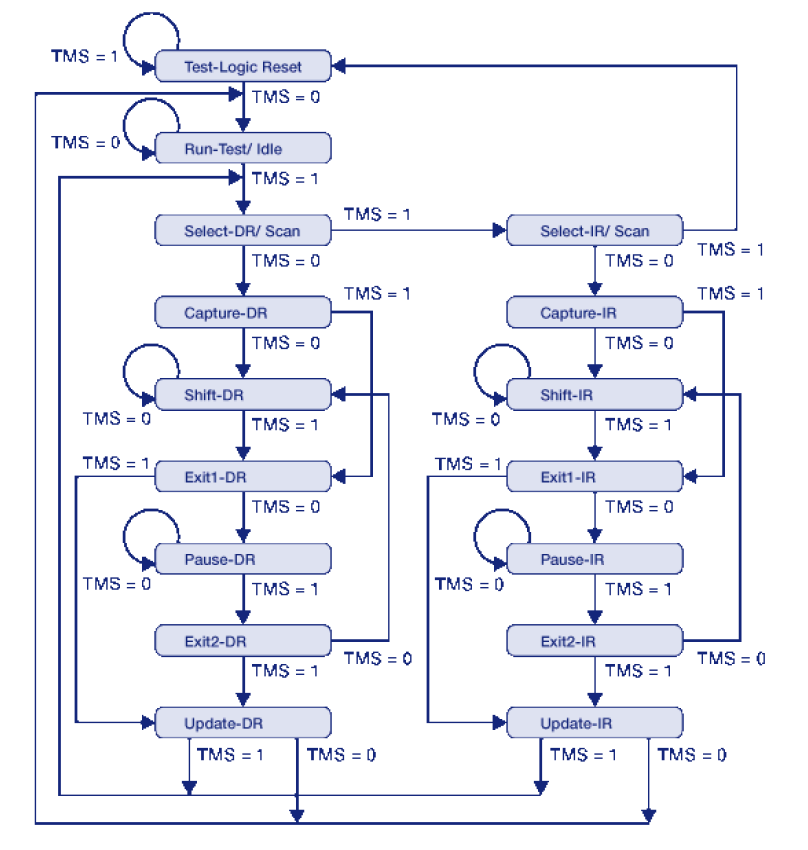
Each state of the TAP controller can be reached by a sequence of bits transmitted via the TMS line depending on the current state.
Normally a DR or IR shift access starts from the pause parking position,
changes to one of the shift states where data is transmitted and ends up in the pause parking position again.
Pause parking position: state the TAP controller holds while waiting for the next shift operation.
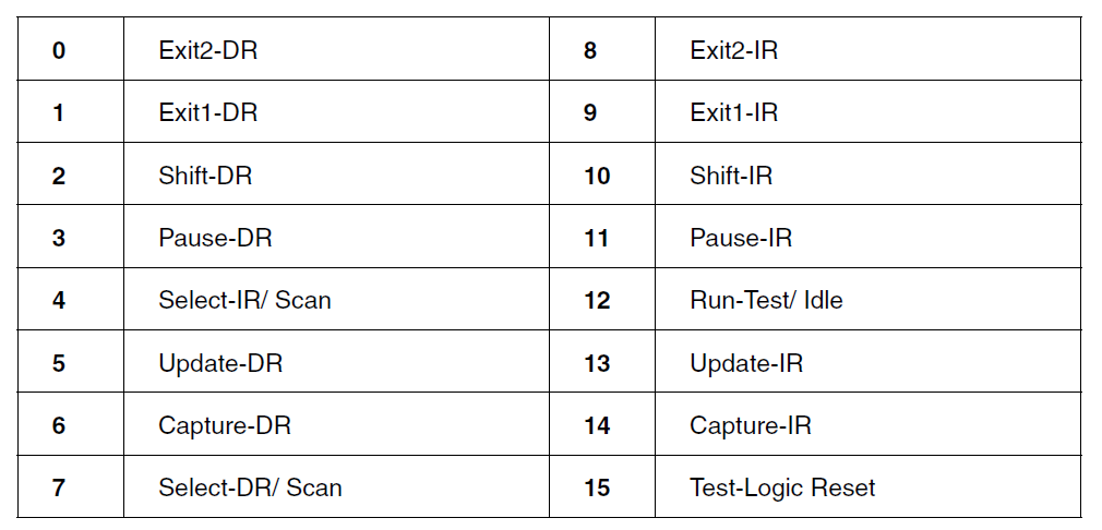
The following states of the TAP controller are of importance:
Test Logic Reset
sets the Instruction Register to its reset value (IDCODE or BYPASS).
This state can be reached from any other state by shifting five times “1” on TMS.
Some CPUs do also reset the DTAB and/or the on-chip debug logic when this state is entered.
As a result an active debug connection might get lost, if this state is driven by a PRACTICE script or a custom application.
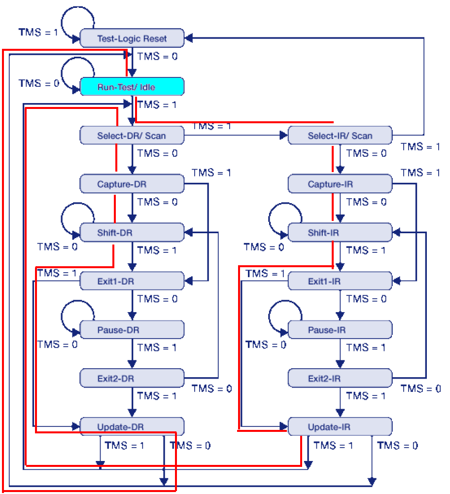
Run-Test/ Idle and Select DR-Scan are used by most debuggers as pause parking position.
In the Shift-IR state the debug tool shifts an instruction into the Instruction Register.
The instruction is activated once the TAP controller reaches the Update-IR state.
In the Shift-DR state the debug tool shifts data to/from the Data Register selected by the currently loaded instruction.
The debug tool communicates with the DTAB by reading and/or writing IRs and DRs.
The debug tool first drives the TAP Controller to the Shift-IR state to write the appropriate instruction to IR.
Then it drives to the Shift-DR state where the DR can be read or written.
Once the Update-DR state is reached, the processing of DR is started, e.g. the data contained in DR is forwarded to the on-chip debug system.
The following example shows how the chip ID code is read on a TriCore processor
(IR: 8 bits, IDCODE DR: 32 bits)
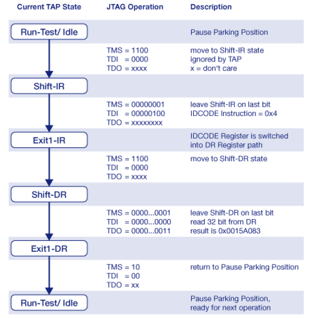
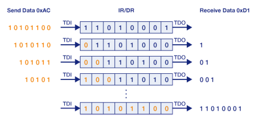
Reading or writing the IR or DR is performed bitwise from LSB to MSB. With every bit shifted into the TAP controller via TDI,
the contents of DR is rightshifted one bit, providing the LSB on TDO.
Shifting in a Daisy-chained Multi-TAP Solution
The TAP controllers of all DTABs are synchronized.
So when transmitting data in Shift-IR and Shift-DR states this means that the Instruction- and Data Registers are chained, too.
Communication with all DTABs simultaneously is not possible
since the connected debuggers all have different tasks to do and so have an individual communication with their core.
Instead only one debugger at a time communicates with one single DTAB,
by loading the Instruction Registers of all other DTABs with the BYPASS instruction (“ignore” mode).
Loading the BYPASS instruction into the Instruction Register will switch the Bypass Register into the Data Register path:
• The JTAG standard defines the BYPASS instruction to consist of “1”s only.
In case the width of the Instruction Register (IR-width) is 4 bit, the JTAG instruction is 0xf,
in case IR-width is 7 bit, the BYPASS instruction is 0x7f.
• The Bypass Register must be a 1-bit register and is preloaded with “0” in the Capture-DR state.
So depending on the position of the DTAB to be addressed,
the Instruction-/Data-Registers of the other DTABs have to be filled with BYPASS instructions, respectively “bypass” bits.
On the following pages an example chip is used, which provides a chain of three DTABs (one TAP each):
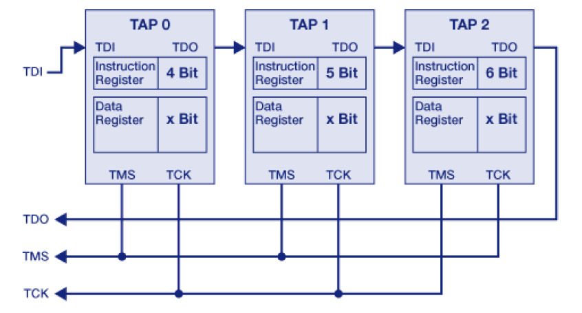
The picture below shows the Instruction/Data Registers if TAP1 is accessed.
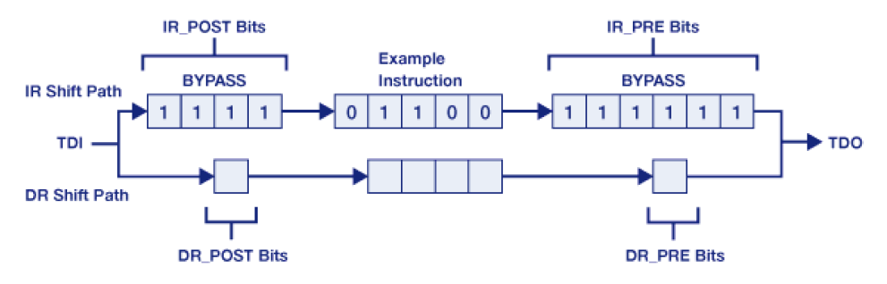
Remember that shifting is performed from LSB to MSB, so in case of an IR shift,
the BYPASS instruction(s) of the TAP(s) after the addressed TAP are shifted in first.
Accordingly these bits are called IR_PRE bits.
The BYPASS instructions of the TAP(s) before are shifted in last so these bits are called IR_POST.
The same applies to the DR path with DR_PRE and DR_POST.
On embedded designs with several TAPs the signals can be chained on board level, so only one common debug connector is required.
This saves space and costs. In case the TAPs are already connected on-chip this also saves pins.
In case a single debugger hardware handles access to all cores under debug,
advanced debug features such as the synchronous multi-core start can be implemented more performant.
The tool must be able to address its core within the TAP chain (multi-TAP capable),
and it must be able to share the JTAG port with other tools.
Because all IRs need to be accessed for shifting instructions,
the complete TAP chain can only be as fast as the slowest TAP thus reducing performance of faster TAPs.
This is especially the case in designs with a return clock (RTCK), e.g. DTABs from ARM.
The connection of the JTAG signals as well as the on-board or on-chip routing must be handled with care to avoid electrical interference,
e.g. by interference of reflections at the end of branch lines.
For handling a multi-TAP system, needs to know only few details about the chain:
• IR_POST is the sum of the IR-width of all TAPs between the TDI pin of the debug connector and the addressed TAP.
• IR_PRE is the sum of the IR-width of all TAPs between the addressed TAP and the TDO pin of the debug connector.
• DR_POST usually is the sum of the bypass registers of all TAPs between the TDI pin of the debug connector and the addressed TAP.
• DR_PRE usually is the sum of the bypass registers of all TAPs between the addressed TAP and the TDO pin of the debug connector.
• TAP State is the neutral parking position where a host instance hands over control of the JTAG chain to another host instance or another debug tool.
The following code are available for the neutral parking position:

 浙公网安备 33010602011771号