STM32F4: Generating parallel signals with the FSMC
STM32F4: Generating parallel signals with the FSMC
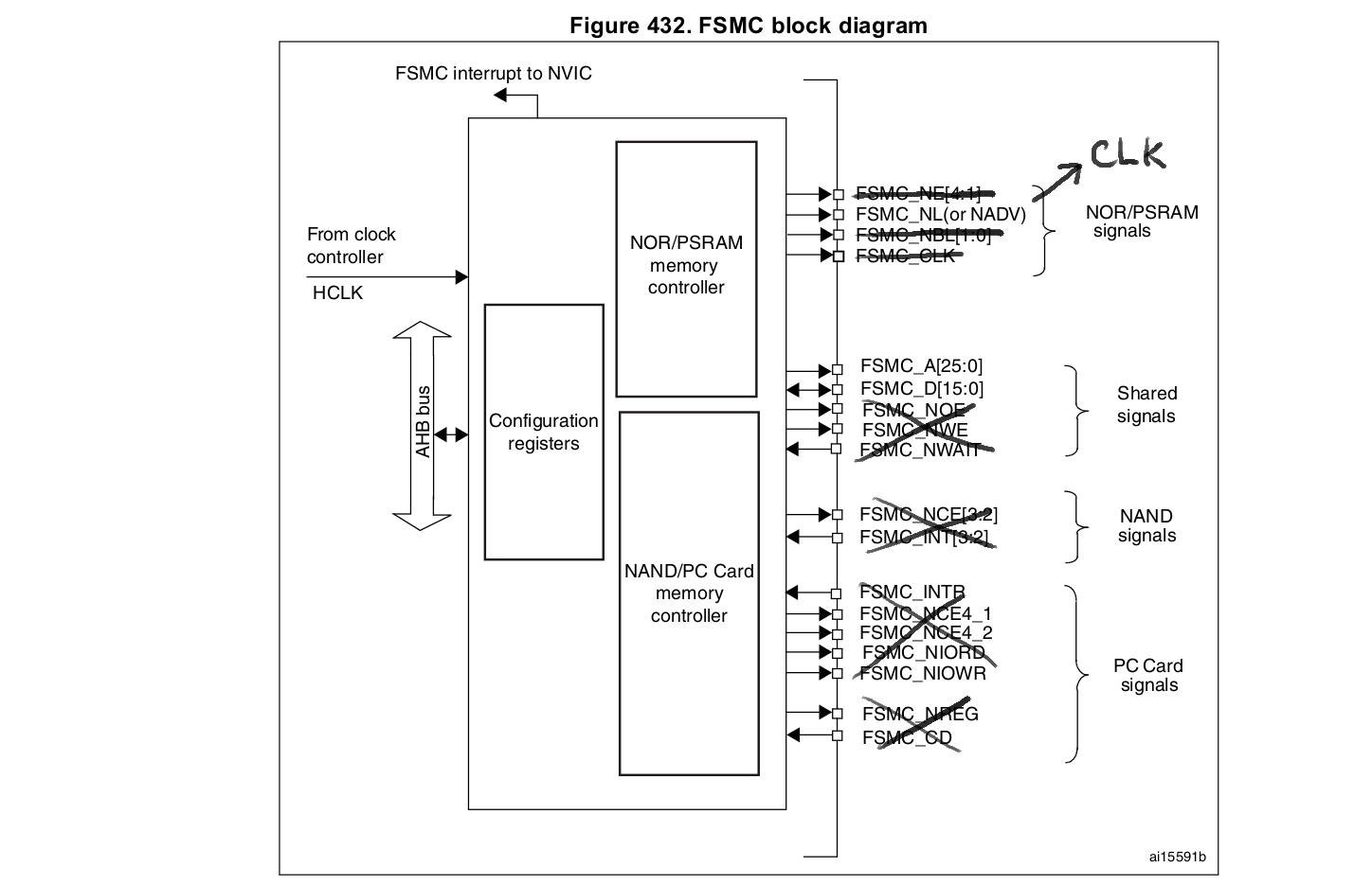
The goal: The memory controller can be used to generate a "generic" 16-bit parallel data stream with clock. Address generation will be disregarded, as well as other control signals dedicated to memory chips.
It must be noted that the STM32F40x and STM32F41x have the FSMC (static memories), while theSTM32F42x and STM32F43x have the FMC (static and dynamic memories). The differences between the two concern the support of SDRAM (dynamic RAM), address and data write FIFOs (both data and address, instead of data only for FSMC, and 16-word long instead of 2-word long only for FSMC), and the 32-bit wide data bus for FMC (See [1]).
Set pins (1st attempt)
Only data bus FSMC_D[15:0] and clock FSMC_CLK will be used (set as alternate function). The other pins are set as standard GPIOs (general purpose output).
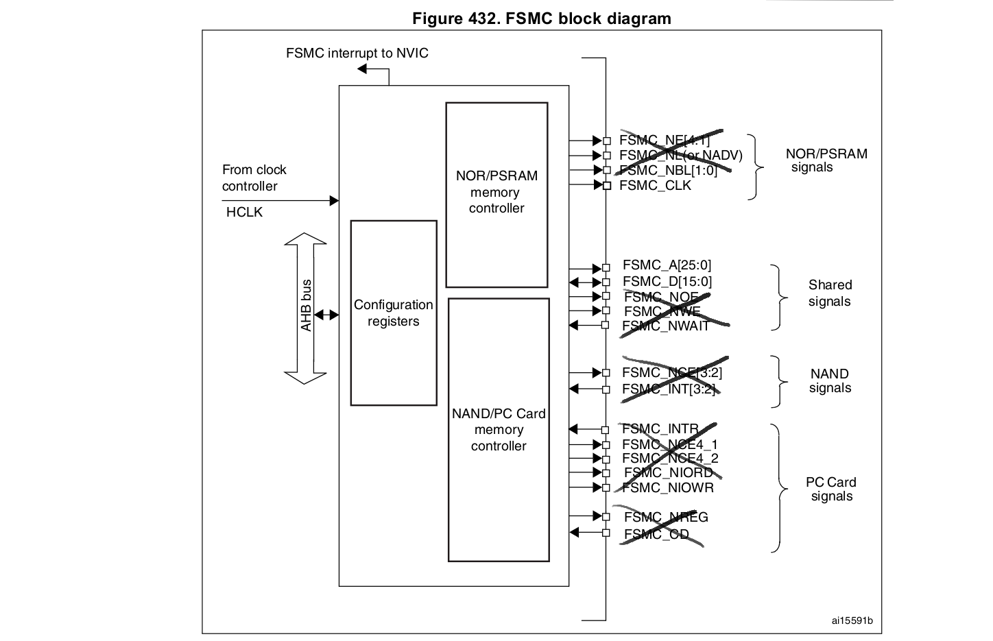
FSMC is alternate function 12 according to the datasheet (See "Table 9. Alternate function mapping" in [2]).
/* PD: 0, 1, 3, 8, 9, 10, 14, 15 -> alternate function (0b10) */
GPIOD->MODER = 0xA56A559A;
GPIOD->AFR[0] = 0xCCCCCCCC; /* FSMC = AF12 (0xC) */
GPIOD->AFR[1] = 0xCCCCCCCC;
/* PE: 7, 8, 9, 10, 11, 12, 13, 14, 15 -> alternate function (0b10) */
GPIOE->MODER = 0xAAAA9555;
GPIOE->AFR[0] = 0xCCCCCCCC;
GPIOE->AFR[1] = 0xCCCCCCCC;
FSMC setup/init (1st attempt)
Be careful of the the wicked register map documentation of the FSMC block:
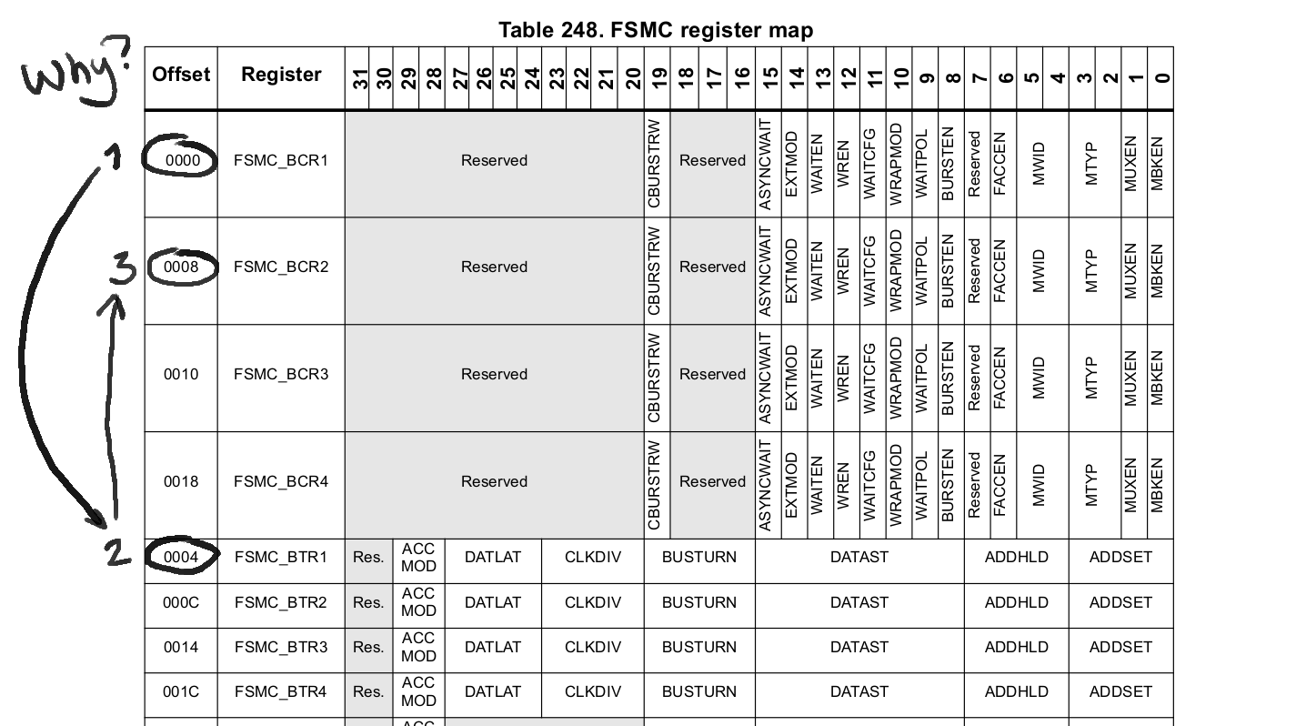
This is very misleading, since all other table are ordered as found in memory, but not here.
/* PSRAM, synchronous (burst), non-multiplexed */
/* control register */
FSMC_Bank1->BTCR[0] = FSMC_BCR1_CBURSTRW | FSMC_BCR1_WAITPOL | FSMC_BCR1_BURSTEN | FSMC_BCR1_MWID_0 | FSMC_BCR1_WREN | FSMC_BCR1_MTYP_0 /* PSRAM */ | FSMC_BCR1_MBKEN;
/* timing register */
FSMC_Bank1->BTCR[1] = FSMC_BTR1_CLKDIV_1 /* div 3 */ ;
It is noticable that the timing are all set to 0, except the clock.
Result (1st attempt)
The code writing to the FSMC is using an array and simulate a sequencial memory request, in order to take advantage of the burst mode.
volatile uint16_t* fsmc = (uint16_t*)0x60000000;

for(uint32_t i=0; i<(sizeof(bitstream_bin)/2); i++) {
        uint16_t w = ((uint16_t*)bitstream_bin)[i];
        fsmc[i] = w;
}
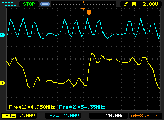
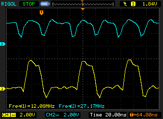
The clock is ~54MHz, but the maximum clock is HCLK/2 = 168/2=84MHz. Unfortunately, my oscilloscope is too slow for this.
At least, 4 clock cycles are required to write one data. Data latency (DATLAT lowest value is 2). There is one cyle to give the address, two cyle of latency, one cyle for give the data.
At max FSMC speed (~84MHz), after dividing the clock by 4, the 16-bit parallel transmission would only be ~20MHz.

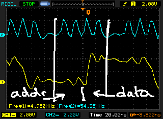
Bursts are possible up to 32 bits (two 16-bit data words). When using this feature, two data words are send for each address, hence more data is sent, but the clock is hard to use: 3 ticks for the (empty) address, 1 tick for the first data, 1 tick for the second data (5 cycles for 2 data, ~30MHz max).
Set pins (2nd attempt)
/* PD: 0, 1, 8, 9, 10, 14, 15 -> alternate function (0b10) */
GPIOD->MODER = 0xA56A555A;
GPIOD->AFR[0] = 0xCCCCCCCC; /* FSMC = AF12 (0xC) */
GPIOD->AFR[1] = 0xCCCCCCCC;
/* PE: 7, 8, 9, 10, 11, 12, 13, 14, 15 -> alternate function (0b10) */
GPIOE->MODER = 0xAAAA9555;
GPIOE->AFR[0] = 0xCCCCCCCC;
GPIOE->AFR[1] = 0xCCCCCCCC;
/* PB: 7 -> AF */
GPIOB->MODER = 0x55551555;
GPIOB->AFR[0] = 0xCCCCCCCC;
GPIOB->AFR[1] = 0xCCCCCCCC;
FSMC setup/init (2nd attempt)
/* NOR flash, asynchronous, multiplexed */
/* control register */
FSMC_Bank1->BTCR[0] = FSMC_BCR1_WREN | FSMC_BCR1_FACCEN | FSMC_BCR1_MWID_0 /* 16-bit */ | FSMC_BCR1_MTYP_1 /* NOR flash */ | FSMC_BCR1_MUXEN | FSMC_BCR1_MBKEN;
/* timing register */
FSMC_Bank1->BTCR[1] = FSMC_BTR1_CLKDIV_0 | FSMC_BTR1_DATAST_0 | FSMC_BTR1_ADDHLD_0 | FSMC_BTR1_ADDSET_1;
Result (2nd attempt)
We want to use the NADV signal as a new clock CLK.
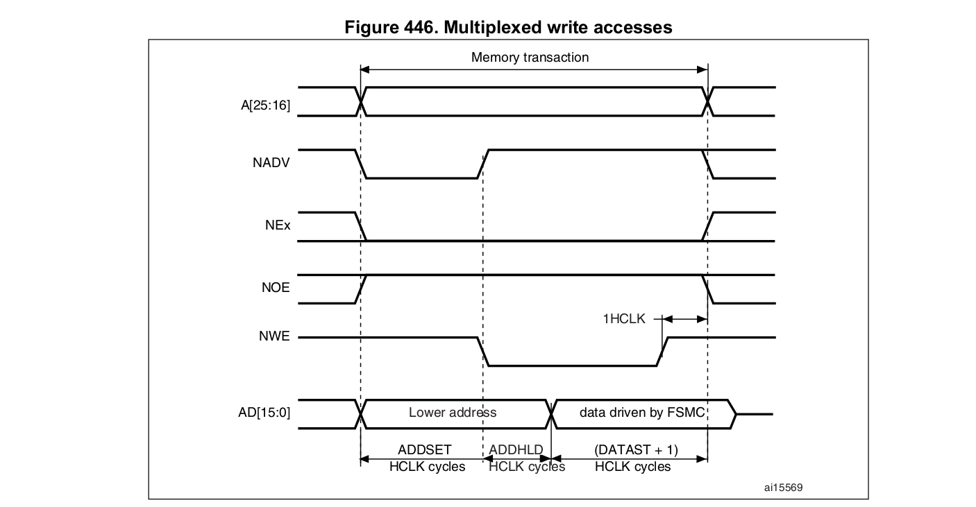
volatile uint16_t* fsmc = (uint16_t*)0x60000000;
uint16_t w[] = {
        0xFFFF, 0x0000, 0xFFFF, 0x0000,
        0xFFFF, 0x0000, 0xFFFF, 0x0000};

for(uint32_t i=0;i<8;i++) {
        fsmc[0] = w[i];
}
We write to the same address in order to force a new memory transaction and cycle NADV.
The problem is that the data bus is updated after the positive edge of the NADV "clock". This issue can be overcome by multiplexing the address and data bus and put the data value as address. The ADDSET value is also increased in order to have a more balanced clock (ADDSET=3).
for(uint32_t i=0;i<8;i++) {
        uint16_t v = w[i];
        fsmc[v] = v;
}
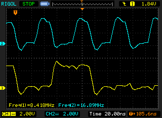
Unfortately, the overall clock speed decreased because the address "trick".
Conclusion
A "nice looking" 16-bit parallel signal with clock can be generated at approx. 16MHz using the memory controller (FSMC) in asynchronous NOR Flash mode. 20MHz can be achieved with an external clock divider (div 4) in synchronous PSRAM mode. If the clock edge can be aligned with the data edge, 27MHz is possible from SRAM.
Note: the FMC (Flexible Memory Controller, also supporting SDRAM) in SDRAM mode can generate a synchronous burst of one data per clock. In this case, 84MHz is possible in theory. I haven't the hardware to test it.

 浙公网安备 33010602011771号