Open Source Universal 48 pin programmer design
http://www.edaboard.com/thread227388.html
Hi, i have designed a 48 pin universal programmer but need help finishing it off, is anyone up for the challange?
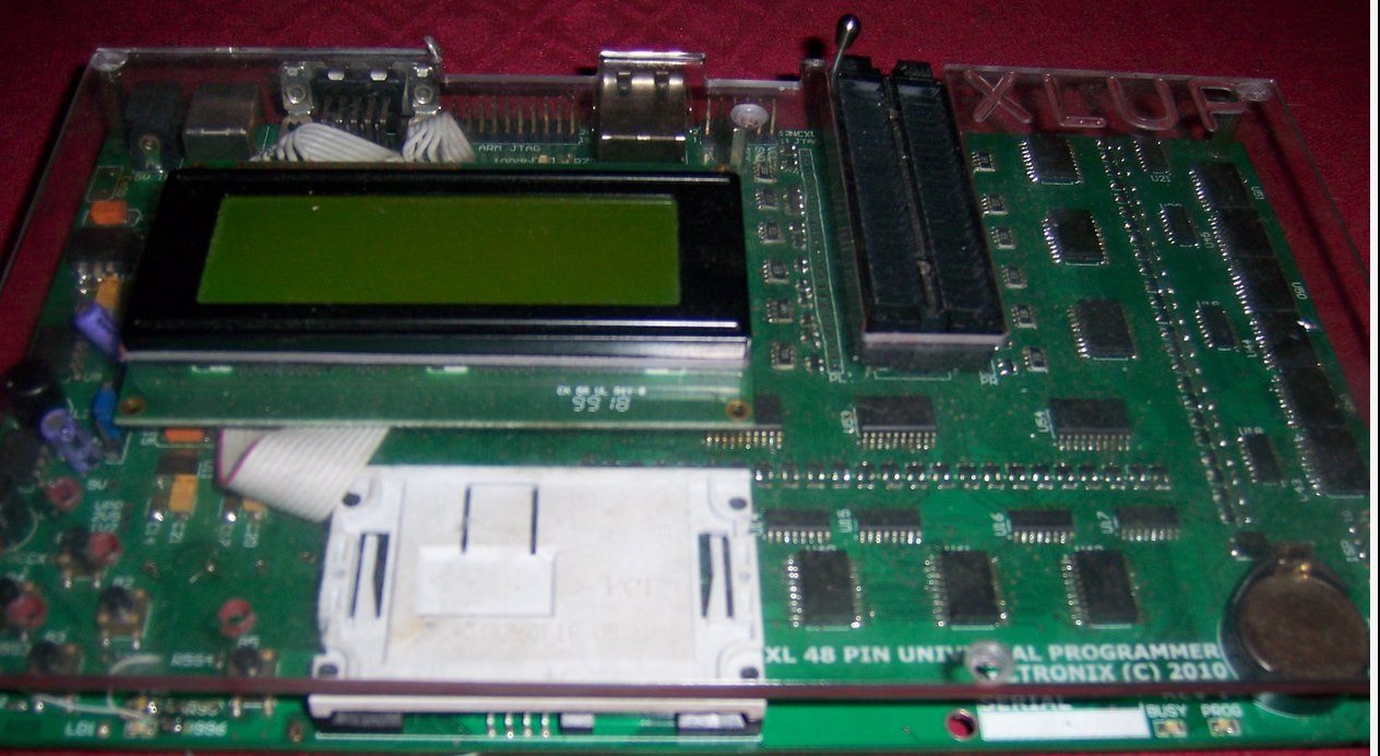
Programmer info:
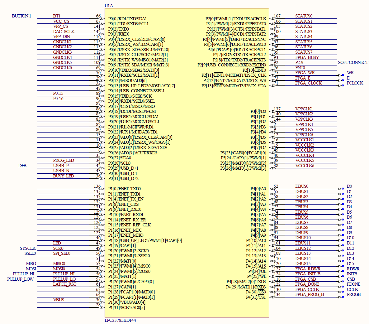
LPC2388 ARM7TDMI CPU with USB
2XDC/DC Converters
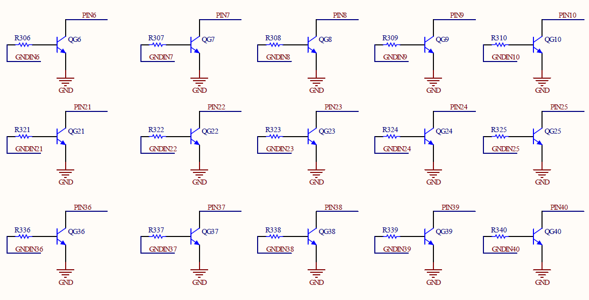
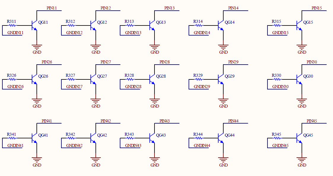
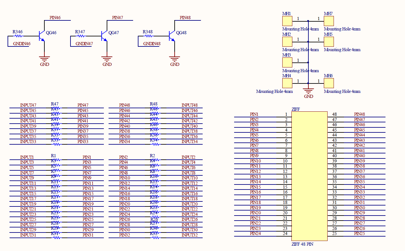
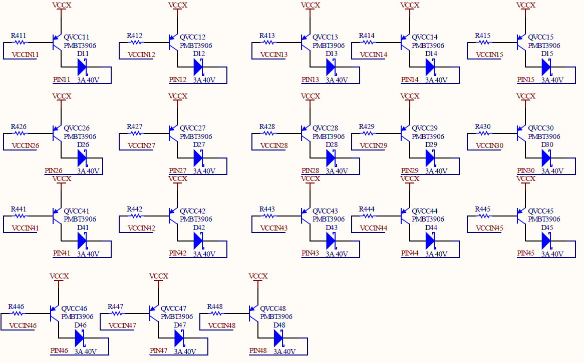
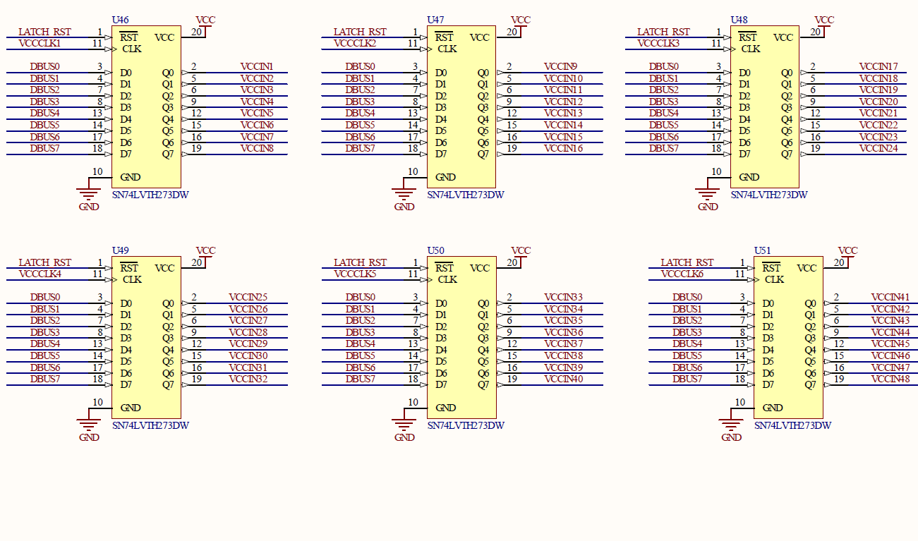
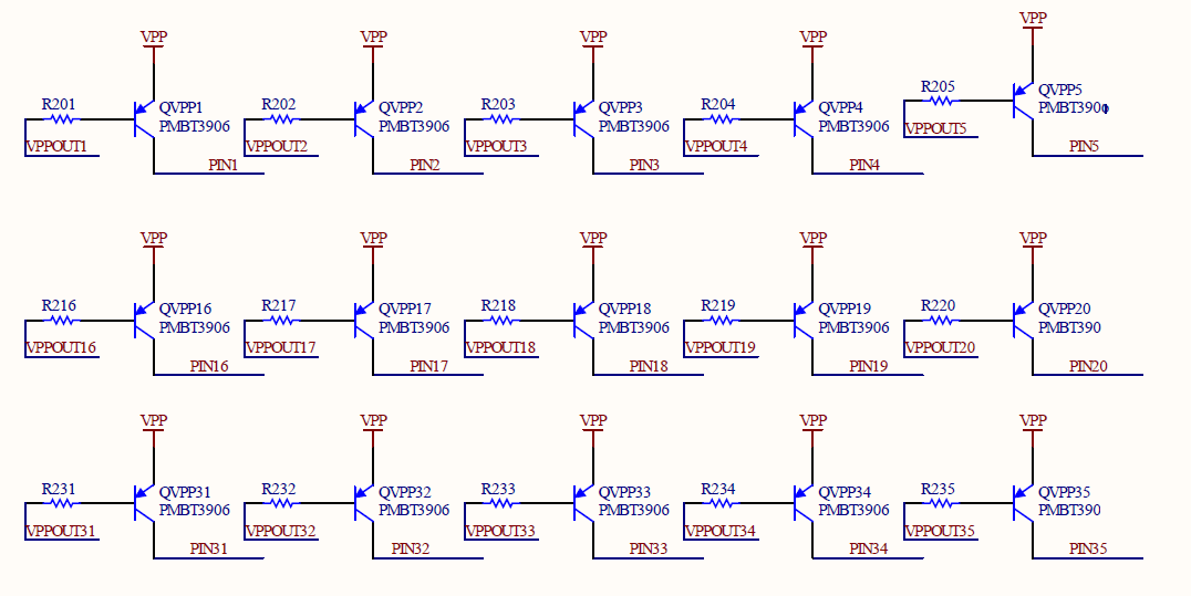
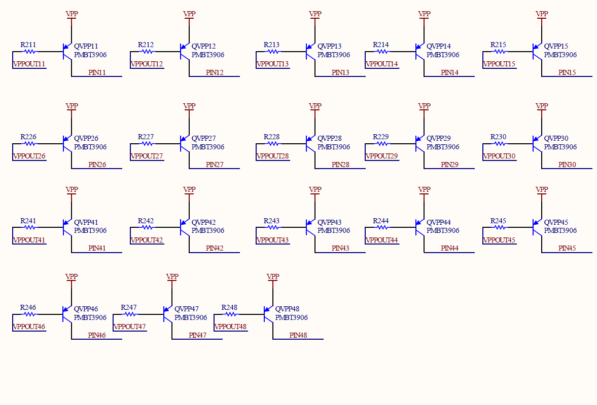
48 universal pin drivers which can be either GND/VCC/VPP/HI,LO/CLOCK/INPUT
Smart card interface
ISP socket which is used for JTag for FPGA's/CPLD/ARMs Anything JTag... /serial programming devices mounted on a board Pic's/AVR's etc/In car Dashboards/ECU's etc
USB Interface
Ethernet Interface
SD card
LCD
Serial interface
Buttons/switches lights etc
JTAG For ARM
JTAG for FPGA
Soft JTAG for FPGA
This is really a massive project and has taken me a while to get this far, i think i need help to finish it.
The software is written in delphi:


USB Uses CDC So can be used on any PC.
So far i can read and write to all pins fine, program the FPGA, etc
There are three parts to the programmer.
Firmware:
Written in C using Keil compiler.
FPGA:
Designs are done in Altium.
PC Software:
Written in Delphi 7
I am very good with the firmware, and not bad with the FPGA, the PC software is not good for me...
I want the software, fpga designs and the firmware to be OPEN SOURCE, this was the idea behind it, as you cannot by a good true universal programmer for less than around £500 i thought it would be a good project to undertake, with the added benefit of a smart card programmer and ISP it should be a good device, and hoping to ship it for less than £100
So if you are up for a challange let me know......
Many Thanks....
Picman....
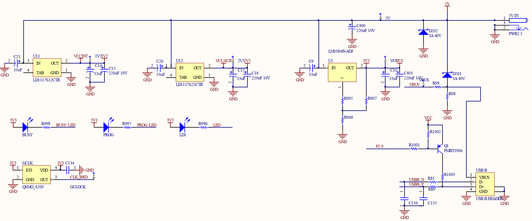
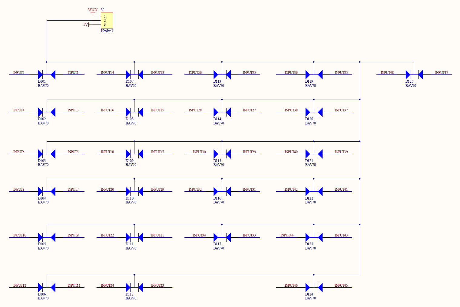
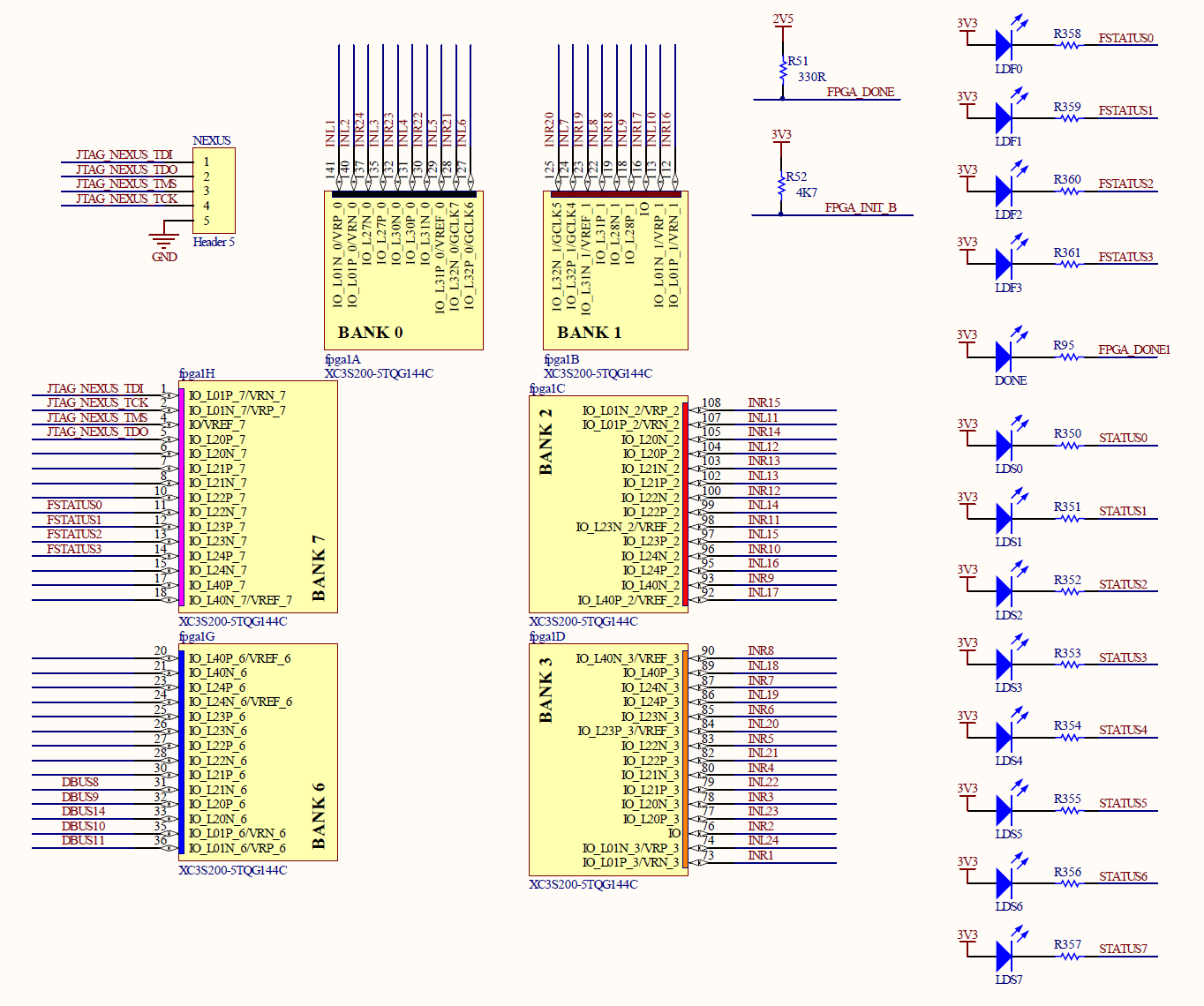
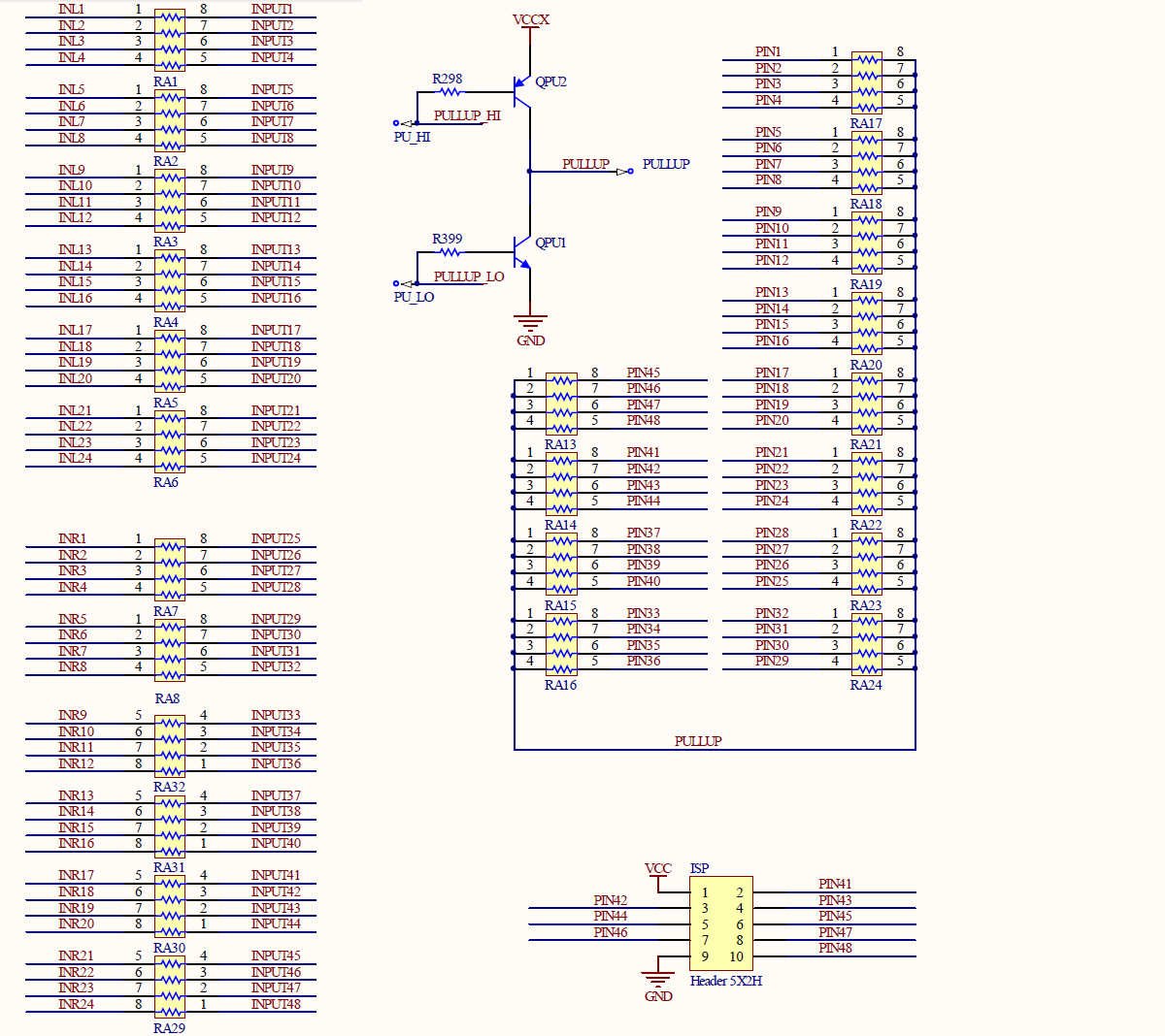
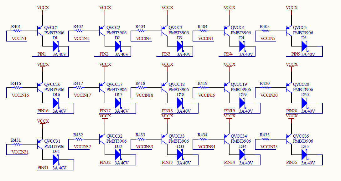
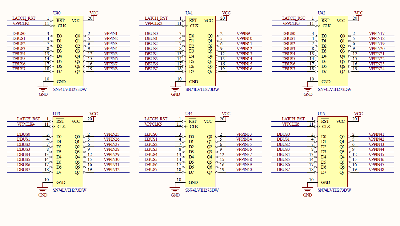
Programmer Schematics....
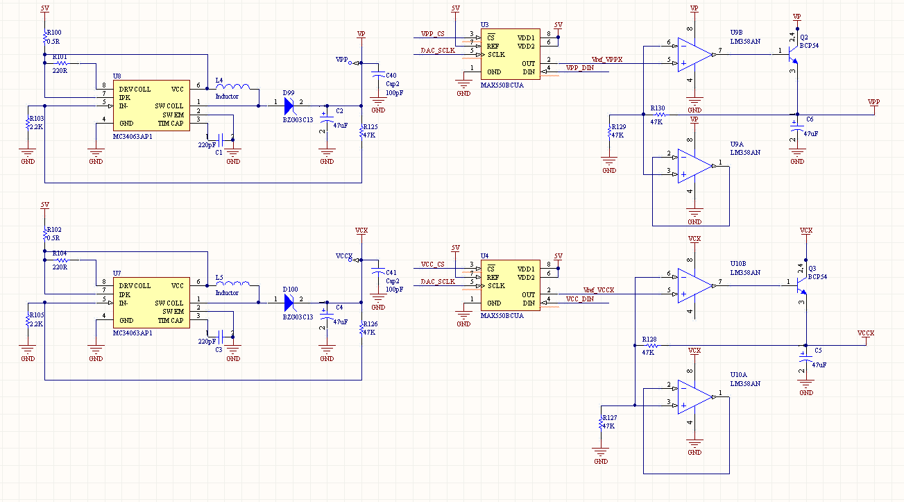
The PSU for VCC and VPP need changing does not work too well, but i think it would be good to only need the 5V from the USB to power the programmer, so DC/DC converters are needed to get VPP.
The FPGA is key to the programmers functionallity, even if you just use it to route pins to the micro so using it as a pin matrix. but you can do a lot more with it there, as it is, it will program most programmable devices on the market.
I am fine with coding the verilog for the fpga anyway..
What about replacing fpga with cpld? You can get those in packages like qfp44. This would somewhat reduce difficulty of assemblying it at home.
Unfortunately there are 48 IO's from the ziff so it needs a larger package than the 44 pin, i have assembled 2 of these at home an both work fine, just takes a little time. also the ARM is 144 pins and most pins are used.
Anyway the basic idea will be to sell the boards already made, but open source the software, but i do see where you are comming from for the development.
Having 200K gates also opens up a lot more potential for doing some clever things in the fpga, and freeing the CPU from a lot of tasks. For instance a logic analyzer.....
If idea is to sell the board already made than large footprint FPGA is fine.
A logic analyzer is also a nice idea, but for it to have good parameters you need an external RAM chip, because the bandwidth of USB is insufficient for analyzing high speed signals.
I think that it would be nice if your device was able to switch between different compatibility mode. I mean that you could set it up to work like pickit 2 and be able to use it from MPLAB. Or set it up to work like STK500 and be able to use it from AVR studio. That would increase functionality creatly, because most people find it far more convenient to be able to operate programmer/debugger straight from IDE.
I realize that it would need enormous amount of coding and reverse engineering, but having a universal programmer with IDE compatibility would be very nice.
What would you use the IDE for? If its programming the ARM then there is already an IDE which i use called KEIL.
No, I mean the IDE which u will be using to develop software that you will later download into some device using this programmer. Or maybe I got the purpose of this device wrong?
To achieve 48 pin drive all, the fpga haved more than 48 io's and Dynamic reconfiguration
Firmware must be prepared to understand the hardware architecture, and sometimes have to modify the hardware design to suit the software development
I do not know the hardware architecture in the case, there is no other thing that programmers can do
If you want to do open source, then this is a must. If you do the programmer development platform is to provide a schematic
my development :
windows 2003
keil 8.16a
visual c++ 6
Yes a Schematic will be provided, also the interface from the ARM to the FPGA is fixed, so its always the same no matter what device you program.
The purpose of the Programmers is a IC device programmer, like Datamans Dataman 48UXP Universal Programmer
But it can do more because it has a smart card slot, and an ISP plug and also can use ethernet and usb and serial, plus loads more....
It can also be used as a JTAG programmer/debugger etc....
the Programmer‘s vccx and vpp do what needs to be improved
and head3 ,How to use it? do Hand?
Pullups/pulldowns work ok, VCC and VPP need to be redesigned, im not happy with them at the moment.
Whats Head3?
The power supply for vcc and vpp will be controlled by the ARM so we need some digital 3v3 way of changing the voltages on vcc and vpp.
Pullups/pulldowns work ok, VCC and VPP need to be redesigned, im not happy with them at the moment.
Whats Head3?
The power supply for vcc and vpp will be controlled by the ARM so we need some digital 3v3 way of changing the voltages on vcc and vpp.
Ok what voltages can you get on vcc and vpp, what sort of range.. 0..25V and 0..5V???
And what Current?
Do you think it would work fine from 5V from USB?
If so your idea is good...
On the LPC2388 the ARM CPU we only have one DAC, so we would need an external DAC IC for your PSU to work.
Also in you PSU design what about pin 4 on the MC34063? I thought pin 4 was GND and pin 6 was VCC?????
A:
1.
vcp‘s range 1.8~6.8v
vpp’s range 1.8~25V
one step 0.1v
2.By sampling the voltage difference across the resistor to convert current
Programmable reference source and a comparator for protection
Of course, access to and control of current through the operation
3.34063
Use the datasheet of the design
I use the package who have‘nt 6 pin and 4 pin
pin4 gnd
pin6 vcc
Q?Pullups / pulldowns
How it’s work
What is the function in the end
thanks
Pullups are uses as a logic 1.
So to write a 1 to the device being programmed you set the IO pin on the FPGA as HIZ or input, this will allow the Weak pullups to pull the pin to VCCX so putting a logic 1 on the pin.
The point of this is that a logic 1 is always the same as VCCX so if you want to program for example a 2.5V device then as long as VCCX is at 2.5V then the logic 1 will be the same voltage.
If we used the FPGA pin to output a 1 then this would be 3.3v, not good for a 2.5V or 5V or 1.8V device...
Do you understand now?
vcp‘s range 1.8~6.8v
vpp’s range 1.8~25V
one step 0.1v
This sound fine, how many steps has the DAC got?
I think an 8 bit DAC would do fine with 256 steps, 0.2v steps..
I don't think that any IC is that fussy that it needs a resolution better than 0.2V for programming.
So i have found some DACs from Maxim MAX550B that are 8 bit and use a simple SPI serial interface. 8 pin and are 2.5V to 5.5V single supply.
They are also very cheap...
So the new diagram for the PSU would be...
thanks
my programmer‘s vcp is the target chip power supply
Programmable control, can achieve any voltage 1.8 to 6.5v
Q?
Test pin is bad how to achieve it
Test pin is bad how to achieve it ? I don't understand...
Test pin contact is good
Whether short or damage the chip
The chip is inserted upside
These are supported by professional programmers
There voltage rise-time control or increased steepness
??????
I think and think, but did not know there are many
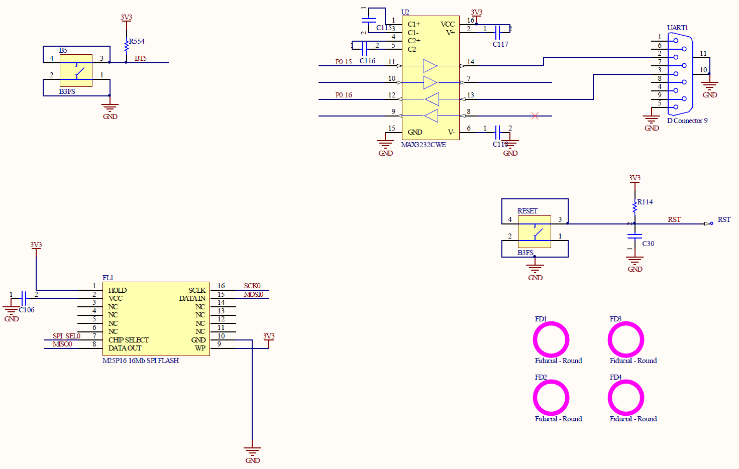
New Schematics
programmer.pdf
Changes:
DAC controlled PSU for VCCX
DAC controlled PSU for VPP
Ethernet and SDCARD removed.
Smartcard Removed.
LEDs added for status on ARM
LEDs added for status on FPGA.
This should make the programmer cheaper but still function the same.
Take a look at the schematics and tell me what you think.
Programmer supports sd card run offline is a good choice
Dot-lcd display would be better
My idea, please refer to


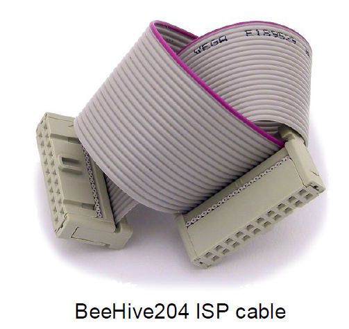
BeeHive204 ISP connector
As ISP connector is used 20 pins connector 2-1634689-0 from TE connectivity or other compatible connector.
ISP connector
20-pin male type with miss insertion lock
6 TTL pindrivers, provides H, L, CLK, pull-up, pull-down; level H selectable from 1.8V up to 5V to handle all (low-voltage including) devices. [ 3 5 7 9 11 13 ]
1x VCCP voltage (range 2V...7V/100mA)
programmed chip voltage (VCCP) with both source/sink capability and voltage sense
1x VPP voltage (range 2V...25V/50mA)
Target system power supply voltage (range 2V...6V/250mA)
ESD protection on each pin of ISP connector (IEC1000-4-2: 15kV air, 8kV contact)

H/L/read driver

RA1 180R,
RA2 1k3,
RA3 22k,
RB1 10k,
RB2 10k,
CC1 1n,
RC1 1k3,
RC2 22k,
RD1 22k,
CE1 1n,
RE1 1k3,
Comment to above picture:
picture C) Connection of pins 15 and 16 when are configured as logical signal needed for ISP
programming
pictures D) E) When pins 15 and 16 are configured as status of LED OK and LED ERROR
picture D) before first action with desired ISP device
picture E) after first action with desired ISP device
Notes: When LED OK or LED ERROR ON (shine), this status is presented as logical H, level
of H is 1,8V - 5V depend on H level of desired ISP device.
When LED OK or LED ERROR OFF (not shine), this status is presented as logical L, level of
L is 0V - 0,4V.
The above mentioned values are provided to understand (and also to exactly calculate) the
value of resistors, which isolate (separate) the programmed chip and target system.
Specification of ISP connector pins depends on the device, which you want to program. You
can find it in the control SW for programmer (PG4UW), menu Device / Device Info (Ctrl+F1).
Be aware, the ISP programming way of respective device must be selected. It is indicated by
(ISP) suffix after name of selected device.
These specifications correspond with application notes published of device manufacturers.
Used application notes you may find on www.elnec.com, section Support / Application
Notes.
Note: Pin no. 1 is signed by triangle scratch on ISP cable connectors.
As ISP connectors are used 20 pins connectors 09185207813 from Harting or other
compatible connector.
Warnings:
Use only attached ISP cable. When you use other ISP cable (other material, length…),
programming may occur unreliable.
BeeHive204 can supply programmed device (pin 1 of ISP connector) and target system
(pins 19 and 20 of ISP connector) with limitation (see Technical specification / ISP
connector).
BeeHive204 apply programming voltage to target device and checks his value (target
system can modify programming voltage). If the programming voltage is different as
expected, no action with target device will be executed.

 浙公网安备 33010602011771号