SAE J1708 DS36277 MAX3444, DS75176B
http://en.wikipedia.org/wiki/J1708
J1708
SAE J1708 is a standard used for serial communications between ECUs on a heavy duty vehicle
and also between a computer and the vehicle.
With respect to Open System Interconnection model (OSI), J1708 defines the physical layer.
Common higher layer protocols that operate on top of J1708 are SAE J1587 and SAE J1922.
The protocol is maintained by SAE International.
Description
The standard defines a 2-wire 18 gauge wire cable that can run up to 130 feet (40 m) and operates at 9600 bit/s.
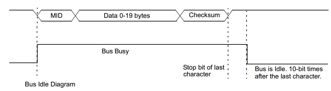
A message is composed of up to 21 characters, unless the engine is stopped and the vehicle is not moving
in which case transmitters are allowed to exceed the 21 byte max message length.
Messages start with a Message ID (MID) character and finish with a checksum at the end.
Characters are transmitted in the common 8N1 format.
The hardware utilized are RS-485 transceivers wired for open collector operation
through the use of a pullup and pulldown of the separate data lines.
Transmission is accomplished by controlling the driver enable pin of the transceiver.
This method allows multiple devices to share the bus without the need for a single master node.
Collisions are avoided by monitoring the bus while transmitting the MID
to ensure that another node has not simultaneously transmitted a MID with a higher priority.
History
SAE J1708, although still widely used, is replaced by SAE J1939 which is a CAN protocol. 
AN-915 Automotive Physical Layer SAE J1708 and the DS36277
The Society of Automotive Engineers (SAE) Recommended Practice J1708
The SAE has defined this recommended practice for serial data communications
between microcomputer systems in heavy duty vehicle applications.
It is also well suited to passenger car applications (as shown in Figure 1) and many non-automotive uses.
The bus is expected to be used for sharing data.
An applications document, like SAE J1587 or SAE J1922, defines the actual data or functions to be transmitted.
SAE J1708 only defines the hardware and basic software.

The physical media is a two-wire bus using 18-gauge twisted pair with a minimum of 1 twist per inch.
The maximum length is intended to be 40m.
A maximum of 20 nodes is specified.
Deviations from this must be carefully analyzed to determine impact on bus performance over the entire operating range.
Each node may access the bus randomly once the bus is idle for a predetermined access time.
If two or more nodes attempt to access the bus at the same time, the contending nodes must arbitrate for the bus.
Arbitration is determined by priority, which is set between 1 (top priority) and 8.
An applications document will reference SAE J1708 and define the priority associated with each message.
Since there can be up to 20 nodes, it is possible for two contending nodes to have the same priority.
When contention exists between two or more nodes, arbitration is determined by the bus access time.
This is the time a node is required to wait before it can attempt to access the bus.
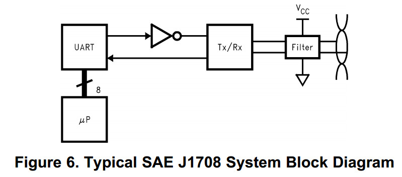
The protocol is consistent with standard universal asynchronous receiver/transmitter (UART) operation.
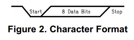
A message consists of a message identification character (MID), a data character(s) and a checksum character.
The total message length should not exceed 21 characters. A character is defined as 10 bits:
the first bit is always the start bit (logic level LOW), followed by eight bits of data and,
the tenth bit is the stop bit (logic level HIGH) (see Figure 2).
The bit timing equates to a baud rate of 9600.
The logic LOW and HIGH levels are encoded as “dominant” and “recessive”, which is described later.
The hardware is defined by the RS-485 standard for its electrical characteristics,
with some exceptions and modifications.
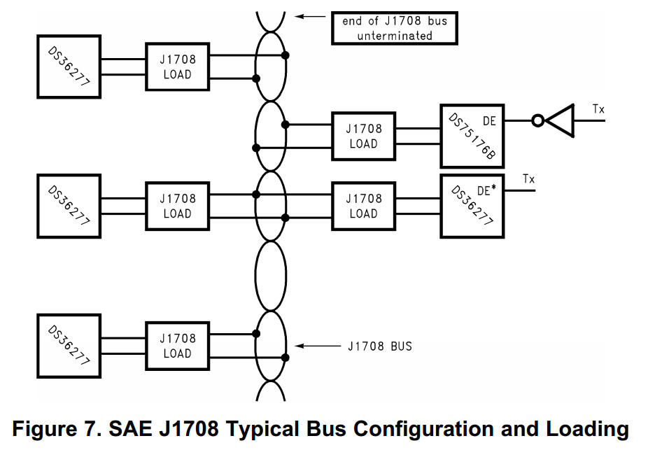
J1708 Bus Loading
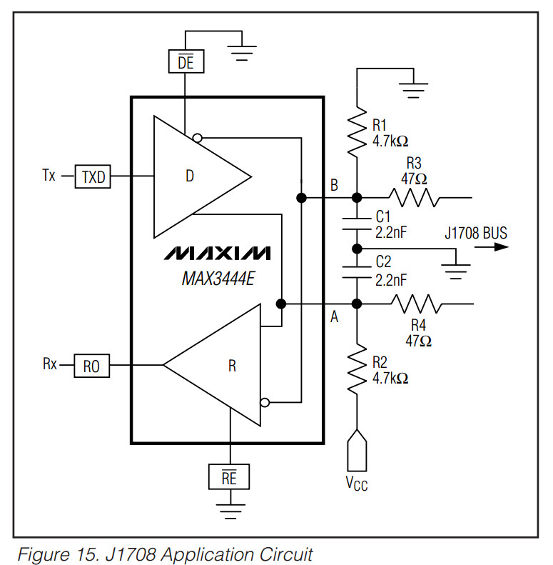
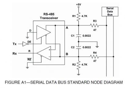
The recommended implementation for a SAE J1708 load is shown in Figure 3 .
The recommended implementation for a SAE J1708 system using a standard RS-485 transceiver,
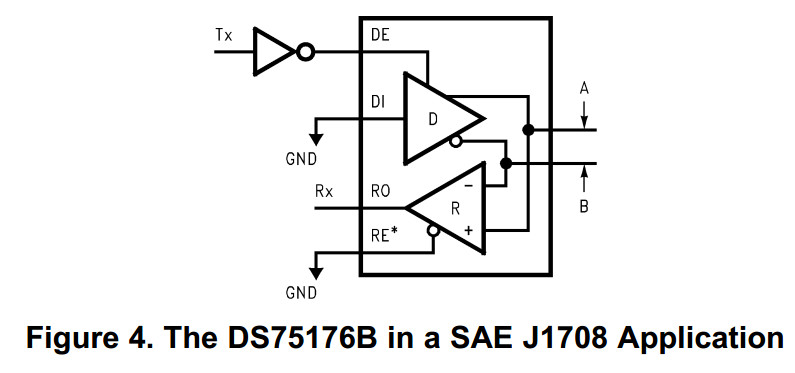
such as the DS75176B (see Figure 4), is shown in Figure 7.
The circuitry between the bus and the transceiver differs from RS-485 and is intended to provide several features:
• R1 and R2 provide the bias for the “recessive” state.
• C1 and C2 combine to form a 6 MHz low-pass filter, effective for reducing FM interference.
• R2, C1, R4 and C2 combine to form a 1.6 MHz low-pass filter, effective for reducing AM interference.
• Since the bus is unterminated, at high frequencies R3 and R4 perform a pseudo-termination.
This makes the implementation more flexible as no specific “termination nodes” are required at the ends of the bus.
The resistor and capacitor values are as follows and are shown in Figure 3:
• Resistor 1 and 2 (R1 and R2)— 4.7 kΩ
• Resistor 3 and 4 (R3 and R4)— 47 Ω
• Capacitor 1 and 2 (C1 and C2)— 2.2 nF
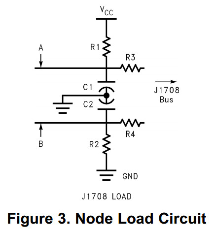

A.1 This circuit utilizes standard RS-485 transceivers (less than or equal to one RS-485 unit load) connected to drive the differential data bus to the logic zero state only (unipolar drive).
In the previous circuit, a standard RS- 485 receiver may be used in place of a transceiver in applications where data need not be placed on the bus (that is, receive only).
A.2 The logic 1 state (also idle state) is controlled by pull-up resistor R1 and pull-down resistor R2.
A.3 The transceiver output impedance, C1 and C2, form the transmit filter for transient and EMI suppression (approximately 6 MHz low pass).
A.4 R3, C1, R4, and C2 form the receive filter for EMI suppression (approximately 1.6 MHz low pass). These parts also form a pseudo line termination at high frequencies.
A.5 The active (high-to-low) transition delay is approximately 0.6 ms at the receiver with two nodes on the bus and 2.3 ms with 20 nodes on the bus.
A.6 The passive (low-to-high) transition delay at the receiver remains at 10 ms with any number of loads on the bus (up to 20).
A.7 The values shown were chosen for use with commercially available RS-485 drivers to provide maximum fan- out, EMI suppression, and bus termination.
Remaining nodes may be in either the powered or unpowered state.
A.8 This method of unipolar drive prevents unresolved contention (logic 0 always wins).
A.9 The resistors shown should be 5% parts to assure sufficient noise margin under worst-case conditions.
R3, R4, C1, and C2 should be balanced within 10% on each side of the data bus to minimize common mode electromagnetic radiation.
Dominant Mode
The drivers used by SAE J1708 are used in a dominant mode application.
The driver's input (DI) is tied LOW and the signal (Tx) to be transmitted is tied to the driver's enable.
The enable (DE) is active HIGH for the DS75176B while the enable (DE*) for the DS36277 is active LOW.
First, this information is very important because this tells us that the driver is only capable of driving LOW.
Therefore, a logic level LOW is encoded as “dominant”.
When the driver is disabled, the bus is pulled high by external bias resistors R1 and R2 (as shown in Figure 3).
Therefore, a logic level HIGH is encoded as “recessive”.
Second, if the driver's enable is active LOW, then you will transmit positive logic.
But, if the driver's enable is active HIGH you will transmit negative logic.
SAE J1708 is only defined for positive logic.
Therefore, to implement a SAE J1708 application using DS75176B, which has an active HIGH driver enable,
an inverter is needed for the driver enable (see Figure 4 and Figure 6 ).
However, the active LOW driver enable pin on the DS36277 saves you an externally needed inverter (see Figure 5).

In the case of a SAE J1708 application, a logic LOW can overwrite a logic HIGH.
Therefore, if contention exists between two drivers with transmitting signals (Tx) in opposite states,
the driver driving the “dominant” state wins.
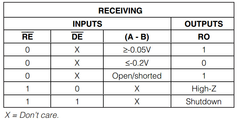
SAE J1708 requires all receivers to listen to every message identification character transmitted to determine if contention exists.
Unlike the driver, the receiver's enable (RE*) is always tied LOW (see Figure 4 and Figure 5).
This means the receiver is always in listen mode (see Explanation of Terms).
The external components shown in Figure 3 provide the necessary bias for a logic High “recessive” state.
SAE J1708 requires no additional external components other than the J1708 load.
This means that no parallel termination can be used at the ends of the SAE J1708 bus.
The required loading also provides failsafe protection.
Features of the DS75176B
The DS75176B offers full compliance with the RS-485 standard and it is compatible with RS-422 and V.11.
The device is available with industrial temperature range.
Additionally, a thermal shutdown circuit protects the device against thermal overstress due to excessive power dissipation.
Furthermore, the receiver has failsafe protection.
However, the receiver's output is only guaranteed to be in a logic HIGH state for an open input line condition.
The receiver also has ±200 mV threshold levels.
The driver has an active HIGH enable while the receiver has an active LOW enable.
Features of the DS36277
The DS36277 is optimized for use with SAE J1708 electrical applications and the device is
still compatible with RS-485, RS-422, and V.11 standards.
Like the DS75176B, the device is available with industrial temperature range.
Also the device includes thermal shutdown protection; plus the receiver has failsafe protection.
Additionally, the receiver has full failsafe defenses that includes shorted and terminated line fault
and conditions as well as open line conditions.
The receiver's output is assured to be in a logic HIGH state for all three line faults and conditions.
The receiver's 0 V to −500 mV threshold provides the protection from shorted line faults.
Unlike the DS75176B, both the driver and the receiver have an active LOW enable.
The DS36277 also has a very rugged ESD structure that allows it to withstand electrostatic discharges
(ESD) up to 7 kV (HBM). The device is also available in SOIC as well as DIP packages.
Conclusions
Selecting an established physical layer such as J1708 can eliminate many of the challenges of designing a serial communications system.
The dominant mode operation allows for a non-destructive arbitration scheme.
J1708 is based on RS-485 electrical specifications and benefits from the ruggedness,
low cost and availability of compliant ICs are already on the market.
The DS36277 transceiver has been optimized for J1708.
It provides failsafe protection against bus faults and eliminates the need for an external inverter.


http://ww1.microchip.com/downloads/en/AppNotes/01230A.pdf
AN1230
SAE J1708/J1587 Communications with the EUSART
The Enhanced Universal Synchronous Asynchronous Receiver Transmitter (EUSART)
FEATURES
The features of the EUSART are as follows:
• Selectable 16-bit Baud Rate Generator mode
• Interrupt on Sync Break character received
• 12-bit Break character transmit
• Auto-baud calibration on Sync character
• Clock polarity select for Synchronous mode
• Transmit polarity select for Asynchronous mode
• Receiver Idle flag
• Receive Shift register empty Status bit during Sleep

J1708 Wiring on a 9 Pin SAE Connector:


 浙公网安备 33010602011771号