NAND Flash memory in embedded systems
参考:http://www.design-reuse.com/articles/24503/nand-flash-memory-embedded-systems.html
Abstract :
This paper presents fundamental information about NAND Flash memory used in Embedded Systems. It discusses various aspects of this storage media such as interface, architecture, error source and error correction as well as software required for building application.
Introduction
Flash memories became very popular in electronic systems. They are used to store program and data information, they allow to update firmware in the field when product is already deployed. They allow to store an immense number of files in a small single chip.
NOR Flash is widely used as a direct replacement for regular ROM memory, the NAND Flash on the other hand is not that popular, maybe due to the different access approach, different interface and specific operation requirements although they are excellent solution when big storage is required. They can store data as well as program information with high data reliability. They can work as a replacement for rotating media storage devices where the latter ones are impractical as in high mechanic shock environments.
History
It was Toshiba which introduced NAND Flash for the first time in late 80s of the last century. It was a consequence of work over Flash technology which led to significant reduction of a single cell size. However, it came at the price of user friendliness. There are no such interface like in NOR or SRAM memories, there is just data bus and a communication protocol to feed commands and data to the memory chip.
Construction
The NAND Flash cell is composed of a single FET transistor equipped with extra gate called floating gate which stores the extra charge with information. The set of transistors is connected in a row one by one drain to source building up an AND gate – to read information from the selected page bit line current flows through all transistors. The one from selected page defines actual bit value.
MLC vs. SLC
At the beginning memory cell stored just single bit of information. However, the charge on the floating gate can be controlled with some level of precision, allowing to store more information than just 0 and 1. Basing on such assumption the MLC (Multi Level Cell) memory came to exist. To distinguish the old memories they have been called SLC - Single Level Cell.
The decision of choosing between SLC of MLC is driven by many factors as memory performance, number of target erase/program cycles and level of data reliability. The MLC memory endurance is significantly lower (around 10’000 erase/program cycles) comparing to SLC endurance (around 100’000 cycles).
Interface
As any other memory also the NAND Flash has an interface to the outer world. Its major difference comparing to NOR Flash is lack of dedicated address lines, because the address is stored in memory internal register and it is fed to memory along with command and optional data.
Currently there are two types of the NAND Flash interface. The asynchronous one is similar to the regular SRAM interface, the other one is synchronous DDR interface; it is available in two flavors – Source Synchronous DDR and Toggle Mode DDR. The Source Synchronous DDR is a solution proposed by ONFI , while the Toggle Mode DDR is used by Samsung in their memories. DDR interface offers much higher performance than the asynchronous interface but it requires use of dedicated controller.
Asynchronous interface
The asynchronous interface is a simple interface composed of separate read and write signals along with chip select, command and address latch. The data bus can be 8 or 16-bit wide. Data transfers are executed using full size of the bus; however, commands and addresses are always transferred in 8-bit fashion.
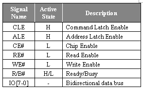
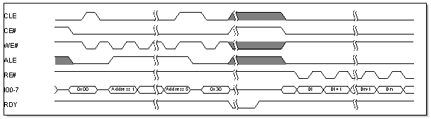
Figure 1. Page read operation on the asynchronous interface
Source synchronous interface
Source synchronous interface introduced in ONFI 2.0 standard is similar to DDR SRAM interface. There is a bidirectional strobe signal (DQS), the read and write signals has been combined into one signal. Data over data bus are transferred at both edges of the DQS signal, therefore with DQS running at 100MHz we can get 200MT/s (Megatransfers per second).
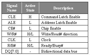
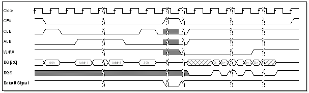
Figure 2. Page read operation on source synchronous interface
Commands
The NAND Flash memory is controlled using set of commands; set that vary from memory to memory. According to ONFI Standard (5) the below list is a basic mandatory command set with their respective command codes (first/second byte).
- Read, 00h/30h
- Change Read Column, 05h/E0h
- Block Erase, 60h/D0h
- Read Status, 70h
- Page Program, 80h/10h
- Change Write Column, 85h
- Read ID, 90h
- Read Parameter Page, ECh
- Reset, FFh
Internal architecture
As it was said in the beginning, the NAND Flash memory does not allow to randomly access any location in the memory. Instead, there are groups of bytes called pages to be requested. In case of read the requested page is internally transferred from flash matrix into the page register and only from there page data can be accessed in a serial-alike way byte by byte starting from the byte at indicated location within the page. The address within the active page can be freely changed to read other bytes from the given memory page. Changing page address requires to re-execute the matrix read command.
Pages are grouped into blocks which are the smallest area than can be erased, the single page is the smallest region that can be programmed. Blocks are organized in planes and planes in logic units (LUN).
Below diagram presents example architecture of the memory having the following parameters:
- Page size: 4320 B (4096B + 224B)
- Block size: 128 pages
- Plane size: 512 blocks
- LUN size: 4 planes
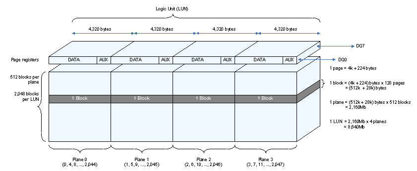
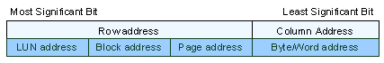
As mentioned above in the previous chapter, the address information is fed into the memory chip through an 8-bit interface; therefore, the address is divided into bytes. Currently the address sequence is up to 5 bytes (cycles) long, they are always ordered from the least to the most significant one. The address is divided into four logical parts that are correlated with the memory structure. The first two bytes represent byte location within the page, and it is called column address. The other three bytes contain page address, block address and LUN selection, which are collectively called row address. The column address always indicates a memory word location, not a single byte location. Therefore, for a 2KB-page having 2112 bytes per page, there are 2112 valid addresses for an 8-bit memory interface and 1056 addresses for a 16-bit memory interface. Consequently, for the same page size column address is shorter by one bit for memory with a 16-bit data interface.
It is also important to say that pages need to be written in consecutive order within the block, page number 0 is to be written first followed by page 1 write. Writing out of the sequence is not allowed, as violating this rule aggravates bit error rate. A single block does not need to be written all at once. That is, block can be written with pages from 0 to 11, and later on with pages from 12 to 32, for example. Generally, pages need to be written as a whole at once though some memories support so called ‘partial page programming’, which allows a subpage of 512 bytes + correlated spare area to be written (please see below). There is a limited number of partial writes allowed.
Page organization
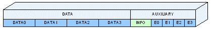
Pages are power of two kilobytes in size (2KB, 4KB, 8KB …) extended by some additional space. The basic area is called data area while the extended part can be called auxiliary or spare area. This spare area is dedicated to store error correction codes and metadata. The metadata contains management information like erase cycle counter, bad block mark, logical address information. These two spaces – data and auxiliary – have not been clearly distinguished in form of access, so the actual organization of the page is up to the designer. They can select whatever is more convenient for them. Additionally user data is divided into subpages, that is, codewords for separate ECC calculation. The most common way is to store data in lower part of the page and metadata along with error correction checksums in the upper part, as it has been depicted below.
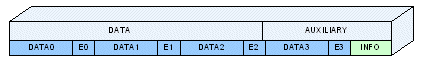
Some implementations prefer different organization to increase performance or usability. Below diagram depicts situation that error correction checksum is stored immediately after each subpage.
However, in many cases user does not need to care about page organization as dedicated controller or flash management software handles it for them.
Error source and type
The source of error could be overprogramming, program disturb, charge loss, charge leakage between neighboring cells or charge trap in floating gate oxide.
Not all of them are unrecoverable, therefore they have been divided into two groups - hard and soft errors. Hard errors are the ones that are non- recoverable; the charge trap belongs to them. The charge trap is responsible for wear-out of the memory cells over time and it appears at erase or program operation.
The other group, the soft errors can be fixed by block erase/reprogram cycle. They usually appear at read operation and could be invisible to the user as the ECC can correct them.
The memory use scheme influences the bit error rate. Partial-page programming, non-sequential pages programming within the block, excessive read per block without erase as well as non-equal number of read operation within a single block increase number of the read disturb errors. (2)
Error correction
To meet application bit error rate, that is, to become less vulnerable to and protected against errors the error correction is required. It is even more crucial while working with MLC type memories due to their inherent higher vulnerability to the charge loss. At the time when small SLC memories were prevalent on the market just simple Hamming algorithm was far enough. Its ability to correct single bit error and detection two bit error suited most systems and it could be even implemented in software. Nowadays with high density and MLC memories, more sophisticated algorithms started to be used on a much wider scale. Two which should be listed here are Reed-Salomon and BCH (Bose, Ray-Chaudhuri and Hocquenghem); the latter one is much more common, mostly due to better performance in terms of speed as well as silicon area. It is highly recommended to use hardware acceleration of the BCH algorithm.
Many memory controllers available off-the-shelf contain various ECC options including Hamming and BCH. Implementing ECC in hardware reduces processor load and allows to better optimize algorithm by increasing its performance as implementation of Galois field operations is impractical in software due to lack of hardware support for finite field multiplication (1). Hardware implementation supports also parallel processing of algorithm steps.
Bad block and wear-leveling
To increase production yield and to reduce manufacturing costs the NAND Flash memory is allowed to contain some limited number of bad blocks when shipped from factory. The bad block is block containing more bit errors that recommended ECC can correct. The bad blocks do not influence performance of the memory as blocks are isolated from each other.
According to the ONFI Standard bad block mark is to be located at the first address of the first or last page of bad block (5). Vendors that do not follow ONFI Standard may employ other bad mark location.
As the factory testing procedures are very rigorous and conducted in various conditions it is crucial to scan the whole memory and build initial bad-block table before any erase/program operation happens. The initial bad-block information should be carefully recorded and maintained because the number of bad blocks increases over use time.
The bad block information is usually stored in each memory block and in the dedicated system table. The system table stores the living copy of the bad-block table. In the event when the living copy is invalidated, it can be restored by reading bad block marks from all blocks in the memory. It is very important to keep all bad block marks up-to-date, valid and intact. Alternatively, the system can store a backup of the bad-block table and use it to restore the living copy.
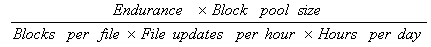
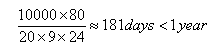
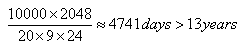
The erase/program cycles cause memory cells to gain some extra charge (trap electrons); accumulation of this charge over time leads to wear-out the memory cells. To alleviate this effect equalization of erase/write cycles number throughout the memory is required and is called wear-leveling. In this way, life of the memory can be significantly prolonged while reducing the increase of the bad-blocks. Just to illustrate (4), let’s assume having a NF memory of 2048 blocks in size with endurance of 10’000 erase/program cycles. System updates 3 files 20 blocks each, every file is updated 3 times per hour, so totally there are 9 updates per hour. The following equation (4) can be used to calculate the memory lifetime.
Without wear-leveling only 80 blocks are effectively used. Let’s calculate the lifetime for this case:
With wear-leveling, the whole memory is used, so 2048 blocks are reused - let’s calculate the lifetime of these 2048 blocks:
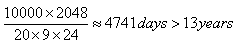
This simple calculations proves that wear-leveling is required and worth its effort to implement.
Software
To manage different aspects and characteristics of NAND Flash memory a dedicated software support is required. Below a short explanation of Flash Translation Layer, Bad block management, Wear-leveling and Garbage collection is presented.
FTL, bad-blocks management and wear-leveling
Flash Translation Layer is responsible for translating logical address of the sector into the physical address of memory page. It is required as flash requires erase-before-write approach and "does not like" excessive multiple writes into the same location. FTL is tightly coupled with bad block management and wear-leveling. As it has been explained earlier, bad block management assures that bad blocks are not used, so if access to the corrupted location is requested, it is relocated to the correct location.
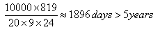
There are two wear-leveling management methods - static and dynamic. The basic difference is in the size of block pool. The dynamic wear leveling only equalizes blocks with dynamic data, that is, the blocks that store files which are frequently updated. Consequently, the managed block pool is just a part of the whole memory. Let’s assume that 60% of the memory from the previous example contains static data (such as operating system, media files, etc) and 40% stores dynamic data (logs, file usage counters, FAT table, etc.). This 40% translates into 819 blocks in the dynamic pool with the following lifetime:
The static wear-leveling optimizes the wear throughout the memory. Blocks storing dynamic as well as static data are managed, when the usage counter difference between blocks containing static and dynamic data reaches certain level then the data are swapped between blocks and the least wear blocks are used for storing dynamic data. Consequently, the theoretical lifetime is over 13 years.
This longer lifetime of the memory under dynamic wear is gain at the cost of higher software overhead. Other advantages and disadvantages of both methods have been presented in (4)
Garbage Collection
Garbage Collection is a process of cleaning the memory. As a result of writing and updating data within the memory, some pages become invalidated. This causes fragmentation of the memory over time. It is up to the Garbage Collection to select the appropriate block, moving all its valid pages to the new block and erasing the selected block. In this way free blocks become available for write operation.
Garbage collection is usually triggered by a low level of free blocks. It can also run as a periodic task or as a background operation of the operating system. Garbage collection assures that the system is not starved by a lack of free blocks for writing data. The importance of garbage collection increases with the escalation of data update operations.
File System
The file system exists on the top of the NAND Flash software pyramid. It provides mechanism for accessing files in easy and familiar fashion. File system can be dedicated for NAND Flash (JFFS2, SafeFLASH) and in such a case it integrates support for Flash management or it can be a more general purpose file system such as FAT16/32. In the latter case the dedicated flash management layer with FTL and Garbage Collection is required. Selection of file system is driven by many factors, which are beyond scope of this paper.
File system contains procedures for storing file location and assuring data integrity across the media. The user Application Programming Interface (API) is usually composed of a set of standard C functions such as fopen, fread, fwrite, ferase, fclose.
Building system – elements to consider as a summary
Building system with NAND Flash memory is not an easy and straightforward task. It requires analysis of many factors and conditions not only memory vendor and memory density, but also page and spare area size, interface and its performance, error correction algorithm and software. To optimize usage of the memory the connection scheme needs to be evaluated taking into account usage scenario that greatly influences system performance and level of complexity. (1)
Some solutions can work with just a single memory chip while others could require a whole matrix of chips formed into banks with multichip bus supporting interlaced operations. Utilizing multichip bus can increase throughput several times. To give just an overview, single-chip bus working with asynchronous interface and dedicated controller with Hamming ECC reaches 21 MB/s, the multi-chip bus for the same conditions (4x 8-bit chips) achieves 70 MB/s
Some systems may work with NAND Flash memory tied directly to microprocessor data bus, while others cannot work without a dedicated controller. It is especially applicable for high-speed memories with synchronous DDR interface. Controller offloads memory operation from the main microprocessor, it handles error correction, specific memory operation scheme and executes automatic transfers between system memory and NAND Flash chips. In more sophisticated solutions controller can optimize the memory operation sequence to achieve maximum performance. In many cases usage of relatively simple controller can significantly simplify the design and reduce microprocessor load.
Some controllers support also boot from NAND Flash, that is, some dedicated page(s) are loaded into RAM at system start-up. With this approach usage of dedicated program ROM can be avoided.
Software side of the solution is also very important part. Usually system utilizing NAND Flash memory employs some kind of file system (FAT16/32, JFFS2, SafeFLASH). In simpler, not file system demanding application, just a Flash Translation Layer could be enough.
Fail-safe
A very important subject that needs to be mentioned here is a fail-safe aspect of the NAND Flash application. If it is required to preserve stable state of the memory, then the fail-safe needs to be considered at every level of application from bottom to top from NAND Flash memory to user application (3). Such points like power stability, data write order and metadata stability information need to be taken into consideration.
Bibliography
1. LEILEI SONG, KESHAB K. PARHI, ICHIRO KURODA, AND TAKAO NISHITANI. Hardware/Software Codesign of Finite Field Datapath for Low-Energy Reed–Solomon Codecs. IEEE TRANSACTIONS ON VERY LARGE SCALE INTEGRATION (VLSI) SYSTEMS. April 2000, Vol. 8, No. 2, p. 160.
2. JIM COOKE, MICRON TECHNOLOGY, INC. Flash Memory Technology Direction. WinHEC, 2007
3. DAVE HUGHES. Designing fail-safe storage systems for embedded applications. Embedded Control Europe. September 2009, p. 6-7.
4. MICRON TECHNOLOGY, INC. Wear-leveling Techniques in NAND Flash Devices. Micron Technology, Inc. October 2008.
5. Open NAND Flash Interface Specification, Revision 2.2, October 7, 2009. www.onfi.org
6. MICRON TECHNOLOGY, INC. NAND Flash Design and Use Considerations. August 2008.
7. THOMAS COUGHLIN. Digital Storage in Consumer Electronics. Burlington, MA. Elsevier, Inc. 2008. ISBN-13: 978-0-7506-8465-1
本文来自博客园,作者:dolinux,未经同意,禁止转载

 浙公网安备 33010602011771号