
ARM Cortex-M0 MCU Design Learning | Part0
1. 简介
Cortex-M0 DesignStart 组件旨在用于基于 Cortex-M0 处理器的原型 SoC 的 SystemVerilog 设计与仿真。
项目资料地址:https://github.com/ForrestBlue/cortexm0ds
1.1 Cortex-M0 DesignStart 组件包含:
- An ARM Cortex-M0 processor from DesignStart.(处理器)
- An example system-level design for the ARM Cortex-M0 processor.(样例系统)
- Reusable AMBA components for system-level development.(AMBA 组件)
1.2 Cortex-M0 DesignStart 组件目录结构:

2. 系统级结构
2.1 System-level Design Hierarchy
Figure1 给出了该 MCU 的顶层结构框图。Table1 给出了各模块的简要描述以便理解系统构成。
Figure1. Top level view of cmsdk_mcu
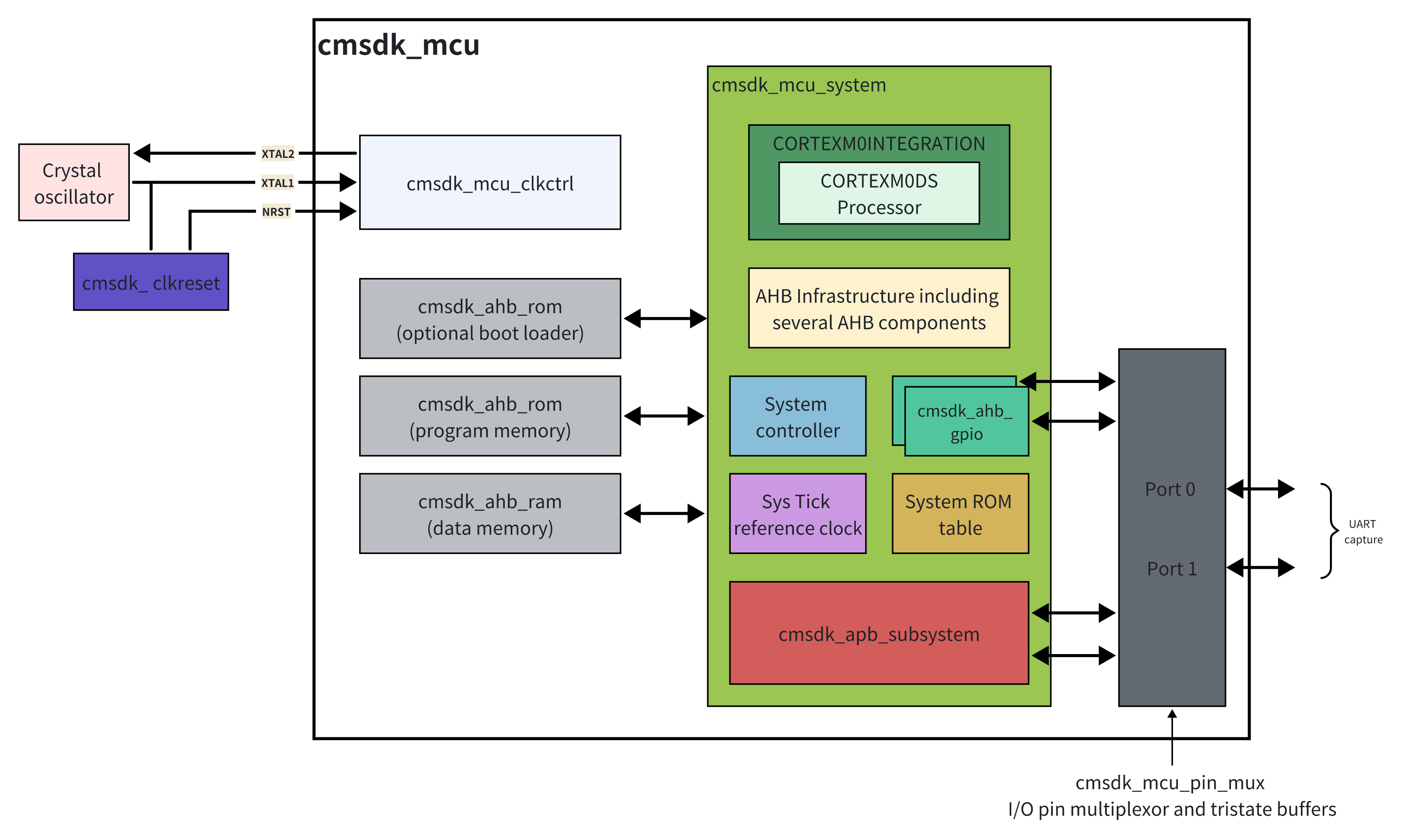
Table1. The component of cmsdk_mcu
| Item | Description |
|---|---|
| cmsdk_mcu | The example microcontroller design. This level contains the behavioral memories and clock generation components. |
| cmsdk_mcu_system | The synthesizable level of the microcontroller design. This instantiates the Cortex-MO processor. |
| CORTEXMOINTERGRATION | Instantiates the CORTEXM0DS layer. |
| CORTEXM0DS | The Cortex-M0 Integration layer. This is obfuscated code. |
| cmsdk_apb_subsystem | A subsystem of APB peripherals and APB infrastructure. |
| System controller | Contains programmable registers for system control, for example memory remap. |
| SysTick reference clock | SysTick reference clock generation logic. |
| cmsdk_ahb_gpio | A low-latency GPIO with an AHB interface. Each GPIO module provides 16 I/O pins. |
| cmsdk_mcu_clkctrl | The clock and reset generation logic behavioral model. ( CRU ) |
| cmsdk_mcu_pin_mux | The pin multiplexor and tristate buffers for the I/O ports. |
| cmsdk_ahb_rom | A memory wrapper for the ROM to test the behavior of different implementations of memory. You can modify the Verilog parameters to change the implementation. |
| cmsdk_ahb_ram | A memory wrapper for the RAM to test the behavior of different implementations of memory. You can modify the Verilog parameters to change the implementation. |
| cmsdk_ahb_cs_rom_table | An example system level CoreSight ROM table that enables a debugger to identify the system as a Corte-MO base system. |
| cmsdk_mcu_addr_decode | Generates the HSELS for each memory mapped component based on the CMSDK address map. |
2.2 Cortex-M0 example system
Figure 2 给出了基于 Cortex-M0 的一个系统例子。Table2 给出了组件的解释说明,便于理解。
用户可以通过多种不同的方式来配置系统。 该 Cortex-M0 处理器通过 AHB Lite 接口与系统的其他部分进行连接。
Figure2. Cortex-M0 example system

Table2. The peripheral components that system design includes.
| Item | Description |
|---|---|
| cmsdk_ahb_default_slave | AHB slave (default) |
| cmsdk_ahb_gpio | AHB gpio |
| cmsdk_ahb_to_iop | Simple AHB to IOP Bridge (for use with the IOP GPIO to make an AHB GPIO). |
| cmsdk_ahb_slave_mux | Simple AHB slave multiplexer (1 to 10) |
| cmsdk_ahb_to_apb | Simple AHB to APB bridge |
| cmsdk_apb_dualtimers | Timers module containing two 32-bit down-counters. |
| cmsdk_apb_slave_mux | APB slave multiplex (1 to 16) |
| cmsdk_apb_subsystem | APB sub system |
| cmsdk_apb_timer | Simple APB timer |
| cmsdk_apb_uart | Simple APB UART |
| cmsdk_apb_watchdog | APB watchdog timer |
| cmsdk_apb4_eg_slave | APB example slave, support AMBA APB4. slave is always ready and response is always OKAY. |
| cmsdk_iop_gpio | Simple IOP GPIO |
| cmsdk_clock_gate | Behavioral model of clock gating cell |
| cmsdk_ahb_ram_beh | Simple AHB RAM behavioral model |
| cmsdk_ahb_ram | Simple AHB RAM model wrapper |
| cmsdk_ahb_rom | Simple AHB ROM model wrapper |
3. 学习思路
首先从系统层面看,该 MCU 系统已经算是较为完整了,有 cpu 核,有各种外设(包含 AHB 和 APB Peripheral),呈现 CPU - AHB - APB 的结构,不尽人意的是没有更高速的 AXI 总线。应该是因为该处理器核是 AHB 的接口,所以是这样的结构。其实在实际芯片设计时,都是可以挂在 Subsys Noc 上的,所以学习价值还是有的;
其次,组件中除处理器核外还包含各类外设 IP,虽然是简单的行为级 IP,但对于 IP 的功能/行为逻辑的学习理解也是有价值的;
最后,后续将会以数字芯片设计的流程从 处理器核、外设IP、系统集成等方面展开学习总结,包含各 IP 和 系统级的 RTL 理解 ——> 编译 ——> 仿真验证 ——> Spyglass ——> DC。

 浙公网安备 33010602011771号