

ADI高速信号采集芯片与JESD204B接口简介
ADI高速信号采集芯片与JESD204B接口简介
JESD204B接口
介绍:
JEDEC Standard No. 204B (JESD204B)—A standardized serial interface between data converters (ADCs and DACs) and logic devices (FPGAs or ASICs)
也就是说这是一个高速模数信号转换芯片与逻辑器件芯片之间的标准接口。
JEDEC是开发微电子行业开放标准的全球领导者,拥有3,000多名志愿者,代表近300家成员公司。官网:https://www.jedec.org/
特点:
优点:具有所有高速串行接口的优点(减小芯片封装大小、引脚数量;减小电路板PCB面积;功率一定时提供更大的吞吐量。);
速度:每个Lane/通道高达12.5 Gbps(12.5 * 10 ^ 9 bits per second = 12.5 * 10 ^ 8 Bytes per second(8b/10b编码) ~= 1192.0929 MBytes per second(除以1024 ^ 2))。
子类:
JESD204B接口共有三个子类:Subclass 0 Subclass 1 Subclass 2(常见Subclass 1,不同子类的区别主要跟信号SYSREF和SYNC~的有无有关):
Subclass 0 uses device clock, lanes, and SYNC~(子类0只有SYNC~信号);
Subclass 1 uses device clock, lanes, SYNC~, and SYSREF(子类1有SYNC~和SYSREF信号);
Subclass 2 uses device clock, lanes, and SYNC~(子类2只有SYNC~信号)。
架构:
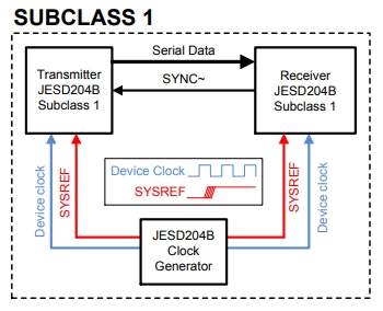
以上图片来自:http://www.ti.com/lit/ml/slap161/slap161.pdf
图中显示了一个基本的JESD204B(Subclass 1)的架构,时钟产生器给收发双方提供Device Clock及SYSREF信号;发送方通过串行接口发送数据至接收方,接收方通过SYNC~信号控制发送进程。
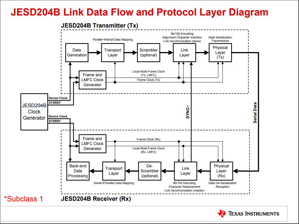
以上图片来自:http://www.ti.com/lit/ml/slap161/slap161.pdf
从图中我们可以看到:
架构分三层:1 Transport Layer / 传输层;2 Link Layer / 链路层;3 Physical Layer / 物理层。
比较重要的信号有Device Clock、SYSREF和SYNC~:
Device Clock提供外部统一同步时钟;
SYSREF由外部时钟产生器生成;
SYNC~由接收发给发送,用于同步。
deterministic link latency
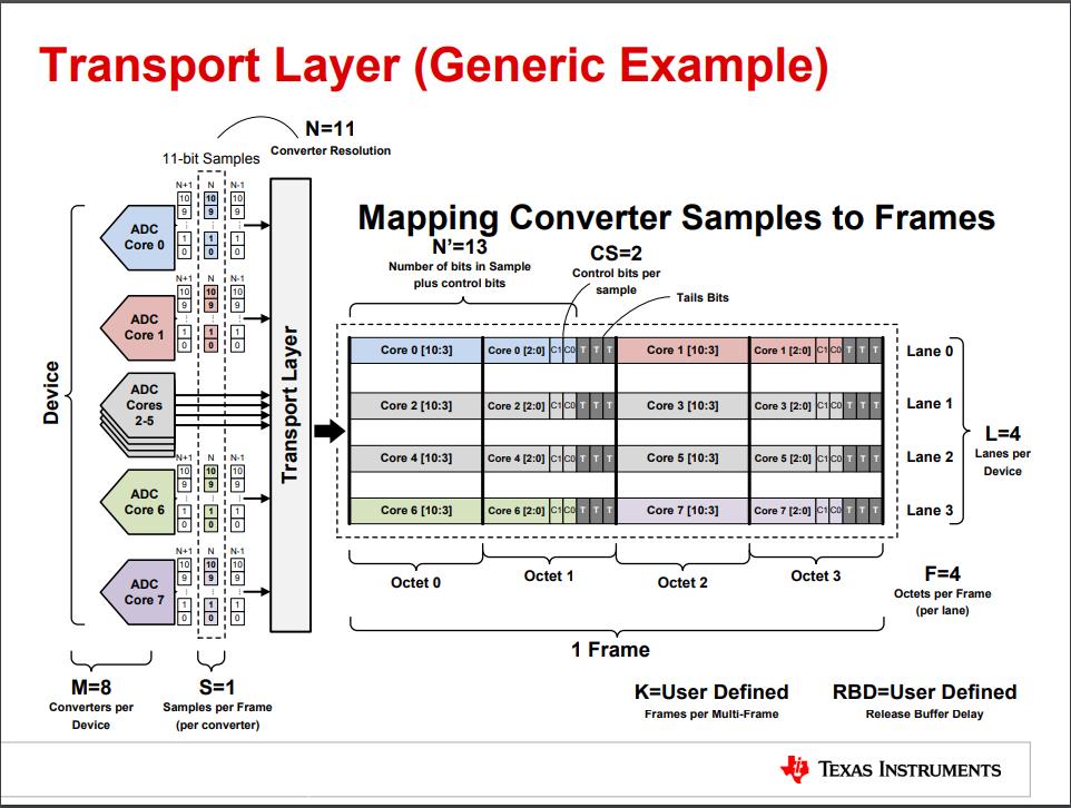
上图中各参数:
M=8表示共有8路ADC;S=1表示一帧中包含了1次采样;N=11表示ADC采样精度为11;N'=13表示采样精度11bits+控制位2bits;CS=2表示控制位为2bits;L=4表示Lane的数量为4;F=4表示每个Lane的每个帧有4个字节;K=User Defined表示由用户定义的每个多帧里面有几个帧;Control bits用于表示ADC是否溢出或;Tails Bits用于填充,可以固定为0或填充伪随机序列;
上述参数都是通过寄存器进行设置的。
初始化:
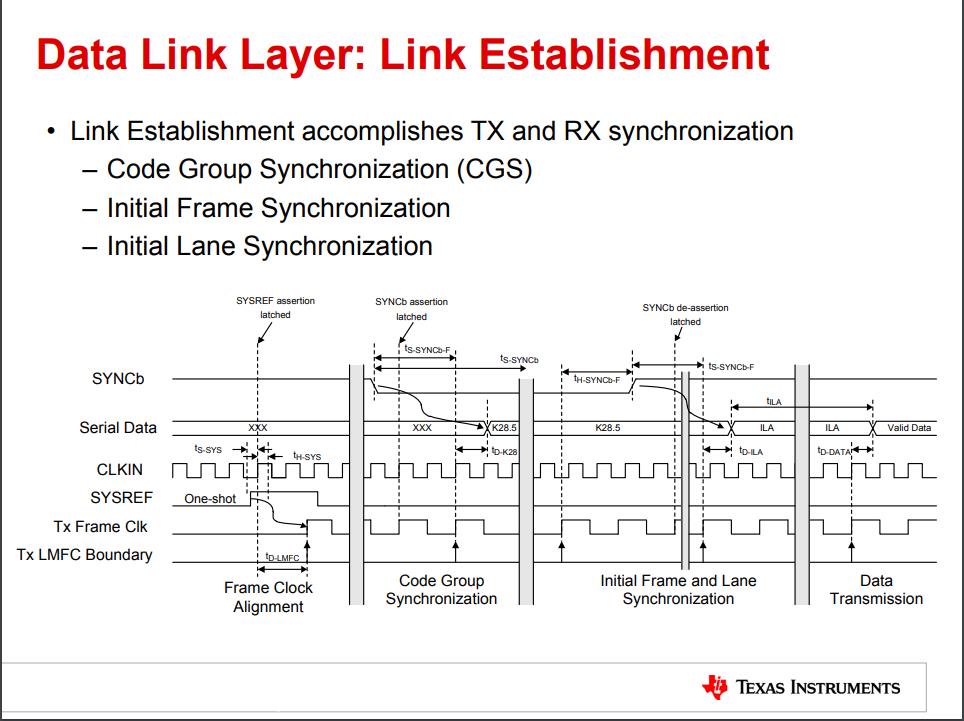
JESD204B通过三个阶段来建立同步链路:代码组同步(code group synchronization, CGS),初始化通道同步(initial lane synchronization, ILAS),数据传输阶段(data transmission phase)。
1.代码组同步(CGS)阶段
CGS is the process by which the JESD204B receiver finds the boundaries between the 10-bit symbols in the stream of data.
CGS阶段:
a 首先由接收端将SYNC信号拉低(表示请求与发送端同步);
b 发送端检测到SYNC信号拉低后,发送连续的K28.5字符;
c 接收端利用CDR(时钟数据恢复)技术,提取到四个连续的K28.5字符(表示同步完成)后,将SYNC拉高;
d 发送端检测到SYNC信号拉高后,即代表CGS阶段的完成,代码组同步阶段完成,进入ILAS阶段。
换个说法再来一遍:各接收器(FPGA)必须利用时钟和数据恢复(CDR)技术,在ADC传来的输入数据流中找到K28.5字符。一旦在所有链路通道上检测到某一数量的连续K28.5字符,接收器模块就会解除置位至发送器模块的SYNC~信号。在JESD204B中,发送模块捕捉SYNC~信号的变化,并在下一个本地多帧时钟(LMFC)边界上启动ILAS。
2.初始通道同步(ILAS)阶段
ILAS的主要作用是对齐链路的所有通道,验证链路参数,以及确定帧和多帧边界在接收器的输入数据流中的位置。
The ILAS phase follows the CGS phase and begins on the next LMFC boundary after SYNCINB± deassertion.
The ILAS consists of four mulitframes, with an /R/ character marking the beginning and an /A/ character marking the end.
ILAS包含4个多帧,由一个/R/码开始,由一个/A/码结束(/R/码为/K28.0/ /A/码为/K28.3/);
The ILAS begins by sending an /R/ character followed by 0 to 255 ramp data for one multiframe. On the second multiframe, the link configuration data is sent, starting with the third character. The second character is a /Q/ character to confirm that the link configuration data follows. All undefined data slots are filled with ramp data. The ILAS sequence is never scrambled.
The four multiframes include the following:
Multiframe 1 begins with an /R/ character (/K28.0/) and ends with an /A/ character (/K28.3/).
Multiframe 2 begins with an /R/ character followed by a /Q/ character (/K28.4/), followed by link configuration parameters over 14 configuration octets (see Table 31) and ends with an /A/ character. Many of the parameter valuesare of the value – 1 notation.
Multiframe 3 begins with an /R/ character (/K28.0/) and ends with an /A/ character (/K28.3/).
Multiframe 4 begins with an /R/ character (/K28.0/) and ends with an /A/ character (/K28.3/).
3.用户数据阶段
在这一阶段,用户数据根据发送器(ADC)中定义并转发到接收器(FPGA)的链路参数,以流形式从发送器传输到接收器。接收器模块处理并监视收到的数据有无错误,包括运行差异不正确(8B/10B错误)、不在表中(8B/10B错误)、意外控制字符、 ILAS不正确和通道间偏斜。如果接收器检测到了错误,将会通过SYNC~报告错误。
参考:
ADI AD9695;
TI JESD204B;

 浙公网安备 33010602011771号