day01- stm32F4时钟配置
1、stm32时钟配置在启动阶段就配置好了,从启动代码入口跳转到系统初始化代码处


; Reset handler
Reset_Handler    PROC
                 EXPORT  Reset_Handler             [WEAK]
        IMPORT  SystemInit
        IMPORT  __main

                 LDR     R0, =SystemInit   // 进行系统初始化
                 BLX     R0
                 LDR     R0, =__main       // 跳转到main函数中执行我们的程序
                 BX      R0
                 ENDP
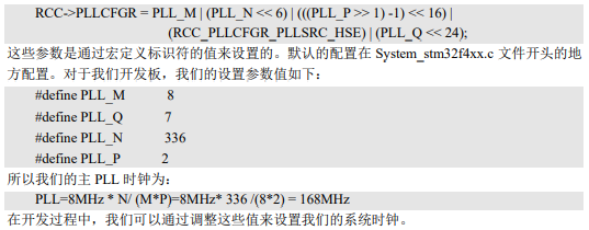
其中,systeminit进行浮点运算单元设置,然后是复位 PLLCFGR,CFGR 寄存器,同时 通过设置 CR 寄存器的 HSI 时钟使能位来打开 HSI 时钟。在这个函数中跳转到SetSysClock()函数中,进行HSE配置
/**
  * @brief  Setup the microcontroller system
  *         Initialize the Embedded Flash Interface, the PLL and update the
  *         SystemFrequency variable.
  * @param  None
  * @retval None
  */
void SystemInit(void)
{
  /* FPU settings ------------------------------------------------------------*/
  #if (__FPU_PRESENT == 1) && (__FPU_USED == 1)
    SCB->CPACR |= ((3UL << 10*2)|(3UL << 11*2));  /* set CP10 and CP11 Full Access */
  #endif
  /* Reset the RCC clock configuration to the default reset state ------------*/
  /* Set HSION bit    默认启用HSI时钟*/
  RCC->CR |= (uint32_t)0x00000001;

  /* Reset CFGR register */
  RCC->CFGR = 0x00000000;

  /* Reset HSEON, CSSON and PLLON bits */
  RCC->CR &= (uint32_t)0xFEF6FFFF;

  /* Reset PLLCFGR register */
  RCC->PLLCFGR = 0x24003010;

  /* Reset HSEBYP bit */
  RCC->CR &= (uint32_t)0xFFFBFFFF;

  /* Disable all interrupts */
  RCC->CIR = 0x00000000;

  /* Configure the System clock source, PLL Multiplier and Divider factors,
     AHB/APBx prescalers and Flash settings ----------------------------------*/
  SetSysClock();   // 在这里进行详细的HSE时钟配置,使用HSE时钟更精确

  /* Configure the Vector Table location add offset address ------------------*/
#ifdef VECT_TAB_SRAM
  SCB->VTOR = SRAM_BASE | VECT_TAB_OFFSET; /* Vector Table Relocation in Internal SRAM */
#else
  SCB->VTOR = FLASH_BASE | VECT_TAB_OFFSET; /* Vector Table Relocation in Internal FLASH */
#endif
}
其中,SetSysClock()先使能外部时钟 HSE,等待 HSE 稳定之后,配置 AHB,APB1,APB2 时钟相关的分频因子,也就是相关外设的时钟。等待这些都配置完成之后, 打开主 PLL 时钟,然后设置主 PLL 作为系统时钟 SYSCLK 时钟源。如果 HSE 不能达到就绪状 态(比如外部晶振不能稳定或者没有外部晶振),那么依然会是 HSI 作为系统时钟
/**
  * @brief  Configures the System clock source, PLL Multiplier and Divider factors,
  *         AHB/APBx prescalers and Flash settings
  * @Note   This function should be called only once the RCC clock configuration
  *         is reset to the default reset state (done in SystemInit() function).
  * @param  None
  * @retval None
  */
static void SetSysClock(void)
{
#if defined (STM32F40_41xxx) || defined (STM32F427_437xx) || defined (STM32F429_439xx) || defined (STM32F401xx)
/******************************************************************************/
/*            PLL (clocked by HSE) used as System clock source                */
/******************************************************************************/
  __IO uint32_t StartUpCounter = 0, HSEStatus = 0;

  /* Enable HSE */
  RCC->CR |= ((uint32_t)RCC_CR_HSEON);

  /* Wait till HSE is ready and if Time out is reached exit */
  do
  {
    HSEStatus = RCC->CR & RCC_CR_HSERDY;
    StartUpCounter++;
  } while((HSEStatus == 0) && (StartUpCounter != HSE_STARTUP_TIMEOUT));

  if ((RCC->CR & RCC_CR_HSERDY) != RESET)
  {
    HSEStatus = (uint32_t)0x01;
  }
  else
  {
    HSEStatus = (uint32_t)0x00;
  }

  if (HSEStatus == (uint32_t)0x01)
  {
    /* Select regulator voltage output Scale 1 mode */
    RCC->APB1ENR |= RCC_APB1ENR_PWREN;     // µçÔ´½Ó¿ÚʱÖÓʹÄÜ
    PWR->CR |= PWR_CR_VOS;    // Óë½ÚÄÜÏà¹Ø

    /* HCLK = SYSCLK / 1*/
    RCC->CFGR |= RCC_CFGR_HPRE_DIV1;

#if defined (STM32F40_41xxx) || defined (STM32F427_437xx) || defined (STM32F429_439xx)
    /* PCLK2 = HCLK / 2*/
    RCC->CFGR |= RCC_CFGR_PPRE2_DIV2;

    /* PCLK1 = HCLK / 4*/
    RCC->CFGR |= RCC_CFGR_PPRE1_DIV4;
#endif /* STM32F40_41xxx || STM32F427_437x || STM32F429_439xx */

    /* Configure the main PLL */
    RCC->PLLCFGR = PLL_M | (PLL_N << 6) | (((PLL_P >> 1) -1) << 16) |
                   (RCC_PLLCFGR_PLLSRC_HSE) | (PLL_Q << 24);

    /* Enable the main PLL */
    RCC->CR |= RCC_CR_PLLON;

    /* Wait till the main PLL is ready */
    while((RCC->CR & RCC_CR_PLLRDY) == 0)
    {
    }

#if defined (STM32F40_41xxx)
    /* Configure Flash prefetch, Instruction cache, Data cache and wait state */
    FLASH->ACR = FLASH_ACR_PRFTEN | FLASH_ACR_ICEN |FLASH_ACR_DCEN |FLASH_ACR_LATENCY_5WS;
#endif /* STM32F40_41xxx  */


    /* Select the main PLL as system clock source */
    RCC->CFGR &= (uint32_t)((uint32_t)~(RCC_CFGR_SW));
    RCC->CFGR |= RCC_CFGR_SW_PLL;

    /* Wait till the main PLL is used as system clock source */
    while ((RCC->CFGR & (uint32_t)RCC_CFGR_SWS ) != RCC_CFGR_SWS_PLL);
    {
    }
  }
  else
  { /* If HSE fails to start-up, the application will have wrong clock
         configuration. User can add here some code to deal with this error */
  }
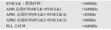
完成上面配置后,各总线时钟如下:
2、外设时钟的使能:所有的外设都挂在如下的5个总线下,其中APB1和APB2常用的外设总线
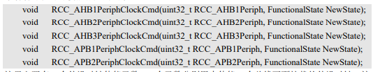
如果对于某个外设不清楚在那个总线下面,可以在stm32f4xx_rcc.h文件下查找。
3、中断分组:
在stm32中,中断具有两个属性:抢占属性、响应属性,属性的值越低,优先级越高;
抢占属性与响应属性使用4位来配置,因此可以有五种分配方式,就是5组:
0组:0级别抢占属性, 2^4级别响应属性;
1组:2^1级别抢占属性,2^3级别响应属性;
2组:2^2级别抢占属性,2^2级别响应属性;
3组:2^3级别抢占属性,2^1级别响应属性;
4组:2^4级别抢占属性,2^0级别响应属性;
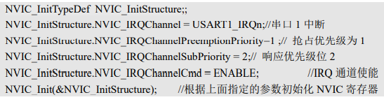
定义一个串口的中断优先级:
4、基于串口的printf函数实现

 浙公网安备 33010602011771号