【电路】差分接口互连(一)
对LVDS接口的研究
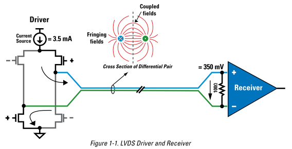
LVDS Output

VOS – Offset voltage: the common-mode voltage of the LVDS output。
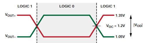
Output Common-Mode voltage 共模输出电压VOCM,在driver端叫做 offset voltage VOS,典型值是1.2V。
考虑到共模和差模电压的偏移,输出两端电压可以达到max 1.6V(1.375v + 450/2mv),min 0.9V(1.125v - 450/2mv)。
LVDS Input
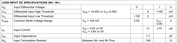
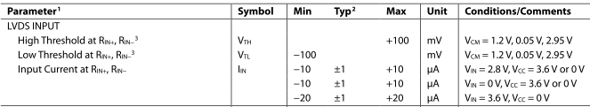
VCC is always higher than R IN+ and R IN− voltage. R IN− and R IN+ are allowed to have a voltage range of −0.2 V to VCC − VID/2.
However, to be compliant with ac specifications, the common voltage range is 0.1 V to 2.3 V.
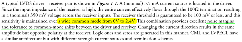
The ADN4662 differential line receiver is capable of receiving signals of 100 mV over a ±1 V common-mode range centered around 1.2 V.
This relates to the typical driver offset voltage value of 1.2 V. The signal originating from the driver is centered around 1.2 V and may shift ±1 V around this center point.
This ±1 V shifting may be caused by a difference in the ground potential of the driver and receiver, the common-mode effect of coupled noise, or both.
Wide input common mode range
设定芯片供电参数
输出接口要求

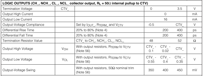
The board power supply (VTRM) is the voltage used to terminate the comparator outputs on the IC.
Setting VTRM to +1.2V makes the high-speed digital I/Os compatible with LVDS levels.
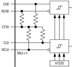
计算芯片输出接口的 Vocm = (CTV + CTV-400mv)/2 = CTV - 200mv;其必须符合后级
FPGA的输入共模范围Vicm = 0.3v~1.425v,即0.3v < Vocm < 1.425v,得出0.5V < CTV < 1.625V。
输入接口要求
The high-speed digital inputs (DATA0/NDATA0,RCV0/NRCV0, DATA1/NDATA1, and RCV1/NRCV1) are intended for use with a high-speed differential signal source such as LVDS, LVPECL, ECL, etc.
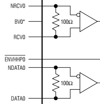


该片子内部有100欧姆终端电阻,非常适合匹配LVDS输出接口,而且单端电平及差分摆幅都很宽。
前级FPGA的标准LVDS Vocm = 1.25v,Vpp = 350m,得到1.075V < Vo < 1.425V;
手册标出最大Voh=1.675V,考虑到信号线与BV之间的esd管,则BV必须大于上面的值,BV>=1.675V,

取CTV=+1.625V,BV=+2.5V/+1.8V。
参考:
LVDS Owner's Manual Design Guide, 4th Edition
AN-1177: LVDS和M-LVDS电路实施指南 (Rev. 0)
SN65LVDS4、DS10BR150、ADN4661、ADN4662

 浙公网安备 33010602011771号