芯科BG22学习笔记:9-如何添加ADC(寄存器+图像化)
实验目的:BG22芯片添加ADC功能
实验环境:Simplicity Studio V5
实验器材:Wireless Starter Kit Mainboard (BRD4002A Rev B06) + EFR32xG22 2.4 GHz 6 dBm QFN40 Radio Board (BRD4182A)
实验开始:
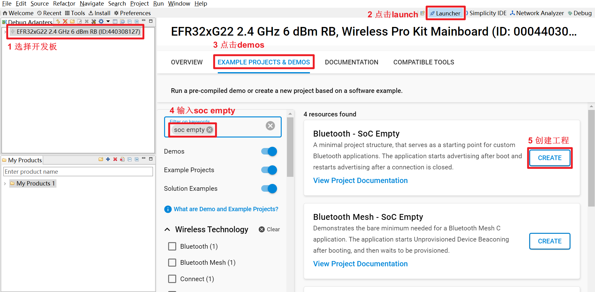
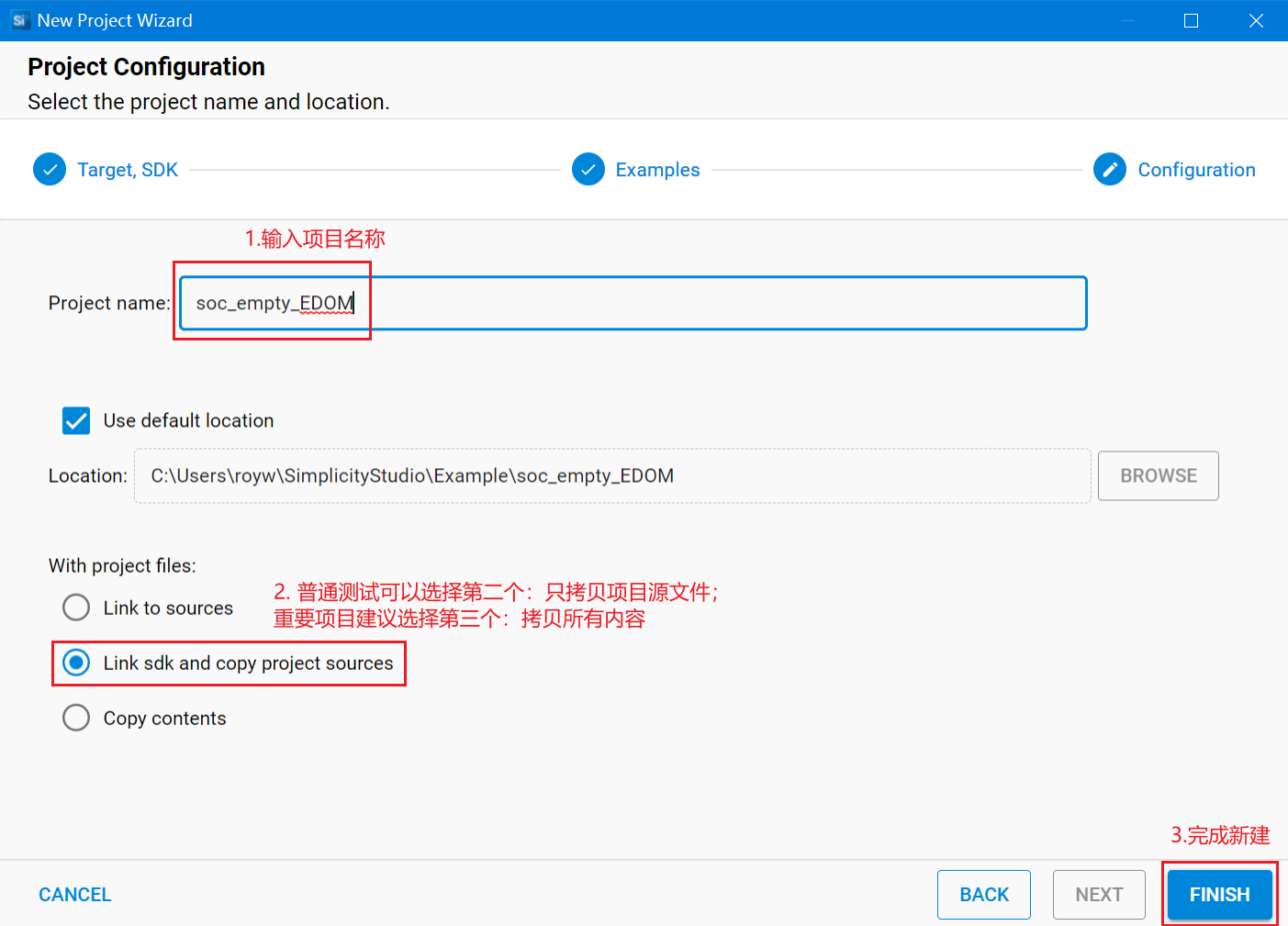
1. 新建工程,蓝牙工程输入soc empty, 普通MCU工程输入empty c
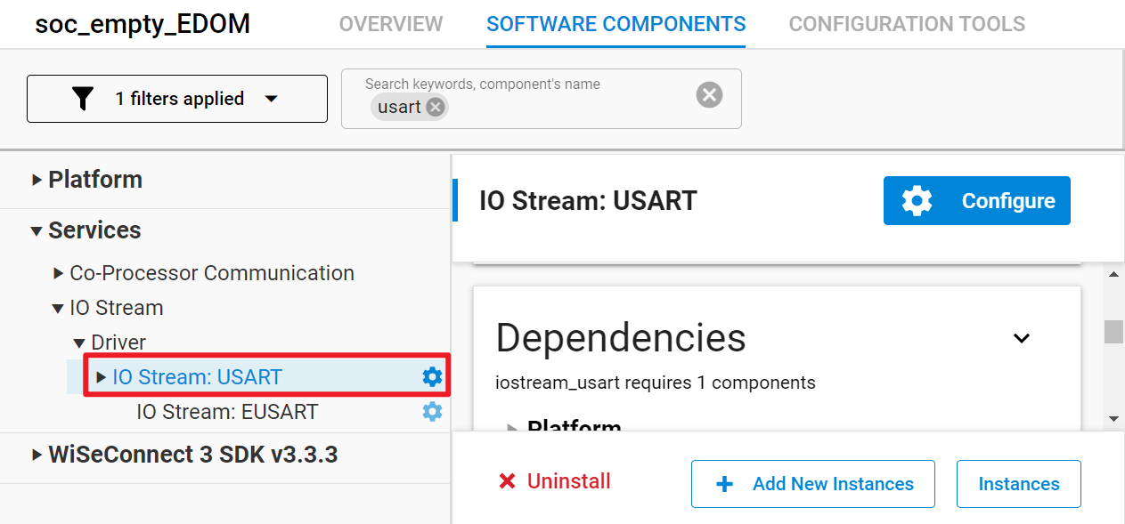
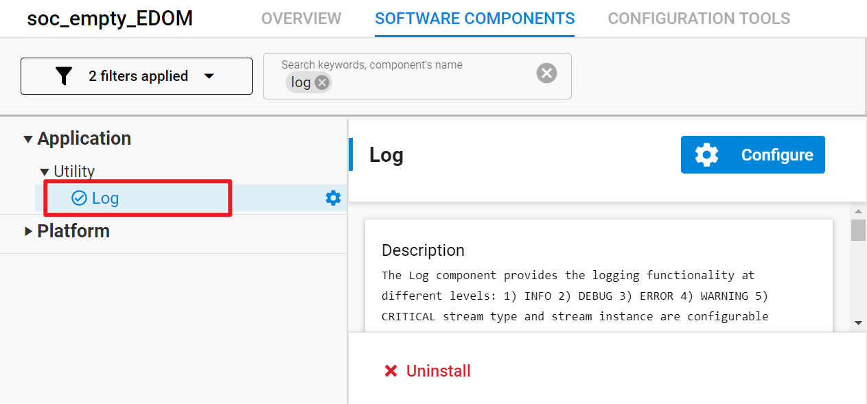
2. 添加组件:串口组件/LOG组件/浮点打印组件 (生成工程时系统已安装IADC组件,所以无需添加IADC组件)
3. app.c 替换成如下
#include "em_common.h"
#include "app_assert.h"
#include "sl_bluetooth.h"
#include "app.h"
#include "em_cmu.h"
#include "em_iadc.h"
#include "app_log.h"

// The advertising set handle allocated from Bluetooth stack.
static uint8_t advertising_set_handle = 0xff;

// Set CLK_ADC to 10MHz
#define CLK_SRC_ADC_FREQ      20000000  // CLK_SRC_ADC
#define CLK_ADC_FREQ          10000000  // CLK_ADC - 10 MHz max in normal mode

// Number of scan channels
#define NUM_INPUTS 8

/*
 * Specify the IADC input using the IADC_PosInput_t typedef.  This
 * must be paired with a corresponding macro definition that allocates
 * the corresponding ABUS to the IADC.  These are...
 *
 * GPIO->ABUSALLOC |= GPIO_ABUSALLOC_AEVEN0_ADC0
 * GPIO->ABUSALLOC |= GPIO_ABUSALLOC_AODD0_ADC0
 * GPIO->BBUSALLOC |= GPIO_BBUSALLOC_BEVEN0_ADC0
 * GPIO->BBUSALLOC |= GPIO_BBUSALLOC_BODD0_ADC0
 * GPIO->CDBUSALLOC |= GPIO_CDBUSALLOC_CDEVEN0_ADC0
 * GPIO->CDBUSALLOC |= GPIO_CDBUSALLOC_CDODD0_ADC0
 *
 * ...for port A, port B, and port C/D pins, even and odd, respectively.
 */
#define IADC_INPUT_0_PORT_PIN     iadcPosInputPortBPin0;
#define IADC_INPUT_1_PORT_PIN     iadcPosInputPortBPin1;

#define IADC_INPUT_0_BUS          BBUSALLOC                   //PB0是B BUS
#define IADC_INPUT_0_BUSALLOC     GPIO_BBUSALLOC_BEVEN0_ADC0  //PB0是B BUS的偶数管脚
#define IADC_INPUT_1_BUS          BBUSALLOC                   //PB1是B BUS
#define IADC_INPUT_1_BUSALLOC     GPIO_BBUSALLOC_BODD0_ADC0   //PB1是B BUS的奇数管脚

/*
 * This example enters EM2 in the main while() loop; Setting this #define
 * to 1 enables debug connectivity in EM2, which increases current
 * consumption by about 0.5 uA.
 */
#define EM2DEBUG                  1

/*******************************************************************************
 ***************************   GLOBAL VARIABLES   ******************************
 ******************************************************************************/

static volatile double scanResult[NUM_INPUTS];  // Volts

//#define IADC0_FIFOENTRIES 0x8UL in em_iadc.c
void initIADC (void)
{
  // Declare init structs
  IADC_Init_t init = IADC_INIT_DEFAULT;
  IADC_AllConfigs_t initAllConfigs = IADC_ALLCONFIGS_DEFAULT;
  IADC_InitScan_t initScan = IADC_INITSCAN_DEFAULT;
  IADC_ScanTable_t initScanTable = IADC_SCANTABLE_DEFAULT;    // Scan Table

  /*
   * Enable IADC0 and GPIO clock branches.
   *
   * Note: On EFR32xG21 devices, CMU_ClockEnable() calls have no effect
   * as clocks are enabled/disabled on-demand in response to peripheral
   * requests.  Deleting such lines is safe on xG21 devices and will
   * reduce provide a small reduction in code size.
   */
  CMU_ClockEnable(cmuClock_IADC0, true);
  CMU_ClockEnable(cmuClock_GPIO, true);

  // Select clock for IADC
  CMU_ClockSelectSet(cmuClock_IADCCLK, cmuSelect_FSRCO);

  // Modify init structures and initialize
  init.warmup = iadcWarmupKeepWarm;

  // Set the HFSCLK prescale value here
  init.srcClkPrescale = IADC_calcSrcClkPrescale(IADC0, CLK_SRC_ADC_FREQ, 0);

  /*
   * Configuration 0 is used by both scan and single conversions by
   * default.  Use internal bandgap as the reference and specify the
   * reference voltage in mV.
   *
   * Resolution is not configurable directly but is based on the
   * selected oversampling ratio (osrHighSpeed), which defaults to
   * 2x and generates 12-bit results.
   */
  initAllConfigs.configs[0].reference = iadcCfgReferenceInt1V2;
  initAllConfigs.configs[0].vRef = 1210;
  initAllConfigs.configs[0].osrHighSpeed = iadcCfgOsrHighSpeed2x;
  initAllConfigs.configs[0].analogGain = iadcCfgAnalogGain0P5x;

  // Divide CLK_SRC_ADC to set the CLK_ADC frequency
  initAllConfigs.configs[0].adcClkPrescale = IADC_calcAdcClkPrescale(IADC0,
                                             CLK_ADC_FREQ,
                                             0,
                                             iadcCfgModeNormal,
                                             init.srcClkPrescale);

  /*
   * Set the SCANFIFODVL flag when there are 4 entries in the scan
   * FIFO.  Note that in this example, the interrupt associated with
   * the SCANFIFODVL flag in the IADC_IF register is not used.
   *
   * Similarly, the fifoDmaWakeup member of the initScan structure
   * is left at its default setting of false, so LDMA service is not
   * requested when the FIFO holds the specified number of samples.
   */
  initScan.dataValidLevel = _IADC_SCANFIFOCFG_DVL_VALID4;

  // Tag FIFO entry with scan table entry id.
  initScan.showId = true;

  /*
   * Configure entries in scan table.  CH0 is single-ended from
   * input 0; CH1 is single-ended from input 1.
   */
  initScanTable.entries[0].posInput = IADC_INPUT_0_PORT_PIN;
  initScanTable.entries[0].negInput = iadcNegInputGnd;
  initScanTable.entries[0].includeInScan = true;

  initScanTable.entries[1].posInput = IADC_INPUT_1_PORT_PIN;
  initScanTable.entries[1].negInput = iadcNegInputGnd;
  initScanTable.entries[1].includeInScan = true;

  initScanTable.entries[2].posInput = iadcPosInputAvdd;      // Add AVDD to scan for demonstration purposes
  initScanTable.entries[2].negInput = iadcNegInputGnd | 1;   // When measuring a supply, PINNEG must be odd (1, 3, 5,...)
  initScanTable.entries[2].includeInScan = true;

  initScanTable.entries[3].posInput = iadcPosInputVddio;     // Add VDDIO to scan for demonstration purposes
  initScanTable.entries[3].negInput = iadcNegInputGnd | 1;   // When measuring a supply, PINNEG must be odd (1, 3, 5,...)
  initScanTable.entries[3].includeInScan = true;

  initScanTable.entries[4].posInput = iadcPosInputVss;       // Add VSS to scan for demonstration purposes
  initScanTable.entries[4].negInput = iadcNegInputGnd | 1;   // When measuring a supply, PINNEG must be odd (1, 3, 5,...)
  initScanTable.entries[4].includeInScan = false;            // FIFO is only 4 entries deep

  initScanTable.entries[5].posInput = iadcPosInputVssaux;    // Add VSSAUX (same as VSS) to scan for demonstration purposes
  initScanTable.entries[5].negInput = iadcNegInputGnd | 1;   // When measuring a supply, PINNEG must be odd (1, 3, 5,...)
  initScanTable.entries[5].includeInScan = false;

  initScanTable.entries[6].posInput = iadcPosInputDvdd;      // Add DVDD to scan for demonstration purposes
  initScanTable.entries[6].negInput = iadcNegInputGnd | 1;   // When measuring a supply, PINNEG must be odd (1, 3, 5,...)
  initScanTable.entries[6].includeInScan = false;

  initScanTable.entries[7].posInput = iadcPosInputDecouple;  // Add DECOUPLE to scan for demonstration purposes
  initScanTable.entries[7].negInput = iadcNegInputGnd | 1;   // When measuring a supply, PINNEG must be odd (1, 3, 5,...)
  initScanTable.entries[7].includeInScan = false;

  // Initialize IADC
  IADC_init(IADC0, &init, &initAllConfigs);

  // Initialize scan
  IADC_initScan(IADC0, &initScan, &initScanTable);

  // Allocate the analog bus for ADC0 inputs 对应GPIO管脚设置为模拟输入
  GPIO->IADC_INPUT_0_BUS |= IADC_INPUT_0_BUSALLOC;
  GPIO->IADC_INPUT_1_BUS |= IADC_INPUT_1_BUSALLOC;

  // Clear any previous interrupt flags
  IADC_clearInt(IADC0, _IADC_IF_MASK);

  // Enable Scan interrupts
  IADC_enableInt(IADC0, IADC_IEN_SCANTABLEDONE);

  // Enable ADC interrupts
  NVIC_ClearPendingIRQ(IADC_IRQn);
  NVIC_EnableIRQ(IADC_IRQn);
}


/**************************************************************************//**
 * @brief  IADC interrupt handler
 *****************************************************************************/
void IADC_IRQHandler(void)
{
  IADC_Result_t result = {0, 0};
  app_log_info("ADC IRQ Happened.\n");
  // While the FIFO count is non-zero...
  while (IADC_getScanFifoCnt(IADC0))
  {
    // Pull a scan result from the FIFO
    result = IADC_pullScanFifoResult(IADC0);

    /*
     * Calculate the voltage converted as follows:
     *
     * For single-ended conversions, the result can range from 0 to
     * +Vref, i.e., for Vref = VBGR = 1.21V, and with analog gain = 0.5
     * 0xFFF represents the full scale value of 2.42V.
     */
    scanResult[result.id] = result.data * 2.42 / 0xFFF;
  //  sl_app_log("ScanResult:%.2f\r\n", scanResult[result.id]);//打印输出数值
    /*
     * Scan results 2 - 6 are for external supply voltages, which are
     * presented to the IADC divided by 4 for conversion.  Back this
     * out to get the correct result in volts.  Note that DECOUPLE,
     * scan table entry 7 in this example, is an internal supply (the
     * output of the core supply regulator) and is connected directly
     * to the IADC without a divide-by-4 stage.
     */
    if ((result.id > 1) && (result.id < 7))
    {
      scanResult[result.id] *= 4;
    }
   // app_log_info("scanID: 0x%02x\n",  result.id);
    app_log_info("scanID: 0x%02x,scanResult: %.2fV\n", result.id, scanResult[result.id]);

  }

  // Alternate between the first and second set of scan table entries.
//  if (result.id == 3) {
//    IADC_setScanMask(IADC0, 0x00F0);
//  }
//  else {
//    IADC_setScanMask(IADC0, 0x000F);
//  }

  /*
   * Clear the scan table complete interrupt.  Reading FIFO results
   * does not do this automatically.
   */
  IADC_clearInt(IADC0, IADC_IF_SCANTABLEDONE);
}

/**************************************************************************//**
 * Application Init.
 *****************************************************************************/
SL_WEAK void app_init(void)
{
  /////////////////////////////////////////////////////////////////////////////
  // Put your additional application init code here!                         //
  // This is called once during start-up.                                    //
  /////////////////////////////////////////////////////////////////////////////
  app_log_init();
  initIADC();
  app_log_info("ADC initialed.\n");
#ifdef EM2DEBUG
#if (EM2DEBUG == 1)
  // Enable debug connectivity in EM2
  EMU->CTRL_SET = EMU_CTRL_EM2DBGEN;
#endif
#endif
}

/**************************************************************************//**
 * Application Process Action.
 *****************************************************************************/
SL_WEAK void app_process_action(void)
{
  /////////////////////////////////////////////////////////////////////////////
  // Put your additional application code here!                              //
  // This is called infinitely.                                              //
  // Do not call blocking functions from here!                               //
  /////////////////////////////////////////////////////////////////////////////

  //sl_app_log("START IADC.\r\n");
}

/**************************************************************************//**
 * Bluetooth stack event handler.
 * This overrides the dummy weak implementation.
 *
 * @param[in] evt Event coming from the Bluetooth stack.
 *****************************************************************************/
void sl_bt_on_event(sl_bt_msg_t *evt)
{
  sl_status_t sc;

  switch (SL_BT_MSG_ID(evt->header)) {
    // -------------------------------
    // This event indicates the device has started and the radio is ready.
    // Do not call any stack command before receiving this boot event!
    case sl_bt_evt_system_boot_id:
      // Create an advertising set.
      sc = sl_bt_advertiser_create_set(&advertising_set_handle);
      app_assert_status(sc);

      // Generate data for advertising
      sc = sl_bt_legacy_advertiser_generate_data(advertising_set_handle,
                                                 sl_bt_advertiser_general_discoverable);
      app_assert_status(sc);

      // Set advertising interval to 100ms.
      sc = sl_bt_advertiser_set_timing(
        advertising_set_handle,
        160, // min. adv. interval (milliseconds * 1.6)
        160, // max. adv. interval (milliseconds * 1.6)
        0,   // adv. duration
        0);  // max. num. adv. events
      app_assert_status(sc);
      // Start advertising and enable connections.
      sc = sl_bt_legacy_advertiser_start(advertising_set_handle,
                                         sl_bt_legacy_advertiser_connectable);
      app_assert_status(sc);
      break;

    // -------------------------------
    // This event indicates that a new connection was opened.
    case sl_bt_evt_connection_opened_id:

      IADC_command(IADC0, iadcCmdStartScan);
      IADC_setScanMask(IADC0, 0x00FF);
      break;

    // -------------------------------
    // This event indicates that a connection was closed.
    case sl_bt_evt_connection_closed_id:
      // Generate data for advertising
      sc = sl_bt_legacy_advertiser_generate_data(advertising_set_handle,
                                                 sl_bt_advertiser_general_discoverable);
      app_assert_status(sc);

      // Restart advertising after client has disconnected.
      sc = sl_bt_legacy_advertiser_start(advertising_set_handle,
                                         sl_bt_legacy_advertiser_connectable);
      app_assert_status(sc);
      break;

    ///////////////////////////////////////////////////////////////////////////
    // Add additional event handlers here as your application requires!      //
    ///////////////////////////////////////////////////////////////////////////

    // -------------------------------
    // Default event handler.
    default:
      break;
  }
}
4. 该程序每次连蓝牙成功后触发一次ADC转换;转换完成后进一次中断,从FIFO中读出4个数据(FIFO深度为4);其中前两个数据为PB00和PB01的电压值;
完

 浙公网安备 33010602011771号