AMD MPSoC PS PCIe Endpoint 使用要点
AMD MPSoC PS PCIe 使用要点
需求
有客户需要通过PCie从Windows系统访问MPSoC的DDR,从而使X86和A53通过共享DDR内存的方式交互大量数据。X86作为PCIe Host, MPSoC作为PCIe Endpoint。共享的DDR内存是MPSoC的DDR内存。
文档要点
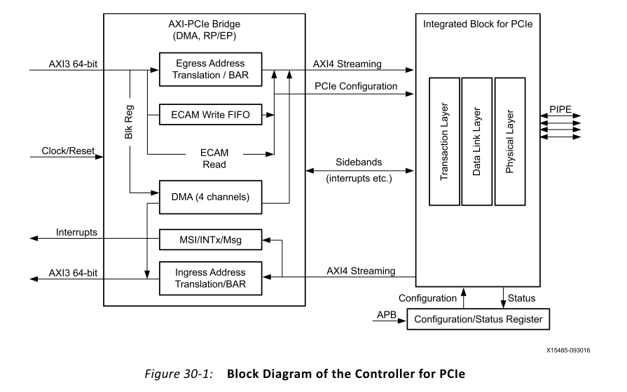
框图
首先,UG1085 Figure 30‐1: Block Diagram of the Controller for PCIe 提供了MPSoC PCIe部分的框图。从中可以看到,客户需要的是Ingress传输,即X86的PCIe请求达到MPSoC PCIe 控制器后,转换成AXI Master,再取读写MPSoC的DDR内存。
地址转换窗口
UG1085中的“Address Translation”部分,说明了MPSoC PCIe 控制器提供了8个地址转换的窗口。
Address Translation

The bridge provides eight fully-configurable address apertures to support address
translation both for ingress (from PCIe to AXI) and egress (from AXI to PCIe) transactions.
• In an AXI master, up to eight ingress translation regions can be set up. Translation is
done for the PCIe TLPs that are not decoded as MSI or MSI-X interrupts or internal
DMA transactions.
地址转换
如果PCIe地址的高位(基地址),等于source address (tran_src_base) 的高位,就会进行PCIe地址转换。
In the following discussions, the term tran refers to ingress/egress translation. For example,
tran_size refers to translation size and a tran_src_base refers to ingress/egress_src_base.

A translation is hit when the following occurs.
    • Translation is enabled (tran_enable == 1).
    • The tran_src_base[63:(12+tran_size)] == source address [63:(12+tran_size)].
转换后的目标地址,等于destination address (tran_dst_base)的高位(基地址),加上PCIe地址的低位(偏移地址)。
On a hit, the upper source address bits are replaced with destination base address bits
before forwarding the transaction to the destination.
    Destination address = {tran_dst_base[63:(12+tran_size)]  source address[12+tran_size]}.
地址转换窗口示例
1. Consider host assigns PCIe BAR2 = 0xFFA0_0000 ; 1MB size.
2. Ingress source base =  0xFFA0_0000 ; destination base =  0x44A0_0000 ;
aperture size = 64 KB
3. Incoming PCIe memory transaction hitting BAR2 at  0xFFA0_xyzw  translates to address
0x44A0_xyzw  on AXI master port.
示例代码
AMD提供了Standalone的示例"xilinxprocessoriplib\drivers\pciepsu\examples\Xpciepsu_ep_enable_example.c” 和 “xilinxprocessoriplib\drivers\pciepsu\src\Xpciepsu_ep.c”。
总体流程
"xilinxprocessoriplib\drivers\pciepsu\examples\Xpciepsu_ep_enable_example.c” 中的main()实现了总体流程,包括检查PCIe 链路状态,PCIe配置状态,最后再配置地址转换窗口。
int main()
{
	int Status = XST_SUCCESS;
#ifdef XPAR_PSU_PCIE_DEVICE_ID
	XPciePsu_InitEndPoint(&PciePsuInstance, XPAR_PSU_PCIE_DEVICE_ID);

	xil_printf("Waiting for PCIe Link up\r\n");
	XPciePsu_EP_WaitForLinkup(&PciePsuInstance);
	xil_printf("PCIe Link up...\r\n");

	XPciePsu_EP_BridgeInitialize(&PciePsuInstance);
	xil_printf("Bridge Init done...\r\n");

	XPciePsu_EP_WaitForEnumeration(&PciePsuInstance);

	xil_printf("Host driver indicated ready\r\n");
	int result = XPciePsu_EP_SetupIngress(&PciePsuInstance,
			INGRESS_NUM, BAR_NUM, PS_DDR_ADDR);
	if (result == XST_FAILURE) {
		xil_printf("PCIE ingress setup failed\r\n");
	} else {
		xil_printf("PCIE Ingress Test done\r\n");
	}

#endif
	return Status;
}
下面的参数定义了地址转换窗口数量、PCIe BAR、MPSoC的DDR内存的基地址。可以根据需要修改。
BAR_NUM定义了PCIe BAR的序号,在PCIe Host上一定要使用对应的BAR中的地址来访问。
#define INGRESS_NUM	0x0		/* Ingress num to setup ingress */
#define BAR_NUM		0x2		/* Bar no to setup ingress */
#define PS_DDR_ADDR	0x1000000	/* 32 or 64 bit PS DDR Addr
地址转换配置代码
XPciePsu_EP_SetupIngress()从PCIe BAR中读到PCIe的基地址,写入INGRESS0_SRC_BASE(tran_src_base, TRAN_INGRESS_SRC_BASE)。
接下来,XPciePsu_EP_SetupIngress()把MPSoC的DDR内存的基地址写入INGRESS0_DST_BASE(tran_dst_base, TRAN_INGRESS_DST_BASE)。
最后,XPciePsu_EP_SetupIngress() 设置 INGRESS0_CONTROL(TRAN_INGRESS_CONTROL)的大小和使能位,使能地址转换。
在这之后,PCIe Host就能读写MPSoC的在地址范围[PS_DDR_ADDR, PS_DDR_ADDR+INGRESS_SIZE_ENCODING]内的DDR内存。
int XPciePsu_EP_SetupIngress(XPciePsu *PciePsuPtr, u32 IngressNum, u32 BarNum,
		u64 Dst){
	Xil_AssertNonvoid(PciePsuPtr != NULL);
	u32 SrcLo;
	u32 SrcHi;
	u32 Val;
	u32 DestLo;
	u32 DestHi;
	if (IngressNum > 7) {
		return XST_FAILURE;
	}

	XPciePSU_ReadBar(PciePsuPtr, BarNum, &SrcLo, &SrcHi);

	/*
	 * Using Ingress Address Translation 0 to setup translation
	 * to PS DDR
	 */
	XPciePsu_WriteReg(PciePsuPtr->Config.BrigReg,
			(INGRESS0_SRC_BASE_LO + (IngressNum * INGRESS_SIZE)),
			SrcLo & ~0xf);
	XPciePsu_WriteReg(PciePsuPtr->Config.BrigReg,
			(INGRESS0_SRC_BASE_HI +
			(IngressNum * INGRESS_SIZE)), SrcHi);

	XPciePsu_Dbg("Done writing the Ingress Src registers\r\n");

	DestLo = XPCIEPSU_LOWER32BITS(Dst);
	DestHi = XPCIEPSU_UPPER32BITS(Dst);
	XPciePsu_WriteReg(PciePsuPtr->Config.BrigReg,
			(INGRESS0_DST_BASE_LO +
			(IngressNum * INGRESS_SIZE)), DestLo);
	XPciePsu_WriteReg(PciePsuPtr->Config.BrigReg,
			(INGRESS0_DST_BASE_HI +
			(IngressNum * INGRESS_SIZE)), DestHi);

	XPciePsu_Dbg("Done writing the Ingress Dst registers\r\n");

	Val = XPciePsu_ReadReg(PciePsuPtr->Config.BrigReg, INGRESS0_CONTROL);

	XPciePsu_Dbg("Read Ingress Control register\r\n");

	Val &= (u32)(~INGRESS_SIZE_MASK);
	Val |= (((u32)INGRESS_SIZE_ENCODING << INGRESS_SIZE_SHIFT) |
		(u32)INGRESS_ENABLE | (u32)INGRESS_SECURITY_ENABLE);
	Val |= INGRESS_RD_WR_ATTR;
	XPciePsu_WriteReg(PciePsuPtr->Config.BrigReg,
			(INGRESS0_CONTROL + (IngressNum * INGRESS_SIZE)), Val);

	XPciePsu_Dbg("Done setting up the ingress trasnslation registers\r\n");
	return XST_SUCCESS;
}
注意事项
在PCIe Host和A53通过共享DDR内存的方式交互数据时,要注意cache管理。
对于A53写、PCIe Host读的数据,A53要做cache Flush操作,PCIe Host要做cache Invalidate操作。
对于PCIe Host写、A53读的数据,PCIe Host要做cache Flush操作,A53要做cache Invalidate操作。
另外,在UG1085、UG1087里,同一个寄存器的名称,可能有出入。比如UG1085里的tran_dst_base,对应UG1087的TRAN_INGRESS_SRC_BASE_LO和TRAN_INGRESS_SRC_BASE_HI。
参考文档
UG1085 Zynq UltraScale+ Device TRM (v2.2) December 4, 2020
Zynq UltraScale+ Devices Register Reference](https://www.xilinx.com/htmldocs/registers/ug1087/ug1087-zynq-ultrascale-registers.html)

 浙公网安备 33010602011771号