

MEMORY
半导体器件:
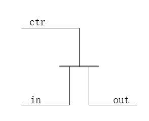
门电路:
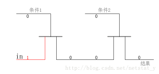
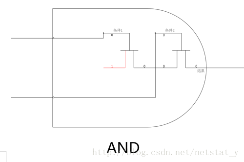
与:
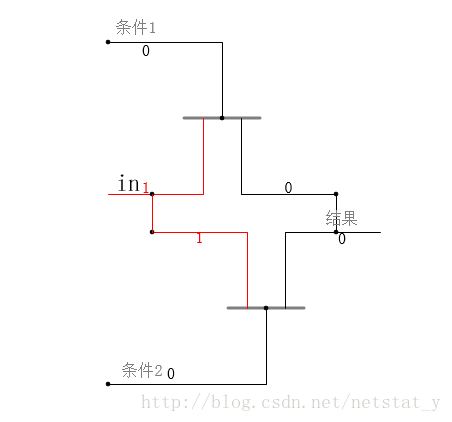
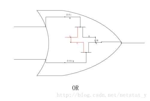
或:
非:
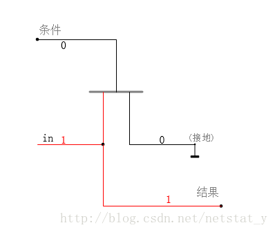

从上图的表示来看,我们可以把输入信号(待处理)看作是控制信号,主要功能是控制电流的通断。显而易见,它能结合电路(circuit)的串联、并联关系,关系清楚明了(至少是从整体上)。
图片来源:https://blog.csdn.net/netstat_y/article/details/79464244
以下文章来源于谷歌:
Memory Array Architectures
A SRAM Cell consists basically of 2 cross coupled CMOS inverters. By applying a logical 1 to the Wordline the internal values become visible at the Bitlines . The Bitline will have the value of the cell while the Bitline will have the complementary value. The reason is that if there is noise, the noise will influence both lines but will not change the voltage difference. Thats not the only reason, when writing a SRAM Cell we just can write a 0 and dependent on which side we do we set the value, this is due to the Vt drop at the wordline transistores. There are a lot more things to consider when dealing with SRAM Cells but as we are discussing the array architecture here I will skip this.

SRAM-Cell
1bit数据基本存储单元(SRAM)
A sense amplifier will have both bitlines as input and will return a single bit which is representing the value stored in the cell. Memory arrays are organized as row and columns (like a table). Rows are accessed using the Wordline, Columns are accessed by selecting a Bitline. In order to select a row or column we need address encoders.

SRAM Architecture
(以1bit为单位提取或存储数据的架构,行与列锁定位置)
As you can see we have 3 bits(000-111) for column addressing and 3 bits for row addressing. With 6 bits we can address SRAM-Cells (Bits). As you can see the SRAM architecture has a big transistor count, therefore it requires a lot of chip area and it also draws more power than eg. DRAM. But it is very fast and therefore used as Cache on the CPU of PCs. Also microcontrollers use SRAM as they usually do not have external RAM. The user is not interested in the internal architecture of the memory and also the user does not want to care about rows and columns. We simply define that the first 3 bits of the address define the row whereas the last 3 bits define the column. If we do so we end up with a table like this:
111000 111001 111010 111011 111100 111101 111110 111111
110000 110001 110010 110011 110100 110101 110110 110111
101000 101001 101010 101011 101100 101101 101110 101111
100000 100001 100010 100011 100100 100101 100110 100111
011000 011001 011010 011011 011100 011101 011110 011111
010000 010001 010010 010011 010100 010101 010110 010111
001000 001001 001010 001011 001100 001101 001110 001111
000000 000001 000010 000011 000100 000101 000110 000111
Memory Architectures with multi bit elements
We are usually not interested in addressing single bits, dependent on the surrounding architecture the size of a single memory elements is usually 8/32/64 bit.
There are different ways on how to implement the Address Decoder. I want to discuss 2 possibilities here, the combinatorial and the 1 hot (MUX) approach.
(我们一般以8bit为单位记录数据)
Combinatorial Address Decoder
We can simply check if the current address on the bus is ours using a big end gate,
The AND Gate above would activate the memory element if the address is 01100101.
(用一个有8个输入引脚的与门,锁定每一个存储单元--太麻烦)
To keep the schematic simple I illustrated a memory array with 4 address bits and therefore 16 memory elements. Every memory element gets the complete address and need to decide if it is addressed or not. For big arrays this causes a big overhead and also comes with the drawback that every memory element needs another address decoder

combinatorial addressing unidirectional datalines memory array
1 hot addressing
To overcome the issues with the combinatorial address encoding we can implement the 1 hot addressing which you already have seen with the SRAM Architecture. There are 2 address busses, one for the column and one for the row. Each of those busses has the same width as the original address and just one bit of each bus is allowed to be high at a time which means that we need to additional logic in order to generate those values but do not need complex address encoding inside the memory element as a simple AND gate is enough and all memory elements are now identical.

1 hot addressing unidirectional datalines memory array
(行与列的使用)
Bidirectional data lines
In the example above we had dedicated lines for input and output. Those lines can be combined to a bidirectional data bus. We need to make sure that we can switch the memory elements from read to write operation, therefore we need to introduce a switchable non inverting transmission gate(三态门,实现读写功能)
Additional we need to tell each memory element if it is in read or write state which requires additional wires.

combinatorial addressing bidirectional datalines memory array
DRAM:
dynamic RAM, is made of capacitors and must be refreshed every 10-100ms. It’s slower and cheaper than SRAM.
SRAM:
Static RAM, has a six transistor circuit in each cell and retains data, until powered off.
NVRAM:
Non-volatile RAM, retains its data, even when turned off. Example: Flash memory.


 浙公网安备 33010602011771号