

STM32F103 SPI 与W25Q64BV norFlash 驱动
STM32F103 SPI 与W25Q64BV norFlash 驱动
SPI,是英语Serial Peripheral interface的缩写,顾名思义就是串行外围设备接口。是Motorola首先在其MC68HCXX系列处理器上定义的。SPI接口主要应用在 EEPROM,FLASH,实时时钟,AD转换器,还有数字信号处理器和数字信号解码器之间。SPI,是一种高速的,全双工,同步的通信总线,并且在芯片的管脚上只占用四根线,节约了芯片的管脚,同时为PCB的布局上节省空间,提供方便,正是出于这种简单易用的特性,现在越来越多的芯片集成了这种通信协议。
SPI 具有信号线少,协议简单,数据率高等优点。数据传送速率达几MB/s
Pin 脚介绍
标准的 SPI 使用 4 Pin 进行数据传送:
(1)MOSI – 主器设备数据输出,从器件数据输入
(2)MISO – 主器设备件数据输入,从器件数据输出
(3)SCLK – 时钟信号,由主器件产生, 最大为fPCLK/2,从模式频率最大为fCPU/2
(4)NSS – 从器件使能信号,由主器件控制,有的 IC 会标注为 CS (Chip select)
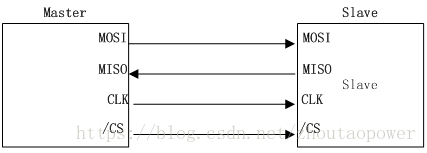
数据时在 CLK 时钟的驱动下,在数据线上按照一个 bit 一个 bit 的进行传送,数据可以在时钟的上升沿或者下降沿改变(或者采样)。
SPI 传输的缺点是,没有数据完整性校验,也没有流控机制。
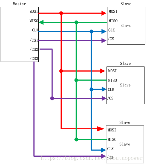
既然称 SPI 为总线,则 SPI 就可以支持多个设备相连接,通过 CS 片选信号来指定期望通讯的设备。(多机通讯)
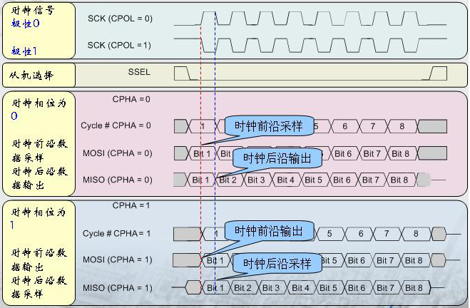
SPI 模式
SPI 通讯有 4 中不同的通讯模式,通信双方需要配置成为一样的模式,才能够进行正常的数据传输,这里有两个概念:
CPOL:时钟极性
CPHA:时钟相位
CPOL:(时钟极性)控制在没有数据传输时,SPI 时钟的空闲状态电平。即,定义了总线空闲的工作状态(注意,和 UART 不同,SPI 是通过 CLK 的状态来表征当前的总线状态,即不发生任何数据交互的时候,时钟信号总是没有进行翻转的)
CPOL=0,表示当SCLK=0时处于空闲态
CPOL=1,表示当SCLK=1时处于空闲态
CPHA:(时钟相位)是用来配置数据采样是在第几个边沿。
CPHA=0,表示数据采样是在第1个边沿
CPHA=1,表示数据采样是在第2个边沿
所以 CPOL 和 CPHA 的不同组合,成为了 SPI 的四种传输模式:
Mode Defination | CPOL Value | CPHA Value |
Mode0 | 0 | 0 |
Mode1 | 0 | 1 |
Mode2 | 1 | 0 |
Mode3 | 1 | 1 |
SPI Mode
四种传输模式,定义了不同时刻的总线启动,以及数据发送和采样时间:
CPOL=0,CPHA=0:此时空闲态时,SCLK处于低电平,数据采样是在第1个边沿,也就是 SCLK 由低电平到高电平的跳变,所以数据采样是在上升沿,数据发送是在下降沿。
CPOL=0,CPHA=1:此时空闲态时,SCLK处于低电平,数据发送是在第1个边沿,也就是 SCLK 由低电平到高电平的跳变,所以数据采样是在下降沿,数据发送是在上升沿。
CPOL=1,CPHA=0:此时空闲态时,SCLK处于高电平,数据采集是在第1个边沿,也就是 SCLK 由高电平到低电平的跳变,所以数据采集是在下降沿,数据发送是在上升沿。
CPOL=1,CPHA=1:此时空闲态时,SCLK处于高电平,数据发送是在第1个边沿,也就是 SCLK 由高电平到低电平的跳变,所以数据采集是在上升沿,数据发送是在下降沿。
对应到波形上:
STM32 SPI 特性
STM32 上支持 3 路 SPI:
- 可以支持全双工的通信
- 支持硬件 CRC
- 可编程的数据顺序,MSB在前或LSB在前
- 主模式和从模式的快速通信
- 可编程的时钟极性和相位(CPOL,CPHA)
- 可触发中断的专用发送和接收标志
- 可触发中断的主模式故障、过载以及CRC错误标志
- 支持DMA功能的1字节发送和接收缓冲器:产生发送和接受请求
SPI 时钟
单板上使用 SPI2 进行 SPI FLASH 的操作,使用的是 APB1 的时钟,最大配置为 36MHz。
硬件连接
硬件上,通过单板的 SPI2 引脚,连接到外部的 SPI FLASH (W25Q64)
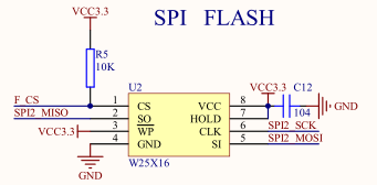
所以,在配置的时候,需要针对 SPI2 进行配置。
SPI Flash 简介
硬件单板上,连接的是 WinBond 的 W25Q64BV 的 SPI Flash,此款 Flash 的特性如下:
- 大小:64M-bit / 8M-byte
- 页 : 256B
- 支持 80MHz 的时钟
- 支持扇区擦除:Sector Erase (4K-bytes)
- 支持块擦除:Block Erase (32K and 64K-bytes)
- 支持页写入:0~256-bytes
- 软件/硬件写保护
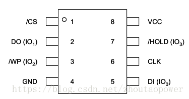
由于暂时不需要硬件写保护和Hold功能,故,直接将 WP和HOLD引脚接到 VCC(3.3V)
(此款SPI FLASH 还支持双线和4线 QSPI 的读写,由于 STM32 不支持,所以不在多说)
根据 W25Q64BV 的 Datasheet 描述,在操作这块 FLASH 的时候,需要配置主机为:
- SPI Mode 0 或者 Mode 3
- MSB 先传输
故,在 SPI2 配置的时候,需要进行对应的配置,才能够继续正常数据通信。
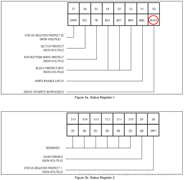
W25Q64BV 存在两个寄存器可以被访问,为 Status Register-1 和 Status Register-2,其中描述的关于 Write-Protect 的部分,暂时不管。与读写相关的就是 BUSY 位了,因为对 SPI Flash 编程后,Flash 需要内部的 cylce 进行数据的写入,内部program的时候会将 BUSY 置成 1,写入完成后,会将 BUSY 位置 0,故,每次对 Flash 进行写(包括擦除)之前,均要进行 BUSY 位的判断。
好啦,现在就开始按照 DateSheet 进行配置我们的 STM32 了。
STM32 SPI2 配置
配置过程主要分为两步:GPIO 的配置,SPI2 的配置(如原理图所示,PB_12 的 GPIO 用于了 CS 片选,我们需要将其配置成为输出的 GPIO,拉低的时候,选中 Flash,拉高的时候释放 Flash 信号)
1. 开启 GPIO B 组的时钟
2. 开启 SPI2 的时钟
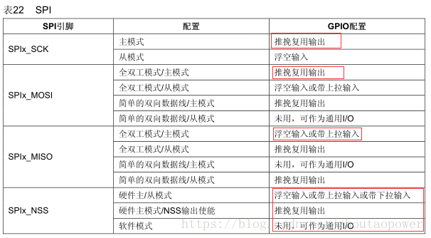
3. 按照 STM32 手册,配置 SCK 、MOSI 和 NSS 为复用推挽输出、MISO为浮空输入(有的代码将 MISO 配置成为的输出,虽然也可以运行,不过,您不觉得别扭么?还是遵循 Spec 的来吧)。同时将 GPIO_B _12配置为输出(CS信号)
4. 配置 SPI2 为全双工模式
5. SPI2 为 Master
6. SPI2 运行在 MODE3(按照 W25Q64BV 的 Timing 要求 )
7. SPI2 NSS 为软件模式(根本没用)
8. 预分频系数为 4 分频(APB1 为 36M,则 SPI2 的 SCK 为 9 MHz)
9. SPI2 传输 MSB(按照 W25Q64BV 的 Timing 要求)
10. 不启用 CRC
11. 开启 SPI 功能
此刻 SPI 的配置就基本完成了。接下来就是 按照 W25Q64BV 的 Timing 要求,写 FLASH 驱动咯.....
- #define SK_SPI_FLASH_CS_HIGH() GPIO_SetBits(GPIOB, GPIO_Pin_12)
- #define SK_SPI_FLASH_CS_LOW() GPIO_ResetBits(GPIOB, GPIO_Pin_12)
- /*******************************************************************************
- * Function Name : SK_SPIPortInit
- * Description : Configure the I/O port for SPI2.
- * Input : None
- * Output : None
- * Return : None
- *******************************************************************************/
- static void _SK_SPI2PortInit(void)
- {
- GPIO_InitTypeDef stGpioInit;
- /*!< Configure pins: SCK */
- stGpioInit.GPIO_Pin = GPIO_Pin_13;
- stGpioInit.GPIO_Speed = GPIO_Speed_50MHz;
- stGpioInit.GPIO_Mode = GPIO_Mode_AF_PP;
- GPIO_Init(GPIOB, &stGpioInit);
- /*!< Configure pins: MISO */
- stGpioInit.GPIO_Pin = GPIO_Pin_14;
- stGpioInit.GPIO_Mode = GPIO_Mode_IN_FLOATING;
- GPIO_Init(GPIOB, &stGpioInit);
- /*!< Configure pins: MOSI */
- stGpioInit.GPIO_Pin = GPIO_Pin_15;
- stGpioInit.GPIO_Speed = GPIO_Speed_50MHz;
- stGpioInit.GPIO_Mode = GPIO_Mode_AF_PP;
- GPIO_Init(GPIOB, &stGpioInit);
- /*!< Configure pins: CS */
- stGpioInit.GPIO_Pin = GPIO_Pin_12;
- stGpioInit.GPIO_Speed = GPIO_Speed_50MHz;
- stGpioInit.GPIO_Mode = GPIO_Mode_Out_PP;
- GPIO_Init(GPIOB, &stGpioInit);
- }
- /*******************************************************************************
- * Function Name : _SK_SPI2BusInit
- * Description : Configure the SPI2 Bus to adpte the W25Q64 Flash.
- * Input : None
- * Output : None
- * Return : None
- *******************************************************************************/
- static void _SK_SPI2BusInit(void)
- {
- SPI_InitTypeDef SPI_InitStructure;
- SPI_InitStructure.SPI_Direction = SPI_Direction_2Lines_FullDuplex;
- SPI_InitStructure.SPI_Mode = SPI_Mode_Master;
- SPI_InitStructure.SPI_DataSize = SPI_DataSize_8b;
- SPI_InitStructure.SPI_CPOL = SPI_CPOL_High;
- SPI_InitStructure.SPI_CPHA = SPI_CPHA_2Edge;
- SPI_InitStructure.SPI_NSS = SPI_NSS_Soft;
- SPI_InitStructure.SPI_BaudRatePrescaler = SPI_BaudRatePrescaler_4; // PCLK = 36M, SPI2 CLK = PCLK/4 = 9M
- SPI_InitStructure.SPI_FirstBit = SPI_FirstBit_MSB;
- SPI_InitStructure.SPI_CRCPolynomial = 7;
- SPI_Init(SPI2, &SPI_InitStructure);
- SPI_Cmd(SPI2, ENABLE);
- }
- /*******************************************************************************
- * Function Name : SK_SPIInit
- * Description : Initializes the peripherals used by the SPI FLASH driver.
- * Input : None
- * Output : None
- * Return : None
- *******************************************************************************/
- void SK_SPIFlashInit(void)
- {
- RCC_APB2PeriphClockCmd(RCC_APB2Periph_GPIOB, ENABLE);
- RCC_APB1PeriphClockCmd(RCC_APB1Periph_SPI2, ENABLE);
- _SK_SPI2PortInit();
- SK_SPI_FLASH_CS_HIGH();
- _SK_SPI2BusInit();
- }
W25Q64BV Flash 驱动
W25Q64BV 是 Flash 嘛,最主要的就是读和写。当然,除了这些,还有擦除功能,读 ID 等等。不着急,一步一步来,都是套路。
STM32 在进行 SPI 全双工数据传输的时候,在通过 MOSI 写出去数据后,可以立马进行 MISO 数据读取,通过轮询 TXE 标志来判断数据已经全部加载到移位寄存器,通过轮询 RXE 标志来得知本次 MISO 的数据已经全部到账。
针对 W25Q64BV Flash,Datasheet 中列出了支持的多种不同的命令:
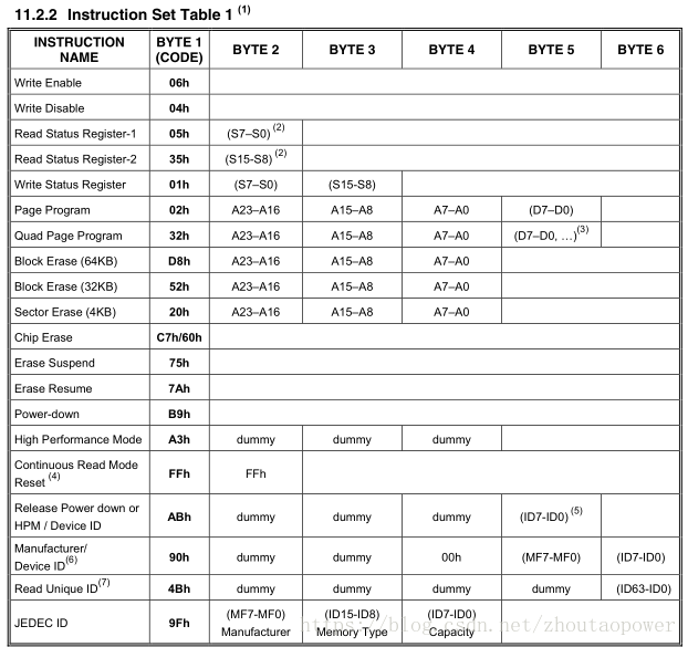
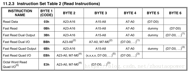
对应上述表格,有不同的 Timing 进行描述,比如:Opcode 为 0x9F 的时候,是读取一个叫 JEDEC ID 的东西:
可以看到,主机首先将 CS 拉低,然后主机处在 Mode 0 或者 Mode 3 的时候,在 MOSI 信号上输出 0x9F 的数据(命令),然后接着写入 Dummy Data (随便写点东西),然后再 MISO 信号上就能够收到 manufacture ID 的信息(为 0xEF),在继续写入 Dummy Data,继续接收,继续写入,继续接收,这样便可以得到期望的数据了。
获取 Flash ID 信息
根据上述方式,便可以获取 ID 信息:
- /********************** W25Q64 Flash Command Defination ***********************/
- #define SPI_FLASH_PerWritePageSize 256
- #define W25X_WriteEnable 0x06
- #define W25X_WriteDisable 0x04
- #define W25X_ReadStatusReg_1 0x05
- #define W25X_ReadStatusReg_2 0x35
- #define W25X_WriteStatusReg 0x01
- #define W25X_ReadData 0x03
- #define W25X_FastReadData 0x0B
- #define W25X_FastReadDual 0x3B
- #define W25X_PageProgram 0x02
- #define W25X_64K_BlockErase 0xD8
- #define W25X_32K_BlockErase 0x52
- #define W25X_4K_SectorErase 0x20
- #define W25X_ChipErase 0xC7
- #define W25X_PowerDown 0xB9
- #define W25X_ReleasePowerDown 0xAB
- #define W25X_DeviceID 0xAB
- #define W25X_ManufactDeviceID 0x90
- #define W25X_JedecDeviceID 0x9F
- #define Busy_Flag 0x01 /* Write In Progress (WIP) flag */
- #define Dummy_Byte 0xFF /* Dummy Data */
- typedef struct {
- uint8_t manufacturer_id;
- uint8_t memory_type_id;
- uint8_t capacity_id;
- uint8_t device_id;
- } W25Q64_ID_t;
- /*******************************************************************************
- * Function Name : SPI_FLASH_SendByte
- * Description : Sends a byte through the SPI interface and return the byte
- * received from the SPI bus.
- * Input : byte : byte to send.
- * Output : None
- * Return : The value of the received byte.
- *******************************************************************************/
- static uint8_t SPI_FLASH_SendByte(uint8_t byte)
- {
- /* Loop while DR register in not emplty */
- while (SPI_I2S_GetFlagStatus(SPI2, SPI_I2S_FLAG_TXE) == RESET);
- /* Send byte through the SPI2 peripheral */
- SPI_I2S_SendData(SPI2, byte);
- /* Wait to receive a byte */
- while (SPI_I2S_GetFlagStatus(SPI2, SPI_I2S_FLAG_RXNE) == RESET);
- /* Return the byte read from the SPI bus */
- return SPI_I2S_ReceiveData(SPI2);
- }
- /*******************************************************************************
- * Function Name : SK_GetFlashID
- * Description : Reads FLASH identification.
- * Input : W25Q64_ID_t pointer
- * Output : None
- * Return : FLASH identification
- *******************************************************************************/
- void SK_GetFlashID(W25Q64_ID_t *stW25Q64_ID)
- {
- SK_SPI_FLASH_CS_LOW();
- SPI_FLASH_SendByte(W25X_JedecDeviceID);
- stW25Q64_ID->manufacturer_id = SPI_FLASH_SendByte(Dummy_Byte);
- stW25Q64_ID->memory_type_id = SPI_FLASH_SendByte(Dummy_Byte);
- stW25Q64_ID->capacity_id = SPI_FLASH_SendByte(Dummy_Byte);
- SK_SPI_FLASH_CS_HIGH();
- }
- /*******************************************************************************
- * Function Name : SK_GetFlashDeviceID
- * Description : Reads FLASH Device identification.
- * Input : W25Q64_ID_t pointer
- * Output : None
- * Return : FLASH identification
- *******************************************************************************/
- void SK_GetFlashDeviceID(W25Q64_ID_t *stW25Q64_ID)
- {
- SK_SPI_FLASH_CS_LOW();
- SPI_FLASH_SendByte(W25X_DeviceID);
- SPI_FLASH_SendByte(Dummy_Byte);
- SPI_FLASH_SendByte(Dummy_Byte);
- SPI_FLASH_SendByte(Dummy_Byte);
- stW25Q64_ID->device_id = SPI_FLASH_SendByte(Dummy_Byte);
- SK_SPI_FLASH_CS_HIGH();
- }
擦除 Flash
Flash 的擦除分为三种,Sector 擦除(4K 为单位),Block擦除(32K or 64K 为单位)以及 Chip 擦除(全部擦除)
基本的方式都是一样的,支持命令不一样而已:
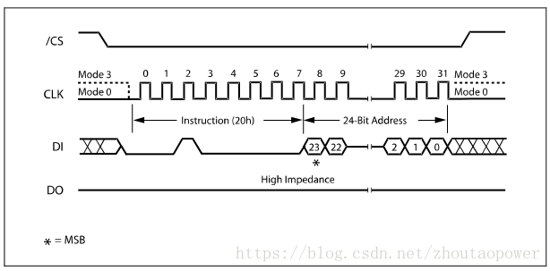
先拉低 CS,然后传输擦除的命令(0x20 or 0xD8 or 0x52),在传输期望擦除的地址起始值:24 bits Address,进行操作后,需要等待 BUSY 为 0 ,方可退出。
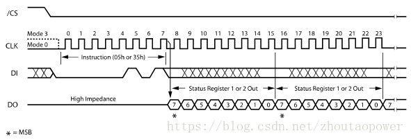
针对 BUSY 位的判断,是通过读取 Status Register-1 的最后一位来确定的:
- /*******************************************************************************
- * Function Name : SK_SPI_FLASH_WaitBusy
- * Description : Polls the status of the Write In Progress (WIP) flag in the
- * FLASH's status register and loop until write opertaion
- * has completed.
- * Input : None
- * Output : None
- * Return : None
- *******************************************************************************/
- void SK_SPI_FLASH_WaitBusy(void)
- {
- u8 FLASH_Status = 0;
- /* Select the FLASH: Chip Select low */
- SK_SPI_FLASH_CS_LOW();
- /* Send "Read Status Register" instruction */
- SPI_FLASH_SendByte(W25X_ReadStatusReg_1);
- /* Loop as long as the memory is busy with a write cycle */
- do
- {
- /* Send a dummy byte to generate the clock needed by the FLASH
- and put the value of the status register in FLASH_Status variable */
- FLASH_Status = SPI_FLASH_SendByte(Dummy_Byte);
- }
- while ((FLASH_Status & Busy_Flag) == SET); /* Write in progress */
- /* Deselect the FLASH: Chip Select high */
- SK_SPI_FLASH_CS_HIGH();
- }
- /*******************************************************************************
- * Function Name : SK_SPI_FLASH_Erase
- * Description : Erases the specified FLASH
- * Input : SectorAddr: address of the sector to erase.
- * Input : EraseType : The type of erase.
- * : W25X_4K_SectorErase (4KB Erase)
- * : W25X_32K_BlockErase (32KB Erase)
- * : W25X_64K_BlockErase (64KB Erase)
- * Output : None
- * Return : None
- *******************************************************************************/
- void SK_SPI_FLASH_Erase(uint32_t SectorAddr, uint8_t EraseType)
- {
- /* Send write enable instruction */
- SK_SPI_FLASH_WriteEnable();
- SK_SPI_FLASH_WaitBusy();
- /* Sector Erase */
- /* Select the FLASH: Chip Select low */
- SK_SPI_FLASH_CS_LOW();
- /* Send Sector Erase instruction */
- SPI_FLASH_SendByte(EraseType);
- /* Send SectorAddr high nibble address byte */
- SPI_FLASH_SendByte((SectorAddr & 0xFF0000) >> 16);
- /* Send SectorAddr medium nibble address byte */
- SPI_FLASH_SendByte((SectorAddr & 0xFF00) >> 8);
- /* Send SectorAddr low nibble address byte */
- SPI_FLASH_SendByte(SectorAddr & 0xFF);
- /* Deselect the FLASH: Chip Select high */
- SK_SPI_FLASH_CS_HIGH();
- /* Wait the end of Flash writing */
- SK_SPI_FLASH_WaitBusy();
- }
写 Flash
注意,在写 W25Q64BV Flash 的时候,Datesheet 规定,需要先写入 Write Enable 命令:
- /*******************************************************************************
- * Function Name : SK_SPI_FLASH_WriteEnable
- * Description : Enables the write access to the FLASH.
- * Input : None
- * Output : None
- * Return : None
- *******************************************************************************/
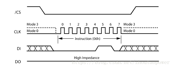
- void SK_SPI_FLASH_WriteEnable(void)
- {
- /* Select the FLASH: Chip Select low */
- SK_SPI_FLASH_CS_LOW();
- /* Send "Write Enable" instruction */
- SPI_FLASH_SendByte(W25X_WriteEnable);
- /* Deselect the FLASH: Chip Select high */
- SK_SPI_FLASH_CS_HIGH();
- }
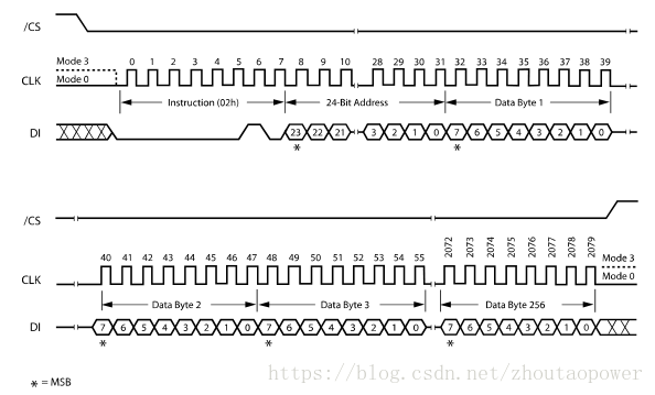
此刻代表 SPI Flash 已经处在可被写的状态,然后对 SPI FLASH 的写操作,支持 0~256-bytes的写操作:
当然,写完同样需要 Check Buys 位:
- /*******************************************************************************
- * Function Name : SK_SPI_FLASH_PageWrite
- * Description : Writes more than one byte to the FLASH with a single WRITE
- * cycle(Page WRITE sequence). The number of byte can't exceed
- * the FLASH page size.
- * Input : - pBuffer : pointer to the buffer containing the data to be
- * written to the FLASH.
- * - WriteAddr : FLASH's internal address to write to.
- * - NumByteToWrite : number of bytes to write to the FLASH,
- * must be equal or less than "SPI_FLASH_PageSize" value.
- * Output : None
- * Return : None
- *******************************************************************************/
- void SK_SPI_FLASH_PageWrite(uint8_t *pBuffer, uint32_t WriteAddr, uint32_t NumByteToWrite)
- {
- /* Enable the write access to the FLASH */
- SK_SPI_FLASH_WriteEnable();
- /* Select the FLASH: Chip Select low */
- SK_SPI_FLASH_CS_LOW();
- /* Send "Write to Memory " instruction */
- SPI_FLASH_SendByte(W25X_PageProgram);
- /* Send WriteAddr high nibble address byte to write to */
- SPI_FLASH_SendByte((WriteAddr & 0xFF0000) >> 16);
- /* Send WriteAddr medium nibble address byte to write to */
- SPI_FLASH_SendByte((WriteAddr & 0xFF00) >> 8);
- /* Send WriteAddr low nibble address byte to write to */
- SPI_FLASH_SendByte(WriteAddr & 0xFF);
- if(NumByteToWrite > SPI_FLASH_PerWritePageSize)
- {
- NumByteToWrite = SPI_FLASH_PerWritePageSize;
- }
- /* while there is data to be written on the FLASH */
- while (NumByteToWrite--)
- {
- /* Send the current byte */
- SPI_FLASH_SendByte(*pBuffer);
- /* Point on the next byte to be written */
- pBuffer++;
- }
- /* Deselect the FLASH: Chip Select high */
- SK_SPI_FLASH_CS_HIGH();
- /* Wait the end of Flash writing */
- SK_SPI_FLASH_WaitBusy();
- }
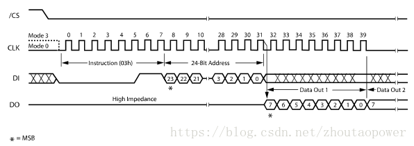
读 Flash
读数据的过程,同样也是先 CS 拉低,在写入读数据的指令(0x03),接着跟 24-bit 的地址信息。然后一直发送 Dummy Data,同时读到指定的数据到 BUFFER
- /*******************************************************************************
- * Function Name : SK_SPI_FLASH_BufferRead
- * Description : Reads a block of data from the FLASH.
- * Input : - pBuffer : pointer to the buffer that receives the data read
- * from the FLASH.
- * - ReadAddr : FLASH's internal address to read from.
- * - NumByteToRead : number of bytes to read from the FLASH.
- * Output : None
- * Return : None
- *******************************************************************************/
- void SK_SPI_FLASH_BufferRead(uint8_t* pBuffer, uint32_t ReadAddr, uint32_t NumByteToRead)
- {
- /* Select the FLASH: Chip Select low */
- SK_SPI_FLASH_CS_LOW();
- /* Send "Read from Memory " instruction */
- SPI_FLASH_SendByte(W25X_ReadData);
- /* Send ReadAddr high nibble address byte to read from */
- SPI_FLASH_SendByte((ReadAddr & 0xFF0000) >> 16);
- /* Send ReadAddr medium nibble address byte to read from */
- SPI_FLASH_SendByte((ReadAddr& 0xFF00) >> 8);
- /* Send ReadAddr low nibble address byte to read from */
- SPI_FLASH_SendByte(ReadAddr & 0xFF);
- while (NumByteToRead--)
- {
- *pBuffer = SPI_FLASH_SendByte(Dummy_Byte);
- pBuffer++;
- }
- /* Deselect the FLASH: Chip Select high */
- SK_SPI_FLASH_CS_HIGH();
- }
测试方式
在 main 函数中,初始化 SPI 后,进行 Flash 的 ID 读取,扇区擦除,数据读写的操作,同时,也可以进行数据写入后,断电,然后再次读出的操作,看看数据是否正确保存。
- #define SPI_FLASH_DATA_LEN 100
- #define SPI_FLASH_START_ADDR 0x00
- W25Q64_ID_t g_stW25Q64_ID;
- uint8_t g_spi_flash_rd_data[SPI_FLASH_DATA_LEN] = {0};
- uint8_t g_spi_flash_wr_data[SPI_FLASH_DATA_LEN] = {0};
- int main(void)
- {
- uint32_t i = 0;
- /* SPI FLASH TEST */
- SK_SPIFlashInit();
- SK_GetFlashID(&g_stW25Q64_ID);
- SK_GetFlashDeviceID(&g_stW25Q64_ID);
- SK_SPI_FLASH_Erase(SPI_FLASH_START_ADDR, W25X_4K_SectorErase);
- SK_SPI_FLASH_BufferRead(g_spi_flash_rd_data, SPI_FLASH_START_ADDR, SPI_FLASH_DATA_LEN);
- for (i = 0; i < SPI_FLASH_DATA_LEN; i++)
- g_spi_flash_wr_data[i] = i;
- SK_SPI_FLASH_PageWrite(g_spi_flash_wr_data, SPI_FLASH_START_ADDR, SPI_FLASH_DATA_LEN);
- SK_SPI_FLASH_BufferRead(g_spi_flash_rd_data, SPI_FLASH_START_ADDR, SPI_FLASH_DATA_LEN);
- }

 浙公网安备 33010602011771号