
ICEE-Power-TL431(精准可调Vref基准参考电压源):"稳压精准" 是TL431用"闭环负反馈"钳位"比例采样"处电压为2.5V ("采样电压与"Vref"输入OpAmp放大两者"差值"后驱动 MOSFET导通度) +分流补偿式动态稳压IC) + 实例充电器(TL431+MOS管充满自停)
English Words:
Cathode: n, 阴极
Anode: n, 阳极
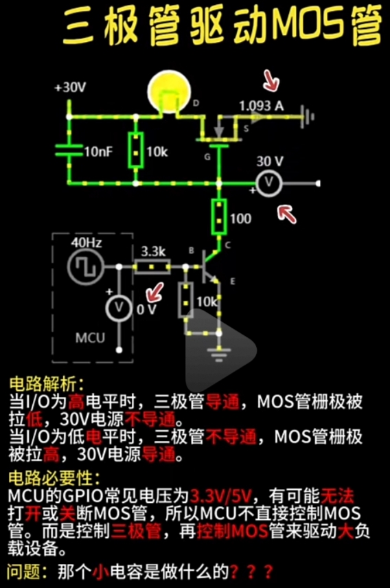
TL431应用实例: 充电器(TL431+MOS管充满自停)

MCU 或 OpAmp 用 三极管适配 以驱动 高Vgs电压的MOS管
下图电路解析:
当I/O为电平时,三极管导通 ,拉低MOS管G极
, 30V电源不导通;
当I/O为低电平时, 三极管不导通, 拉高MOS管栅极, 30V电源导通.
电路必要性:
MCU的GPIO( 或OpAmp输出) 电压(3.3V,5V) 无法直接控制(无法打开或关断)MOS管, 通过三极管适配能驱动M0S管带 大负载。
问题:那个小电容是做什么的?
大体原理:
-
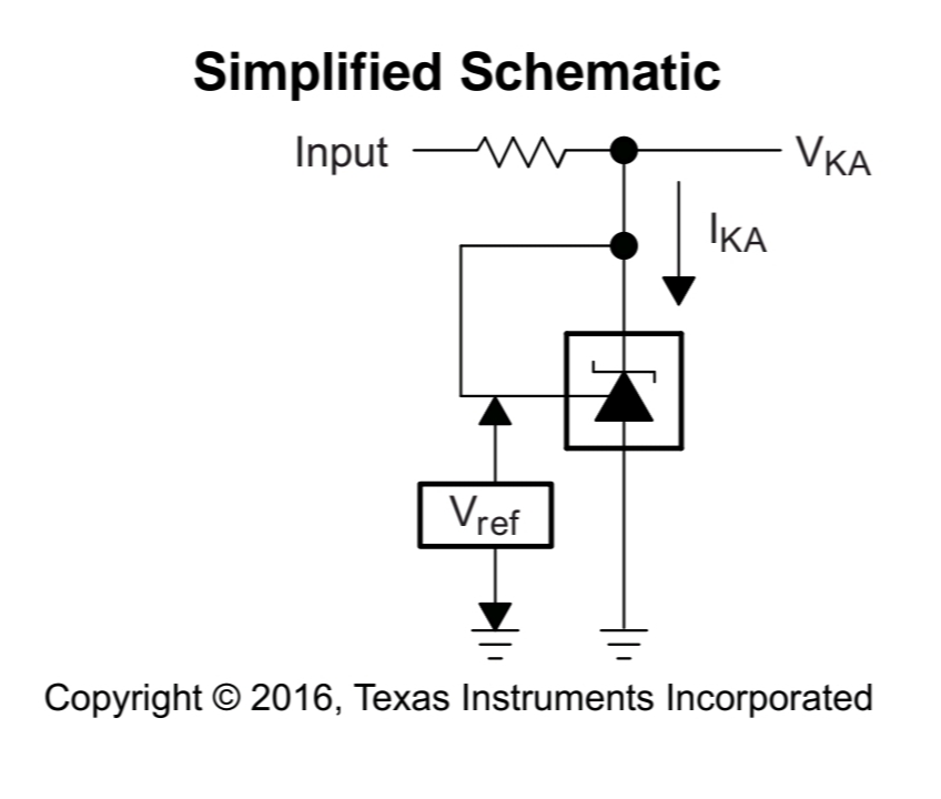
TL1431内部有“精准参考电压”、“放大器”与“消流器(由运放驱动的达林顿管消流1-100mA)”;
稳压原理:将pin REF输入的采样电压(多用串联的两个高精度电阻作为电压比例采样送入此REF引脚) 与 内部的Virtual Internal Pin精准稳定电压源进行比较,内部的OP AMP.放大此差值后,驱动连接在pin Cathode的内部达林顿管导通程度以对Vka(加在pin CATHODE与pin ANODE之间的电压)进行精准的负反馈式“旁路分流补偿”,最终实现稳压(Vka, Cathode与Anode两脚之间的电压,可通过经pin REF输入的信号电压的采样比例去调整)的目的. -
TL1431会将pin REF引脚的Vref电压钳位在2.5V的前提是运行时2.5V≤Vka≤36V 并且 1mA≤Ika≤100mA), Vka是Cathode与Anode的电位差,Ika是通过pin Cathode流过pin Andoe的电流; 因此通过采样比例用公式可以计算的到Vka值。
-
注意 pin CATHODE串接有 R 限流分压电阻,以使2.5V≤Vka≤36V 并且 1mA≤Ika≤100mA).
-
TL1431之所以能实现参考电压可调节, 是内外部元器件协同的作用;
外部的采样比例(两串联的精密电阻,调整 总阻值大小 与 两电阻的比例 就可以调整采样电压相对于Vka的比例); -
最终效果如同“简化电原理图”可将TL1431看做可调的动态稳压IC(仅当运行时2.5V≤Vka≤36V 并且 1mA≤Ika≤100mA)**;作为分流补偿式调压稳压器、误差放大器。
-
计算“动态稳压值”示例,
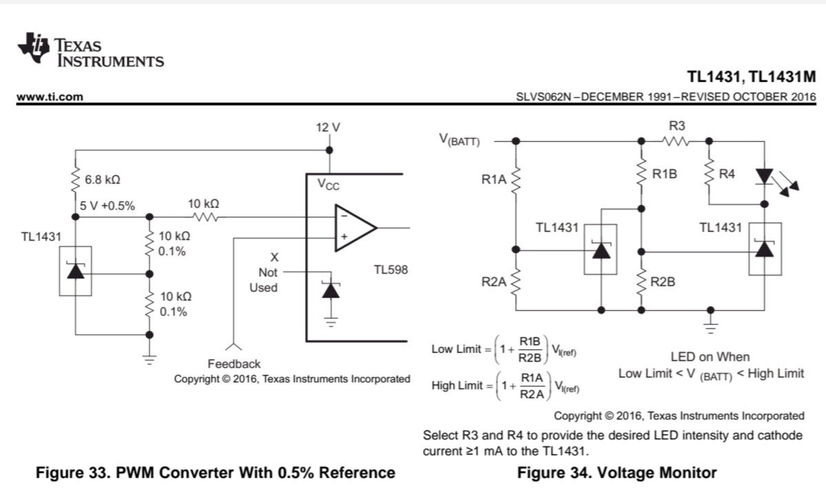
- 如下图上左侧的Fig.33 PWM Converter, TL1431之所Vka为5V,是因为:
- 采样比例为0.5(两个采样电阻都是10KΩ, 输入pin REF的电压是pin CATHODE电压Vka的一半);
- 内部精密基准电压是2.5V, 即通过TL431精准调整, 会将pin REF钳位在2.5V, 因此 2.5 / 0.5 得到Vka动态稳定在5V:
![]()
- 串接 一个电阻(限流分压)与 光电耦合器(隔离反馈) 在TL1431的pin CATHODE,并且将输出电压经过电阻比例采样与RC滤波输入pin REF,就是常用的开关电源反馈电路。
- 如下图上左侧的Fig.33 PWM Converter, TL1431之所Vka为5V,是因为:

-
请参考TI的Datasheet, 有非常完备的文档。
此处仅摘要。
The TL1431 device has proven ubiquity and versatility across a wide range of applications, ranging from powerto signal path.
This is due to its key components containing an accurate voltage reference and op amp, whichare very fundamental analog building blocks.
TL1431 is used in conjunction with its key components to behaveas a single voltage reference, error amplifier, voltage clamp, or comparator with integrated reference.
TL1431 can be operated and adjusted to cathode voltages from 2.5 V to 36 V, making this part optimum for a wide range of end equipments in industrial, auto, telecom, and computing.
In order for this device to behave as a shunt regulator or error amplifier, >1 mA (Imin(max)) must be supplied in to the cathode pin. Under this condition,feedback can be applied from the Cathode and Ref pins to create a replica of the internal reference voltage.
Various reference voltage options can be purchased with initial tolerances (at 25°C) of 0.4% and 1%. The TL1431C devices are characterized for operation from 0°C to 70°C, the TL1431Q devices are characterized foroperation from –40°C to 125°C, and the TL1431M devices are characterized for operation from –55°C to 125°C.- 概论:
![]()
- 详细描述:
![]()
- 概论:
-
TL431的大体原理+三个重要等效图:
大体原理:- TL1431 consists of an internal reference and amplifier that outputs a sink current base on the difference between the reference pin and the virtual internal pin.
- The sink current is produced by the internal Darlington pair, shown in Figure 22(F. B. Diagram, 功能模块电路图). A Darlington pair is used in order for this device to be able to sink a maximum current of 100 mA.
- TL1431 forces the reference pin to 2.5 V, when operated with enough voltage headroom (≥ 2.5 V) and cathode current (IKA). However, the reference pin can not be left floating, as it needs IREF ≥ 5 µA (see Electrical Characteristics – TL1431M). This is because the reference pin is driven into an npn, which needs base current to operate properly.
- When feedback is applied from the cathode and reference pins, TL1431 behaves as a Zenerdiode, regulating to a constant voltage dependent on current being supplied into the cathode. This is due to the internal amplifier and reference entering the proper operating regions. The same amount of current needed in the above feedback situation must be applied to this device in open loop, servo, or error amplifying implementationsin order for it to be in the proper linear region giving TL1431 enough gain.
- Unlike many linear regulators, TL1431 is internally compensated to be stable without an output capacitor between the cathode and anode. However, if desired an output capacitor can be used as a guide to assist in choosing the correct capacitor to maintain stability.


| 等效电路图 | 简化原理图 | 功能模块电路图 |
|---|---|---|
 |
 |
 |
2.常用封装:(注意都是“Top View顶视图”,包括 3pin TO92的):

-
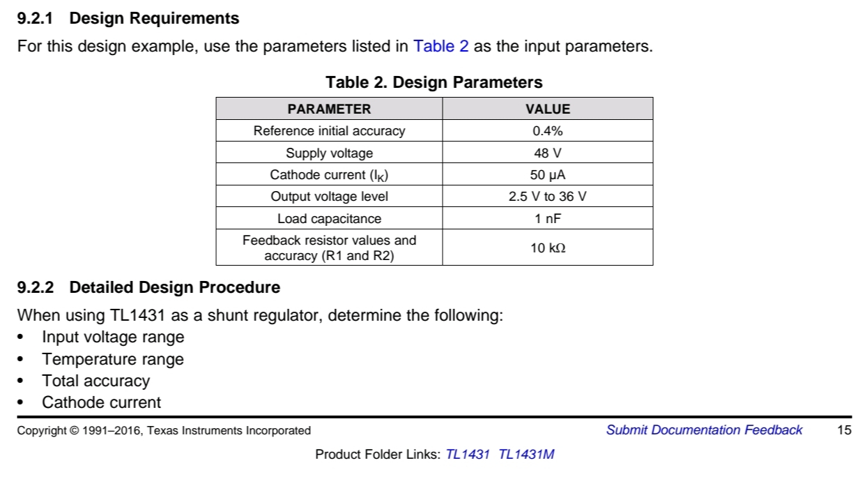
应用设计需求:
![]()
![]()
-
重要参数与电特性:
![]()
![]()
![]()
-
常用示例:
![]()
![]()
![]()
![]()


 浙公网安备 33010602011771号