SciTech-EECS-Circuits-JTAG协议背景知识简介与FTDI的FT4232H配成USB to JTAG TAP(MPSSE)使用实例
MPSSE Application Example:
http://ftdichip.cn/Support/SoftwareExamples/MPSSE.htm
MPSSE: AN_129 FTDI USB To JTAG TAP Example
MPSS: AN_114 FTDI USB to SPI Example
MPSSE: AN_113 FTDI USB to I2C Example
Application Notes/AN_129_FTDI_Hi_Speed_USB_To_JTAG_Example.pdf
FTDI MPSSE(Multi-Protocol Synchronous Serial Engine)
Using the MPSSE can simplify the synchronous serial protocol (USB to SPI, I2C, JTAG, etc.) design. This application note focuses on the hardware and software required to emulate a connection to a JTAG TAP test chain using the FT2232H. The FT232H and FT4232H can also be used with the example in this document, though pin-out and port selection will need to match the respective part.
Users can use the example schematic and functional software code to begin their design. The application example also duplicates the JTAG timing expected to be seen by the SN74BCT8244A to prove the function.
Note that software code listing is provided as an illustration only and not supported by FTDI.
1 Introduction
The FT2232H and FT4232H are the FTDI's first USB 2.0 Hi-Speed (480Mbits/s) USB to UART/FIFO ICs. They also have the capability of being configured in a variety of serial interfaces using the internal MPSSE. The FT2232H device has two independent ports, both of which can be configured to use the MPSSE while only Channel A and B of FT4232H can be configured to use the MPSSE. The FT232H, introduced in 2011, builds on the FTDI Hi-Speed USB family. The FT232H is a single-port UART/FIFO IC that has one MPSSE interface as well as several new modes.
1.1 FTDI MPSSE Introduction
The MPSSE is a feature of certain FTDI client ICs that allow emulation of several synchronous serial protocols including SPI, I2C and JTAG.
A single MPSSE is available in the FT2232D, a Full-Speed USB 2.0 client device. The FT2232D is capable of synchronous serial communication up to 6Mbps. As noted above, two MPSSEs are available in the FT2232H and the FT4232H, both Hi-Speed USB 2.0 client devices. Each of the engines is capable of synchronous serial communications up to 30Mbps. The MPSSE in the FT2232H and FT4232H provide new commands for additional clock modes and is used in CPU interface and synchronous FIFO (parallel) modes. The FT232H contains a single MPSSE, the CPU Synchronous FIFO and the new FT1248 modes. Application note AN_135, MPSSE Basics and AN_167, FT1248 Dynamic Parallel/Serial Interface Basics provide more information on these other modes.
This application note describes the use of the MPSSE to emulate a JTAG interface. There are multiple references to AN_108 - Command Processor for MPSSE and MCU Host Bus Emulation Modes, also available from the FTDI Web Site.
1.2 JTAG background
Today's electronic circuits consist of numerous complex integrated circuits. A typical embedded system can contain multiple CPUs, programmable devices, memory, etc. With such complexity, it is often impossible to directly probe and test the entire functionality of a given design.
In 1990, the IEEE(Institute of Electrical and Electronics Engineers) ratified the standard 1149.1, which was the work of the Joint Test Action Group (JTAG). This standard defines a common means of implementing boundary-scan test functionality in an integrated circuit. It allows devices from different vendors to be present in a common chain to provide access to all of the Input and Output (I/O) pins. Commonly used with additional facilities, such as a bed-of-nails device, it is possible to perform functional and manufacturing tests on an entire circuit. It is common to refer to the IEEE 1149.1 standard as the "JTAG standard". Many published documents and articles use these terms interchangeably.
The IEEE 1149.1 was most recently updated in 2001. Additional IEEE standards reference 1149.1 while providing expanded features such as analog circuit tests in addition to digital circuit tests. These additional standards are 1149.4 - Analog Boundary Scan, 1149.6 - Advanced I/O and 1532 - In System Configuration. The latter is commonly used for programming memory devices and configuring programmable digital logic such as FPGAs and CPLDs.
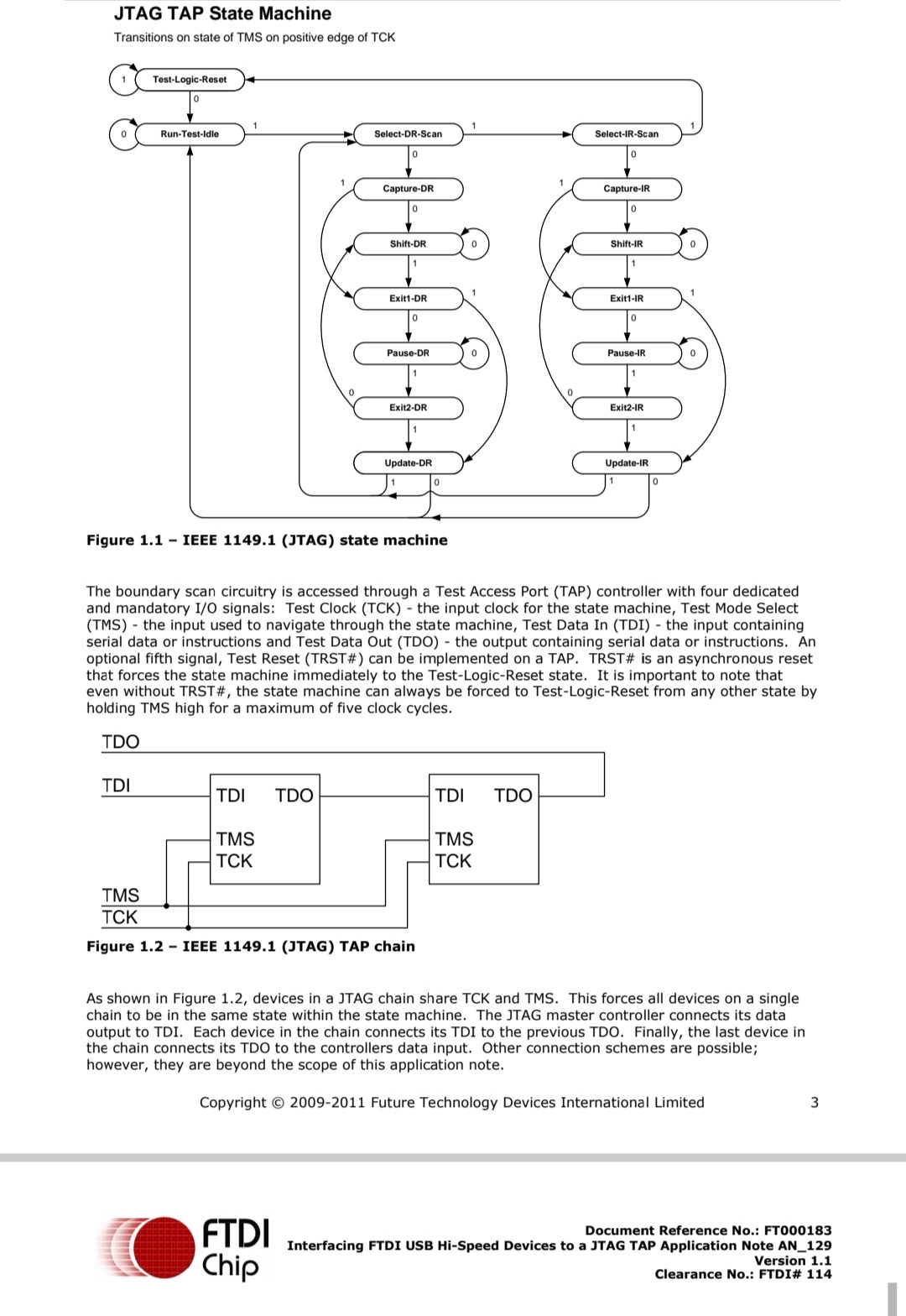
JTAG (IEEE 1149.1) defines a synchronous state machine consisting of 16 states as noted in Figure 1.1.
The boundary scan circuitry is accessed through a TAP(Test Access Port) controller with four dedicated and mandatory I/O signals:
TCK(Test Clock) - the input clock for the state machine,
TMS(Test Mode Select) - the input used to navigate through the state machine,
TDI(Test Data In) - the input containing serial data or instructions,
TDO(Test Data Out) - the output containing serial data or instructions.
TRST#(Test Reset) - An OPTIONAL fifth signal can be implemented on a TAP. TRST# is an asynchronous reset that forces the state machine immediately to the Test-Logic-Reset state. It is important to note that even without TRST#, the state machine can always be forced to Test-Logic-Reset from any other state by holding TMS high for a maximum of five clock cycles.
As shown in Figure 1.2, devices in a JTAG chain share TCK and TMS. This forces all devices on a single chain to be in the same state within the state machine:
- The JTAG master controller connects its data output to TDI.
- Each device in the chain connects its TDI to the previous TDO.
- Finally, the last device in the chain connects its TDO to the controllers data input.
- Other connection schemes are possible; however, they are beyond the scope of this application note.

 浙公网安备 33010602011771号