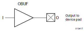
原语笔记:BuF系列
参考:
UG472
UG953
UG768
关于赛灵思FPGA中MMCME2_ADV与PLLE2_ADV的时钟原语学习与整理 - 知乎 (zhihu.com)
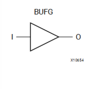
BUFG
Primitive: Global Clock Simple Buffer
介绍:
该设计元素是一个高扇出缓冲器,它将信号连接到全局布线资源,以实现信号的低偏斜分布。 BUFG 通常用在时钟网络以及其他高扇出网络(例如设置/重置和时钟使能)上。
简介:
全局缓冲,BUFG 的输出到达 FPGA 内部的 IOB、CLB、块 RAM 的时钟延迟和抖动最小。
模板
// BUFG: Global Clock Simple Buffer
//       7 Series
// Xilinx HDL Language Template, version 2023.2

BUFG_inst (
   .O(O), // 1-bit output: Clock output
   .I(I)  // 1-bit input: Clock input
);

// End of BUFG_inst instantiation
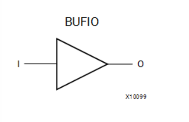
BUFIO
Primitive: Local Clock Buffer for I/O
介绍
该设计元素是本地时钟输入、时钟输出缓冲器。
它驱动 I/O 列内的专用时钟网络,独立于全局时钟资源,非常适合源同步数据捕获(转发/接收器时钟分配)。
BUFIO 元件可由位于同一时钟区域的专用 MRCC I/O 或能够为多个时钟区域提供时钟的 BUFMRCE/BUFMR 组件驱动。
BUFIO 只能驱动 I/O 组件所在的 Bank 内的组件。它们无法直接驱动逻辑资源(CLB、Block RAM 等),因为 I/O 时钟网络仅到达 I/O 列。
简介
BUFIO 是 IO 时钟网络,其独立于全局时钟资源,适合采集源同步数据。它只能驱动 IO Block 里面的逻辑,不能驱动 CLB 里面的 LUT,REG 等逻辑。
BUFIO 在采集源同步 IO 数据时,提供非常小的延时,因此非常适合采集比如 RGMII 接收侧的数据, 但是由于其不能驱动 FPGA 的内部逻辑,因此需要 BUFIO 和 BUFG 配合使用,以达到最佳性能。
模板
// BUFIO: Local Clock Buffer for I/O
//        7 Series
// Xilinx HDL Language Template, version 2023.2

BUFIO BUFIO_inst (
   .O(O), // 1-bit output: Clock output (connect to I/O clock loads).
   .I(I)  // 1-bit input: Clock input (connect to an IBUF or BUFMR).
);

// End of BUFIO_inst instantiation
BUFR
介绍
BUFR 是 7 系列器件中的区域时钟缓冲器,可将时钟信号驱动到时钟区域内的专用时钟网络,独立于全局时钟树。
每个BUFR可以驱动其所在区域的区域时钟网络。与 BUFIO 组件不同,BUFR 组件可以驱动现有时钟区域中的 I/O 逻辑和逻辑资源(CLB、块 RAM 等)。
它们可由 IBUF、BUFMRCE、MMCM 或本地互连的输出驱动,并且能够生成相对于时钟输入的分频时钟输出。
除法值是 1 到 8 之间的整数。 BUFR 组件非常适合需要时钟域交叉或串并转换的源同步应用。
典型时钟区域(两个区域时钟网络)中有两个 BUFR 组件。
如果多个时钟区域需要本地时钟,则 BUFMRCE 可以驱动相邻时钟区域中的多个 BUFR 组件,以进一步扩展此时钟功能。有关更多详细信息,请参阅 BUFMRCE。
简介
BUFR 是 regional 时钟网络,它的驱动范围只能局限在一个 clock region 的逻辑。BUFR 相比 BUFG 的最大优势是偏斜和功耗都比较小。
模板:
// BUFR: Regional Clock Buffer for I/O and Logic Resources within a Clock Region
//       7 Series
// Xilinx HDL Language Template, version 2023.2

BUFR #(
   .BUFR_DIVIDE("BYPASS"),   // Values: "BYPASS, 1, 2, 3, 4, 5, 6, 7, 8"
   .SIM_DEVICE("7SERIES")  // Must be set to "7SERIES"
)
BUFR_inst (
   .O(O),     // 1-bit output: Clock output port
   .CE(CE),   // 1-bit input: Active high, clock enable (Divided modes only)
   .CLR(CLR), // 1-bit input: Active high, asynchronous clear (Divided modes only)
   .I(I)      // 1-bit input: Clock buffer input driven by an IBUF, MMCM or local interconnect
);

// End of BUFR_inst instantiation
IBUF
Primitive: Input Buffer
Introduction
This design element is automatically inserted (inferred) by the synthesis tool to any signal directly connected to a top-level input or in-out port of the design. You should generally let the synthesis tool infer this buffer. However, it can be instantiated into the design if required. In order to do so, connect the input port (I) directly to the associated top-level input or in-out port, and connect the output port (O) to the logic sourced by that port. Modify any necessary generic maps (VHDL) or named parameter value assignment (Verilog) to change the default behavior of the component.
该设计元素由综合工具自动插入(推断)到直接连接到设计的顶级输入或输入输出端口的任何信号。
通常您应该让综合工具推断此缓冲区。
但是,如果需要,可以将其实例化到设计中。
为此,请将输入端口 (I) 直接连接到关联的顶级输入或输入输出端口,并将输出端口 (O) 连接到由该端口提供的逻辑。修改任何必要的通用映射 (VHDL) 或命名参数值分配 (Verilog) 以更改组件的默认行为。
OBUF
Primitive: Output Buffer
Introduction
This design element is a simple output buffer used to drive output signals to the FPGA device pins that do not need to be 3-stated (constantly driven). Either an OBUF, OBUFT, OBUFDS, or OBUFTDS must be connected to every output port in the design.
This element isolates the internal circuit and provides drive current for signals leaving a chip. It exists in input/output blocks (IOB). Its output (O) is connected to an OPAD or an IOPAD. The interface standard used by this element is LVCMOS18. Also, this element has selectable drive and slew rates using the DRIVE and SLOW or FAST constraints.
该设计元素是一个简单的输出缓冲器,用于将输出信号驱动到不需要三态(持续驱动)的 FPGA 器件引脚。
OBUF、OBUFT、OBUFDS 或 OBUFTDS 必须连接到设计中的每个输出端口。
该元件隔离内部电路并为离开芯片的信号提供驱动电流。它存在于输入/输出块(IOB)中。
其输出 (O) 连接到 OPAD 或 IOPAD。该元件使用的接口标准是LVCMOS18。此外,该元件还具有使用 DRIVE 和 SLOW 或 FAST 约束条件可选择的驱动和转换速率。

 浙公网安备 33010602011771号