Xilinx实现以太网MAC RGMII相关原语
1、RX方向:IDDR
IDDR
IDDR原语
IDDR #(
    .DDR_CLK_EDGE("OPPOSITE_EDGE"), // "OPPOSITE_EDGE", "SAME_EDGE" or "SAME_EDGE_PIPELINED"
    .INIT_Q1(1'b0), // Initial value of Q1: 1'b0 or 1'b1
    .INIT_Q2(1'b0), // Initial value of Q2: 1'b0 or 1'b1
    .SRTYPE("SYNC") // Set/Reset type: "SYNC" or "ASYNC"
) IDDR_inst (
    .Q1(Q1), // 1-bit output for positive edge of clock
    .Q2(Q2), // 1-bit output for negative edge of clock
    .C(C), // 1-bit clock input
    .CE(CE), // 1-bit clock enable input
    .D(D), // 1-bit DDR data input
    .R(R), // 1-bit reset
    .S(S) // 1-bit set
);
参数DDR_CLK_EDGE 为 IDDR 的三种采集模式:
- “OPPOSITE_EDGE”:RGMII采用
- “SAME_EDGE”
- “SAME_EDGE_PIPELINED”
OPPOSITE_EDGE 模式的时序图如下图所示: OPPOSITE_EDGE 模式下, 在时钟的上升沿输出的 Q1, 时钟的下降沿输出 Q2。
SAME_EDGE 模式的时序图如下图所示:
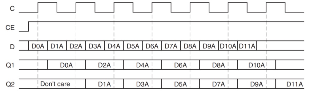
图 27.1.17 IDDR“SAME_EDGE”模式时序图
SAME_EDGE 模式下,在时钟的上升沿输出 Q1 和 Q2,但 Q1 和 Q2 不在同一个 cycle 输出。
SAME_EDGE_PIPELINED 模式的时序图如下图所示: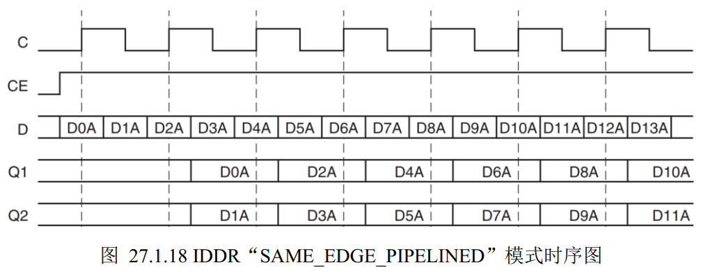
SAME_EDGE_PIPELINED 模式下,在时钟的上升沿输出 Q1 和 Q2, Q1 和 Q2 虽然在同一个 cycle 输出,但整体延时了一个时钟周期。在使用 IDDR 时,一般采用此种模式。
2、IDELAY

IDELAYE2端口
| Port Name | Direction | Width | Function |
| C | Input | 1 |
Clock input used in VARIABLE, VAR_LOAD, or VAR_LOAD_PIPE mode. C can be locally inverted, and must be supplied by a global or regional clock buffer. 备注:FIXED mode则不需要这个Clock,RGMII一般采用FIXED mode,所以不需要这个Clock。 |
| REGRST | Input | 1 | Reset for the pipeline register. Only used in VAR_LOAD_PIPE mode. |
| LD | Input | 1 |
Loads the IDELAYE2 primitive to the pre-programmed value in VARIABLE mode. In VAR_LOAD mode, it loads the value of CNTVALUEIN. In VAR_LOAD_PIPE mode it loads the value currently in the pipeline register. |
| CE | Input | 1 | Enable increment/decrement function. |
| INC | Input | 1 | Increment/decrement number of tap delays. |
| CINVCTRL | Input | 1 | Dynamically inverts the clock (C) polarity. |
| CNTVALUEIN | Input | 5 | Counter value from FPGA logic for dynamically loadable tap value. |
| IDATAIN | Input | 1 |
Data input for IDELAY from the IBUF. 备注:IBUF:将IOB输入管脚送入FPGA内部,OBUF:将输出信号送出FPGA输出管脚。 |
| DATAIN | Input | 1 | Data input for IDELAY from the FPGA logic. |
| LDPIPEEN | Input | 1 | Enables the pipeline register to load data. |
| DATAOUT | Output | 1 | Delayed data from one of two data input ports (IDATAIN or DATAIN). |
| CNTVALUEOUT | Output | 5 |
Counter value going to FPGA logic for monitoring tap value. 备注:该输出可以实时监测delay tap。 |
参考资料:
3、http://www.360doc.com/content/21/0421/20/9204498_973469071.shtml
4、https://blog.csdn.net/qq_40268672/article/details/122159654

 浙公网安备 33010602011771号