spill register/pipeline skid buffer学习
spill register/pipeline skid buffer学习
概述
skid buffer(滑动缓冲区)是一种用于实现背靠背传输的技术之一。通过使用滑动缓冲区,可以在发送方和接收方之间实现流水线传输,并在数据到达接收方之前将其暂时存储在缓冲区中。这样,即使发送方和接收方之间没有组合逻辑路径,也能够实现背靠背传输。在使用AXI总线时经常应用。

Decouples two sides of a ready/valid handshake to allow back-to-back transfers without a combinational path between input and output, thus pipelining the path. Can function as a two-entry Circular Buffer.
A skid buffer is the smallest Pipeline FIFO Buffer, with only two entries. It is useful when you need to pipeline the path between a sender and a receiver for concurrency and/or timing, but not to smooth-out data rate mismatches. It also only requires two data registers, which at this scale is smaller than LUTRAMs or Block RAMs (depending on implementation), and has more freedom of placement and routing.
Alternately, a Skid Buffer is also known as a Carloni Buffer. For reference, see Abbas and Betz "Latency Insensitive Design Styles for FPGAs" (FPL, 2018).


跟ping-pong缓冲还是有一点点像。2级寄存器,平时当下游ready,第一个寄存器输出给下游;而当下游ready拉低时,第一个寄存器的值放到第二个,而上游还valid的数据放到第一个,这样就实现了在ready打拍的基础上而吞吐率没有损失(不过还是有延迟就是了)。
使用skid buffer避免了ready信号以组合逻辑一直向上传递的问题。
如下图是一个直接握手反压的过程,其中ready信号以组合逻辑一直向上游传递。

尝试解释
首先要提高频率,流水线中ready路径不能是纯组合路径,需要插入寄存器来改善时钟和扇出。但如果只有一级寄存器,会造成流水线吞吐率降低的问题。当平时下游ready为高时流水线正常流动,当不能接收数据了,ready拉低,此时对于缓冲区其中有数据,但不能发送给下游。上游还没接收到ready拉低的信号,如果写入缓冲区则会造成数据丢失;如果不写入,也阻塞的话,又会浪费一个时钟。
而这时2个寄存器就可以解决这个问题,当下游ready突然拉低,第一个寄存器的值可以放到第二个,而上游的值可以放到第一个,这样就保证了ready打拍的基础上,又没有损失吞吐率。
代码
这里我学习spill_register
module spill_register_flushable #(
  parameter type T           = logic,
  parameter bit  Bypass      = 1'b0   // make this spill register transparent
) (
  input  logic clk_i   ,
  input  logic rst_ni  ,
  input  logic valid_i ,
  input  logic flush_i ,
  output logic ready_o ,
  input  T     data_i  ,
  output logic valid_o ,
  input  logic ready_i ,
  output T     data_o
);

  if (Bypass) begin : gen_bypass
    assign valid_o = valid_i;
    assign ready_o = ready_i;
    assign data_o  = data_i;
  end else begin : gen_spill_reg
    // The A register.
    T a_data_q;
    logic a_full_q;
    logic a_fill, a_drain;

    always_ff @(posedge clk_i or negedge rst_ni) begin : ps_a_data
      if (!rst_ni)
        a_data_q <= '0;
      else if (a_fill)
        a_data_q <= data_i;
    end

    always_ff @(posedge clk_i or negedge rst_ni) begin : ps_a_full
      if (!rst_ni)
        a_full_q <= 0;
      else if (a_fill || a_drain)
        a_full_q <= a_fill;
    end

    // The B register.
    T b_data_q;
    logic b_full_q;
    logic b_fill, b_drain;

    always_ff @(posedge clk_i or negedge rst_ni) begin : ps_b_data
      if (!rst_ni)
        b_data_q <= '0;
      else if (b_fill)
        b_data_q <= a_data_q;
    end

    always_ff @(posedge clk_i or negedge rst_ni) begin : ps_b_full
      if (!rst_ni)
        b_full_q <= 0;
      else if (b_fill || b_drain)
        b_full_q <= b_fill;
    end

    // Fill the A register when the A or B register is empty. Drain the A register
    // whenever it is full and being filled, or if a flush is requested.
    assign a_fill = valid_i && ready_o && (!flush_i);
    assign a_drain = (a_full_q && !b_full_q) || flush_i;

    // Fill the B register whenever the A register is drained, but the downstream
    // circuit is not ready. Drain the B register whenever it is full and the
    // downstream circuit is ready, or if a flush is requested.
    assign b_fill = a_drain && (!ready_i) && (!flush_i);
    assign b_drain = (b_full_q && ready_i) || flush_i;

    // We can accept input as long as register B is not full.
    // Note: flush_i and valid_i must not be high at the same time,
    // otherwise an invalid handshake may occur
    assign ready_o = !a_full_q || !b_full_q;

    // The unit provides output as long as one of the registers is filled.
    assign valid_o = a_full_q | b_full_q;

    // We empty the spill register before the slice register.
    assign data_o = b_full_q ? b_data_q : a_data_q;

    `ifndef SYNTHESIS
    `ifndef COMMON_CELLS_ASSERTS_OFF
    flush_valid : assert property (
      @(posedge clk_i) disable iff (~rst_ni) (flush_i |-> ~valid_i)) else
      $warning("Trying to flush and feed the spill register simultaneously. You will lose data!");
   `endif
     `endif
  end
endmodule
框图就如上图所示。其中有2级寄存器a和b,然后将上游的valid和下游的ready作为输入产生控制信号。
其中控制信号如下:

其中ready_o是当2级寄存器都不满时置起来,这样就对ready_i打了一拍。当ready_i由1变0,还有一个寄存器可以放,要等到时钟沿ready_o才会变;当ready_i由0变1,可以输出给下游,full信号会在时钟沿变,ready_o也就在时钟沿才会变。
同样,valid_o是a和b寄存器有一个为满就置起来,这样当valid_i变化,full信号需要在时钟沿变化,valid_o就打了一拍。
当a有数据 并且 b空 并且下游不ready时 将a的数据放入b中,这样就能将上游的数据放入a中,而当下游ready后优先将b的数据输出。
仿真
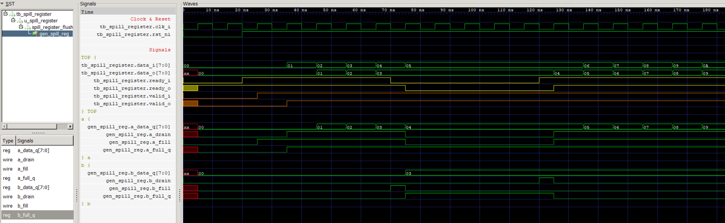
这里我模拟了下游开始一直ready,而过了一段时间不能再接收了,ready拉低,而上游还是valid的情况。
可以看到valid、ready信号被打拍了
并且没有数据丢失,并且吞吐率没有降低。
并且我们可以观察到ready_o和ready_i之间有一拍,这样避免了ready信号以组合逻辑一直向上传递的问题。

 浙公网安备 33010602011771号