clocking block
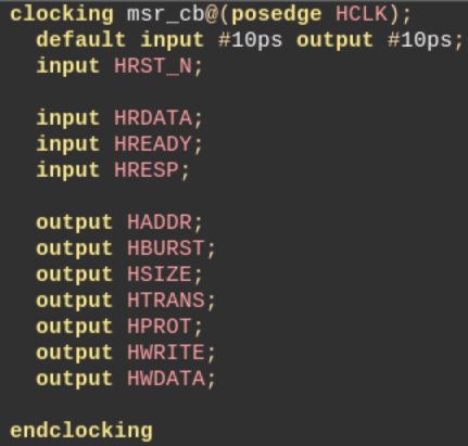
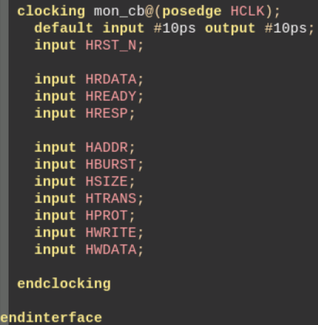
default input #10ps output #10ps
input 延迟10ps驱动,相当于input的signal波形往后推迟10ps,而clk不变,则等价于clk提前10ps采样signal;
output延迟10ps驱动,即驱动落后。
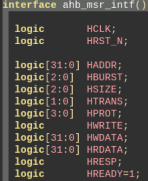
下图为interface,msr_cb,mon_cb上的HTRANS波形图。可以看到driver_cb和mon_cb的信号与clk对齐。
cursor time时刻(黄线):interface上的HTRANS=2 ,msr_cb上的HTRANS=2, mon_cb上的HTRANS=2 为什么呢?
为什么没有延迟10ps?因为interface上的信号是由msr_cb里的信号进行驱动的,msr_cb里的信号在clk上升沿驱动后,信号到了interface上,10ps最终反映在interface上,不在msr_cb块里。
那为什么mon_cb里的信号比driver的信号晚一拍呢?因为msr_cb里的信号驱动到interface上后,monitor进行采样,在cursor time时刻的前10ps,mon_cb块进行采样,故在cursor time时刻的前10ps,mon_cb上的HTRANS=2,在cursor time时刻将采样的信号反应在波形上。
There is nothing wrong; the simulation behaves as expected. The clocking block applies the 4ns delay to the output as expected and as seen in your waves.
However, the clocking block does not apply any delay to the input. The clocking block samples the input before the rising clock edge. Refer to IEEE Std 1800-2017, section 14.4 Input and output skews:
Input (or inout) signals are sampled at the designated clock event. If an input skew is specified, then the signal is sampled at skew time units before the clock event. Similarly, output (or inout) signals are driven skew simulation time units after the corresponding clock event.
Since you specified 1step, the input is sampled 100ps before the rising edge of the clock. One step is equal to the timeprecision. The sampling point will not be visible in the waveforms since it is not a separate signal.

interface clocking block使用 及 verdi capture delta cycle_verdi delta cycle_劲仔小鱼的博客-CSDN博客
Systemverilog Academy https://www.youtube.com/watch?v=SezmL9cs
https://electronics.stackexchange.com/questions/586642/why-dont-i-see-the-clocking-block-input-skew-in-waveforms

 浙公网安备 33010602011771号