
Intel GEN9 GPU
SGEMM for Intel® Processor Graphics
The size of subgroup is equal to SIMD width (note that code targeting Intel® Processor Graphics can be compiled SIMD-8, SIMD-16, or SIMD-32 depending on the size of the kernel, which means that 8, 16 or 32 work items respectively can fit on a hardware thread of the Execution Unit (EU). For a deeper introduction please see section 5.3.5 SIMD Code Generation for SPMD Programming Models of Stephen Junkins’ excellent paper “The Compute Architecture of Intel® Processor Graphics Gen8” ). For example if the kernel is compiled SIMD-8, then a subgroup is made up of 8 work items that share 4 KB of register space of a hardware thread and execute together. The programmers could use a kernel function get_sub_group_size to figure out the size of the subgroup.
4 SOC ARCHITECTURE
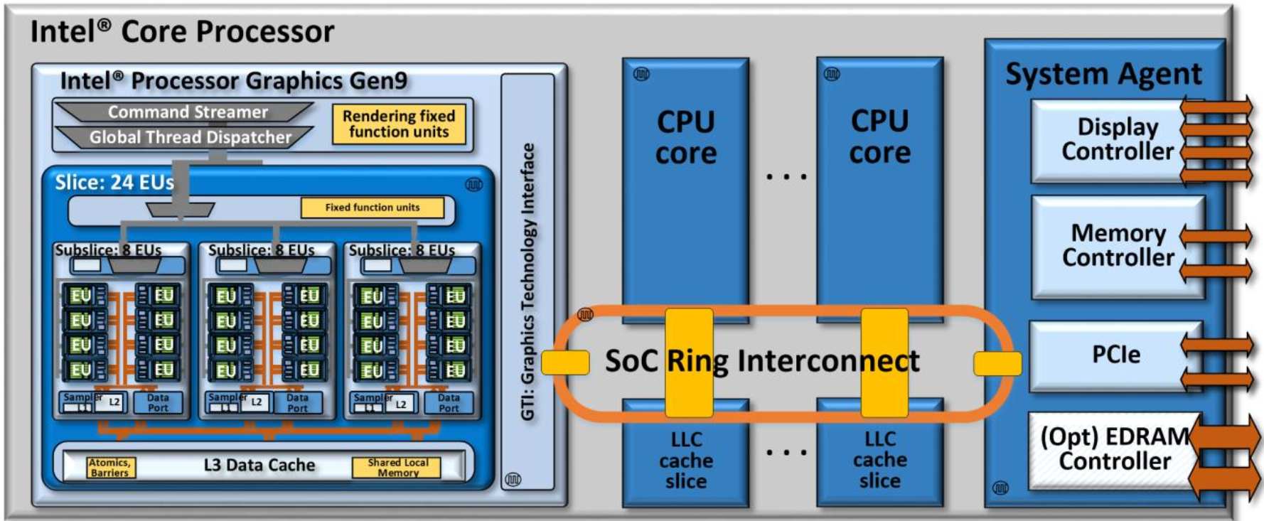
An Intel® Core™ i7 processor 6700K SoC and its ring interconnect architecture.
4.1 SOC ARCHITECTURE
Intel 6th generation Core processors are complex SoCs integrating multiple CPU cores, Intel processor graphics, and potentially other fixed functions all on a single shared silicon die. The architecture implements multiple unique clock domains, which have been partitioned as a perCPU core clock domain, a processor graphics clock domain, and a ring interconnect clock domain. The SoC architecture is designed to be extensible for a range of products, and yet still enable efficient wire routing between components within the SoC.
Intel第六代Core处理器是复杂的SoC,在单个共享的硅芯片上集成了多个CPU内核,Intel处理器图形以及可能的其他固定功能。 该体系结构实现了多个唯一的时钟域,这些时钟域已被划分为perCPU核心时钟域,处理器图形时钟域和环形互连时钟域。 SoC体系结构被设计为可扩展为适用于多种产品,但仍可在SoC内部组件之间实现有效的布线。
4.2 RING INTERCONNECT
The on-die bus between CPU cores, caches, and Intel processor graphics is a ring based topology with dedicated local interfaces for each connected “agent”. This SoC ring interconnect is a bi-directional ring that has a 32-byte wide data bus, with separate lines for request, snoop, and acknowledge. Every on-die CPU core is regarded as a unique agent.
Similarly, Intel processor graphics is treated as a unique agent on the interconnect ring. A system agent is also connected to the ring, which bundles the DRAM memory management unit, display controller, and other off chip I/O controllers such as PCI Express*. Importantly, all off-chip system memory transactions to/from CPU cores and to/from Intel processor graphics are facilitated by this interconnect, through the system agent, and the unified DRAM memory controller
CPU内核,缓存和Intel处理器图形之间的片上总线是基于环的拓扑,具有用于每个连接的“代理”的专用本地接口。 SoC环互连是一个双向环,具有32字节宽的数据总线,并带有用于请求,侦听和确认的单独线路。 每个片上CPU内核都被视为唯一的代理。
同样,英特尔处理器图形被视为互连环上的唯一代理。 系统代理也连接到该环,该环捆绑了DRAM内存管理单元,显示控制器和其他片外I / O控制器,例如PCI Express *。 重要的是,这种互连,通过系统代理和统一的DRAM存储器控制器,可以方便地实现往返于CPU内核和往返于英特尔处理器图形的所有片外系统内存事务。
4.3 SHARED LLC
Some SoC products include a shared Last Level Cache (LLC) that is also connected to the ring. In such SoCs, each on-die core is allocated a slice of cache, and that cache slice is connected as a unique agent on the ring. However, all of the slices work together as a single cache, albeit a shared and distributed cache. An address hashing scheme routes data requests to the cache slice assigned to its address. This distributed LLC is also shared with Intel processor graphics. For both CPU cores and for Intel processor graphics, LLC seeks to reduce apparent latency to system DRAM and to provide higher effective bandwidth.
某些SoC产品包括一个共享的末级缓存(LLC),该缓存也已连接到环网。 在此类SoC中,每个管芯上的内核都分配了一个高速缓存片,并且该高速缓存片作为环上的唯一代理连接。 但是,所有切片都可以作为单个缓存一起工作,即使共享和分布式缓存也是如此。 地址哈希方案将数据请求路由到分配给其地址的缓存片。 此分布式LLC也与Intel处理器图形共享。 对于CPU内核和Intel处理器图形,LLC都希望减少系统DRAM的明显等待时间,并提供更高的有效带宽。
4.4 OPTIONAL EDRAM
Some SoC products may include 64-128 megabytes of embedded DRAM (EDRAM), bundled into the SoC’s chip packaging. For example, the Intel processor graphics gen8 based Intel Iris Pro 6200 products bundle a 128 megabyte EDRAM. The EDRAM operates in its own clock domain and can be clocked up to 1.6GHz. The EDRAM has separate buses for read and write, and each are capable of 32 byte/EDRAM-cycle. EDRAM supports many applications including low latency display surface refresh. For the compute architecture of Intel processor graphics gen9, EDRAM further supports the memory hierarchy by serving as a “memory-side” cache between LLC and DRAM. Like LLC, EDRAM caching is shared by both Intel processor graphics and by CPU cores. On an LLC or EDRAM cache miss, data from DRAM will be filled first into EDRAM. (An optional mode also allows bypass to LLC.) Conversely, as cachelines are evicted from LLC, they will be written back into EDRAM. If compute kernels wish to read or write cachelines currently stored in EDRAM, they are quickly re-loaded into LLC, and read/writing then proceeds as usual.
某些SoC产品可能包括捆绑在SoC芯片封装中的64-128 MB嵌入式DRAM(EDRAM)。例如,基于Intel gen8处理器图形的Intel Iris Pro 6200产品捆绑了128 MB EDRAM。 EDRAM在其自己的时钟域中运行,最高时钟频率为1.6GHz。 EDRAM具有用于读取和写入的单独总线,并且每个总线能够支持32字节/ EDRAM周期。 EDRAM支持许多应用程序,包括低延迟的显示表面刷新。对于第9代英特尔处理器图形的计算架构,EDRAM通过充当LLC和DRAM之间的“内存侧”缓存来进一步支持内存层次结构。与LLC一样,EDRAM缓存由Intel处理器图形和CPU内核共享。在LLC或EDRAM高速缓存未命中时,来自DRAM的数据将首先填充到EDRAM中。 (可选模式也允许绕过LLC。)相反,随着从LLC撤出高速缓存行,它们将被写回到EDRAM。如果计算内核希望读取或写入当前存储在EDRAM中的高速缓存行,则将它们迅速重新加载到LLC中,然后像往常一样进行读取/写入
Look for more details about Intel processor graphics gen9-based products with EDRAM in future product announcements.
在将来的产品公告中查找有关带有EDRAM的基于Intel gen9处理器的产品的更多详细信息。
5 THE COMPUTE ARCHITECTURE OF INTEL PROCESSOR GRAPHICS GEN9
5.1 NEW CHANGES FOR INTEL PROCESSOR GRAPHICS GEN9
Intel processor graphics gen9 includes many refinements throughout the micro architecture and supporting software, over Intel processor graphics gen8. Generally, these changes are across the domains of memory hierarchy, compute capability, and product configuration. They are briefly summarized here, with more detail integrated throughput the paper.
英特尔处理器图形gen9在微体系结构和支持软件方面进行了许多改进,比英特尔处理器图形gen8更好。 通常,这些更改涉及内存层次结构,计算能力和产品配置的各个领域。 它们在此处进行了简要总结,并在本文中更详细地介绍了集成吞吐量。
Gen9 Memory Hierarchy Refinements:
Coherent SVM write performance is significantly improved via new LLC cache management policies.
The available L3 cache capacity has been increased to 768 Kbytes per slice (512 Kbytes for application data).
The sizes of both L3 and LLC request queues have been increased. This improves latency hiding to achieve better effective bandwidth against the architecture peak theoretical.
In Gen9 EDRAM now acts as a memory-side cache between LLC and DRAM. Also, the EDRAM memory controller has moved into the system agent, adjacent to the display controller, to support power efficient and low latency display refresh.
Texture samplers now natively support an NV12 YUV format for improved surface sharing between compute APIs and media fixed function units
Gen9内存层次结构改进:
通过新的LLC缓存管理策略,相干SVM的写入性能得到了显着改善。
可用的L3缓存容量已增加到每片768 KB(应用程序数据为512 KB)。
L3和LLC请求队列的大小均已增加。 这样可以改善延迟隐藏,从而针对架构峰值理论值获得更好的有效带宽。
在Gen9中,EDRAM现在充当LLC和DRAM之间的内存侧缓存。 同样,EDRAM存储器控制器已移入系统代理,与显示控制器相邻,以支持省电且低延迟的显示刷新。
纹理采样器现在原生支持NV12 YUV格式,以改善计算API和媒体固定功能单元之间的表面共享。
Gen9 Compute Capability Refinements:
Preemption of compute applications is now supported at a thread level, meaning that compute threads can be preempted (and later resumed) midway through their execution.
Round robin scheduling of threads within an execution unit.
Gen9 adds new native support for the 32-bit float atomics operations of min, max, and compare/exchange. Also the performance of all 32-bit atomics is improved for kernel scenarios that issued multiple atomics back to back.
16-bit floating point capability is improved with native support for denormals and gradual underflow.
Gen9 Product Configuration Flexibility:
Gen9 has been designed to enable products with 1, 2 or 3 slices.
Gen9 adds new power gating and clock domains for more efficient dynamic power management. This can particularly improve low power media playback modes.
Gen9计算能力优化:
现在在线程级别支持抢占计算应用程序,这意味着可以在执行计算过程中抢占(然后恢复)计算线程。
执行单元内线程的循环调度。
Gen9为最小,最大和比较/交换的32位浮点原子操作添加了新的本机支持。 此外,对于内核场景(背对背发出多个原子),所有32位原子的性能也得到了改善。
通过对异常和渐进下溢的本机支持,改进了16位浮点功能。
Gen9产品配置灵活性:
Gen9旨在支持具有1、2或3片的产品。
Gen9添加了新的电源门控和时钟域,以实现更有效的动态电源管理。 这可以特别改善低功耗媒体播放模式。
5.2 MODULAR DESIGN FOR PRODUCT SCALABILITY
The gen9 compute architecture is designed for scalability across a wide range of target products. The architecture’s modularity enables exact product targeting to a particular market segment or product power envelope. The architecture begins with compute components called execution units. Execution units are clustered into groups called subslices. Subslices are further clustered into slices. Together, execution units, subslices, and slices are the modular building blocks that are composed to create many product variants based upon Intel processor graphics gen9 compute architecture. Some example variants are shown in Figure 6, Figure 7, and in Figure 8. The following sections describe the architecture components in detail, and show holistically how they may be composed into full products.
gen9计算体系结构旨在实现跨多种目标产品的可伸缩性。 该架构的模块化特性可将产品精确定位到特定细分市场或产品功率范围。 该架构始于称为执行单元的计算组件。 执行单元分为称为子切片的组。 子切片进一步聚集成切片。 执行单元,子切片和切片一起构成了模块化的构建基块,这些模块可根据英特尔处理器图形gen9计算架构创建许多产品变体。 图6,图7和图8中显示了一些示例变体。以下各节详细描述了体系结构组件,并全面显示了它们如何组成完整的产品。
5.3 EXECUTION UNIT (EUS) ARCHITECTURE
The foundational building block of gen9 compute architecture is the execution unit, commonly abbreviated as EU. The architecture of an EU is a combination of simultaneous multi-threading (SMT) and fine-grained interleaved multi-threading (IMT). These are compute processors that drive multiple issue, single instruction, multiple data arithmetic logic units (SIMD ALUs) pipelined across multiple threads, for high-throughput floating-point and integer compute. The fine-grain threaded nature of the EUs ensures continuous streams of ready to execute
instructions, while also enabling latency hiding of longer operations such as memory scatter/gather, sampler requests, or other system communication.
gen9计算体系结构的基本构建块是执行单元,通常缩写为EU。 EU的体系结构是同时多线程(SMT)和细粒度交错多线程(IMT)的组合。 这些是计算处理器,可驱动跨多个线程流水线化的多个问题,单指令,多个数据算术逻辑单元(SIMD ALU),以实现高吞吐量的浮点和整数计算。 EU的细粒度线程特性确保了准备执行指令的连续流,同时还可以隐藏较长的操作(例如内存分散/收集,采样器请求或其他系统通信)的延迟。
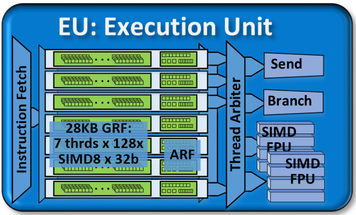
The Execution Unit (EU). Each gen9 EU has seven threads. Each thread has 128 SIMD-8 32-bit registers (GRF) and supporting architecture specific registers (ARF). The EU can co-issue to four instruction processing units including two FPUs, a branch unit, and a message send unit.
执行单位(EU)。 每个gen9 EU都有七个线程。 每个线程具有128个SIMD-8 32位寄存器(GRF)和支持特定于体系结构的寄存器(ARF)。 EU可以共同发布四个指令处理单元,包括两个FPU,一个分支单元和一个消息发送单元。
Product architects may fine-tune the number of threads and number of registers per EU to match scalability and specific product design requirements. For gen9-based products, each EU thread has 128 general purpose registers. Each register stores 32 bytes, accessible as a SIMD 8-element vector of 32-bit data elements. Thus each gen9 thread has 4 Kbytes of general purpose register file (GRF). In the gen9 architecture, each EU has seven threads for a total of 28 Kbytes of GRF per EU. Flexible addressing modes permit registers to be addressed together to build effectively wider registers, or even to represent strided rectangular block data structures. Per-thread architectural state is maintained in a separate dedicated architecture register file (ARF).
产品架构师可以微调每个EU的线程数和寄存器数,以匹配可伸缩性和特定的产品设计要求。 对于基于Gen9的产品,每个EU线程都有128个通用寄存器。 每个寄存器存储32个字节,可以将其作为32位数据元素的SIMD 8元素向量进行访问。 因此,每个gen9线程都有4 KB的通用寄存器文件(GRF)。 在gen9架构中,每个EU都有七个线程,每个EU总共有28 KB GRF。 灵活的寻址模式允许将寄存器一起寻址,以有效地构建更宽的寄存器,甚至代表跨步的矩形块数据结构。 每个线程的架构状态都在单独的专用架构寄存器文件(ARF)中维护。
5.3.1 Simultaneous Multi-Threading and Multiple Issue Execution
Depending on the software workload, the hardware threads within an EU may all be executing the same compute kernel code, or each EU thread could be executing code from a completely different compute kernel. The execution state of each thread, including its own instruction pointers, are held in thread-specific ARF registers.
On every cycle, an EU can co-issue up to four different instructions, which must be sourced from four different threads. The EU’s thread arbiter dispatches these instructions to one of four functional units for execution. Although the issue slots for the functional units pose some instruction co-issue constraints, the four instructions are independent, since they are dispatched from four different threads. It is theoretically possible for just two non-stalling threads to fully saturate the floating-point compute throughput of the machine. More typically all seven threads are loaded to deliver more ready-to-run instructions from which the thread arbiter may choose, and thereby promote the EU’s instruction-level parallelism.
5.3.1同时多线程和多发射执行
根据软件的工作量,EU中的硬件线程可能都在执行相同的计算内核代码,或者每个EU线程可能正在从完全不同的计算内核执行代码。每个线程的执行状态(包括其自己的指令指针)都保存在特定于线程的ARF寄存器中。
在每个周期中,EU最多可以共同发布四个不同的指令,这些指令必须来自四个不同的线程。EU的线程仲裁员将这些指令分派给四个功能单元之一执行。尽管功能单元的发布槽存在一些指令共发行约束,但是这四个指令是独立的,因为它们是从四个不同的线程分派的。从理论上讲,只有两个非固定线程可以完全饱和计算机的浮点计算吞吐量。通常,所有七个线程都被加载,以传递更多可供线程仲裁者选择的随时运行的指令,从而促进EU的指令级并行性。
5.3.2 SIMD FPUs
In each EU, the primary computation units are a pair of SIMD floating-point units (FPUs). Although called FPUs, they support both floating-point and integer computation. These units can SIMD execute up to four 32-bit floating-point (or integer) operations, or SIMD-execute up to eight 16-bit integer or 16-bit floating-point operations. The 16-bit float (half-float) support is new for gen9 compute architecture. Each SIMD FPU can complete simultaneous add and multiply (MAD) floating-point instructions every cycle. Thus each EU is capable of 16 32-bit floating-point operations per cycle: (add + mul) x 2 FPUs x SIMD-4. In gen9, both FPUs support native 32-bit integer operations. Finally, one of the FPUs provides extended math capability to support highthroughput transcendental math functions and double precision 64-bit floating-point.
In each EU, gen9 compute architecture offers significant local bandwidth between GRF registers and the FPUs. For example, MAD instructions with three source operands and one destination operand are capable of driving 96 bytes/cycle read bandwidth, and 32 bytes/cycle write bandwidth locally within every EU. Aggregated across the whole architecture, this bandwidth can scale linearly with the number of EUs. For gen9 products with multiple slices of EUs and higher clock rates, the aggregated theoretical peak bandwidth that is local between FPUs and GRF can approach multiple terabytes of read bandwidth
5.3.2 SIMD FPU
在每个EU中,主要计算单元是一对SIMD浮点单元(FPU)。尽管称为FPU,但它们同时支持浮点和整数计算。这些单元可以SIMD执行最多四个32位浮点(或整数)运算,或者SIMD执行最多八个16位整数或16位浮点运算。 16位浮点(half-float)支持是gen9计算架构的新增功能。每个SIMD FPU可以在每个周期完成同时加法和乘法(MAD)浮点指令。因此,每个EU每个周期能够执行16个32位浮点运算:(加+乘)x 2个FPU x SIMD-4。在gen9中,两个FPU均支持本机32位整数运算。最后,其中一个FPU提供扩展的数学功能,以支持高通量先验数学功能和双精度64位浮点。
在每个EU中,gen9计算架构在GRF寄存器和FPU之间提供了显着的本地带宽。例如,具有三个源操作数和一个目标操作数的MAD指令能够在每个EU内部本地驱动96字节/周期的读取带宽和32字节/周期的写入带宽。聚合在整个架构中,该带宽可以随EU数量线性扩展。对于具有多个EU片和更高时钟速率的gen9产品,FPU和GRF之间局部的合计理论峰值带宽可以接近多个TB的读取带宽
5.3.3 Branch and Send Units
Within the EUs, branch instructions are dispatched to a dedicated branch unit to facilitate SIMD divergence and eventual convergence. Finally, memory operations, sampler operations, and other longer-latency system communications are all dispatched via “send” instructions that are executed by the message passing send unit.
5.3.3分支和发送单位
在EU内部,分支指令被分派到专用分支单元,以促进SIMD的分歧和最终的收敛。 最后,内存操作,采样器操作和其他较长延迟的系统通信都是通过“传递”指令调度的,这些指令由消息传递发送单元执行。
5.3.4 EU ISA and Flexible Width SIMD
The EU Instruction Set Architecture (ISA) and associated general purpose register file are all designed to support a flexible SIMD width. Thus for 32-bit data types, the gen9 FPUs can be viewed as physically 4-wide. But the FPUs may be targeted with SIMD instructions and registers that are logically 1-wide, 2-wide, 4-wide, 8-wide, 16-wide, or 32-wide.
For example, a single operand to a SIMD-16 wide instruction pairs two adjacent SIMD-8 wide registers, logically addressing the pair as a single SIMD-16 wide register containing a contiguous 64 bytes. This logically SIMD-16 wide instruction is transparently broken down by the microarchitecture into physically SIMD-4 wide FPU operations, which are iteratively executed. From the viewpoint of a single thread, wider SIMD instructions do take more cycles to complete execution. But because the EUs and EU functional units are fully pipelined across multiple threads, SIMD-8, SIMD-16, and SIMD-32 instructions are all capable of maximizing compute throughput in a fully loaded system.
The instruction SIMD width choice is left to the compiler or low level programmer. Differing SIMD width instructions can be issued back to back with no performance penalty. This flexible design allows compiler heuristics and programmers to choose specific SIMD widths that precisely optimize the register allocation footprint for individual programs, balanced against the amount of work assigned to each thread.
EU指令集体系结构(ISA)和相关的通用寄存器文件都旨在支持灵活的SIMD宽度。因此,对于32位数据类型,可以将gen9 FPU视为物理上为4宽。但是FPU可以使用SIMD指令和寄存器作为目标,这些指令和寄存器在逻辑上为1宽,2宽,4宽,8宽,16宽或32宽。
例如,一个SIMD-16宽指令的单个操作数将两个相邻的SIMD-8宽寄存器配对,在逻辑上将该对寻址为包含连续64个字节的单个SIMD-16宽寄存器。该逻辑上SIMD-16宽的指令被微体系结构透明地分解为物理SIMD-4宽的FPU操作,这些操作以迭代方式执行。从单线程的角度来看,更宽的SIMD指令需要花费更多的周期才能完成执行。但是,由于EU和EU功能单元在多个线程之间完全流水线化,因此SIMD-8,SIMD-16和SIMD-32指令都能够最大程度地提高满载系统中的计算吞吐量。
SIMD宽度指令的选择权留给编译器或低级程序员。可以背对背发出不同的SIMD宽度指令,而不会降低性能。这种灵活的设计允许编译器试探法和程序员选择特定的SIMD宽度,以精确优化单个程序的寄存器分配占用空间,并与分配给每个线程的工作量保持平衡。
5.3.5 SIMD Code Generation for SPMD Programming Models
Compilers for single program multiple data (SPMD) programming models, such as RenderScript, OpenCL™[1], Microsoft DirectX* Compute Shader, OpenGL* Compute, and C++AMP, generate SIMD code to map multiple kernel instances[2] to be executed simultaneously within a given hardware thread. The exact number of kernel instances perthread is a heuristic driven compiler choice. We refer to this compiler choice as the dominant
SIMD-width of the kernel. In OpenCL and DirectX Compute Shader, SIMD-8, SIMD-16, and SIMD-32 are the most common SIMD-width targets.
On gen9 compute architecture, most SPMD programming models employ this style of code generation and EU processor execution. Effectively, each SPMD kernel instance appears to execute serially and independently within its own SIMD lane. In actuality, each thread executes a SIMD-width number of kernel instances concurrently. Thus for a SIMD-16 compile of a compute kernel, it is possible for SIMD-16 x 7 threads = 112 kernel instances to be executing concurrently on a single EU. Similarly, for a SIMD-32 compile of a compute kernel, 32 x 7 threads = 224 kernel instances could be executing concurrently on a single EU.
For a given SIMD-width, if all kernel instances within a thread are executing the same instruction, then the SIMD lanes can be maximally utilized. If one or more of the kernel instances chooses a divergent branch, then the thread will execute the two paths of the branch separately in serial. The EU branch unit keeps track of such branch divergence and branch nesting. The branch unit also generates a “live-ness” mask to indicate which kernel instances in the current SIMD-width need to execute (or not execute) the branch.
[1] OpenCL and the OpenCL logo are trademarks of Apple Inc. used by permission by Khronos.
[2] We use the generic term kernel instance as equivalent to OpenCL work-item, or DirectX Compute Shader thread.
5.3.5用于SPMD编程模型的SIMD代码生成
用于单程序多数据(SPMD)编程模型(例如RenderScript,OpenCL™1,Microsoft DirectX * Compute Shader,OpenGL * Compute和C ++ AMP)的编译器会生成SIMD代码,以映射多个内核实例2,以便在同一环境中同时执行给定的硬件线程。每个线程的内核实例的确切数量是启发式驱动的编译器选择。我们将此编译器选择称为内核的主要SIMD宽度。在OpenCL和DirectX Compute Shader中,SIMD-8,SIMD-16和SIMD-32是最常见的SIMD宽度目标。
在gen9计算架构上,大多数SPMD编程模型都采用这种样式的代码生成和EU处理器执行。实际上,每个SPMD内核实例似乎都在其自己的SIMD通道中串行独立执行。实际上,每个线程并发执行一个SIMD宽度的内核实例。因此,对于计算内核的SIMD-16编译,有可能在单个EU上同时执行SIMD-16 x 7线程= 112个内核实例。同样,对于计算内核的SIMD-32编译,可以在单个EU上同时执行32 x 7线程= 224个内核实例。
对于给定的SIMD宽度,如果线程中的所有内核实例都在执行同一指令,则可以最大程度地利用SIMD通道。如果一个或多个内核实例选择分支分支,则线程将依次串行执行分支的两个路径。EU分支机构会跟踪此类分支分歧和分支嵌套。分支单元还生成“活动性”掩码,以指示当前SIMD宽度中的哪些内核实例需要执行(或不执行)分支。
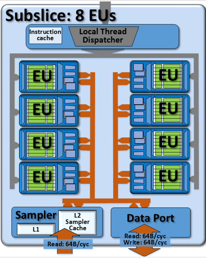
The Intel processor graphics gen9 subslice, containing 8 EUs each. The subslice also instantiates sampler and data port units per subslice
英特尔处理器图形gen9子切片,每个包含8个EU。 该子切片还实例化每个子切片的采样器和数据端口单元
5.4 SUBSLICE ARCHITECTURE
In gen9 compute architecture, arrays of EUs are instantiated in a group called a subslice. For scalability, product architects can choose the number of EUs per subslice. For most gen9-based products, each subslice contains 8 EUs. Each subslice contains its own local thread.
在gen9计算架构中,EU阵列在称为子切片的组中实例化。 为了实现可伸缩性,产品架构师可以选择每个子切片的EU数。 对于大多数基于gen9的产品,每个子切片包含8个EU。 每个子切片包含其自己的本地线程。
dispatcher unit and its own supporting instruction caches. Given these 8 EUs with 7 threads each, a single subslice has dedicated hardware resources and register files for a total of 56 simultaneous threads. Each subslice also includes a sampler unit and a data port memory management unit. Compared to the Gen7.5 design which had 10 EUs per subslice, the gen8 and gen9 designs reduce the number EUs sharing each subslice’s sampler and data port. From the viewpoint of each EU, this has the effect of improving effective bandwidth local to the subslice.
dispatcher 调度程序单元及其自身支持的指令缓存。 假设这8个EU每个都有7个线程,则单个子切片具有专用的硬件资源和寄存器文件,总共56个并发线程。 每个子切片还包括一个采样器单元和一个数据端口内存管理单元。 相比Gen7.5的每个子切片有10个EU,gen8和gen9设计减少了共享每个子切片的采样器和数据端口的EU数量。 从每个EU的角度来看,这有助于改善子切片本地有效带宽的作用。
5.4.1 Sampler
The sampler is a read-only memory fetch unit that may be used for sampling of tiled (or not tiled) texture and image surfaces. The sampler includes a level-1 sampler cache (L1) and a level-2 sampler cache (L2). Between the two caches is dedicated logic to support dynamic decompression of block compression texture formats such as DirectX BC1-BC7, DXT, and OpenGL compressed texture formats. The sampler also includes fixed-function logic that enables address conversion on image (u,v) coordinates, and address clamping modes such as mirror, wrap, border, and clamp. Finally, the sampler supports a variety of sampling filtering modes such as point, bilinear, tri-linear, and anisotropic.
采样器是一个只读存储器获取单元,可用于对平铺(或非平铺)纹理和图像表面进行采样。 采样器包括一个1级采样器缓存(L1)和一个2级采样器缓存(L2)。 在这两个缓存之间是专用逻辑,用于支持块压缩纹理格式(例如DirectX BC1-BC7,DXT和OpenGL压缩纹理格式)的动态解压缩。 采样器还包括固定功能逻辑,可在图像(u,v)坐标上进行地址转换,并提供地址钳位模式,例如镜像,环绕,边界和钳位。 最后,采样器支持各种采样滤波模式,例如点采样,双线性采样,三线性采样和各向异性采样。
5.4.2 Data Port
Each subslice also contains a memory load/store unit called the data port. The data port supports efficient read/write operations for a variety of general purpose buffer accesses, flexible SIMD scatter/gather operations, as well as shared local memory access. To maximize memory bandwidth, the unit dynamically coalesces scattered memory operations into fewer operations over non-duplicated 64-byte cacheline requests. For example, a SIMD-16 gather operation against 16 unique offset addresses for 16 32-bit floating-point values, might be coalesced to a single 64-byte read operation if all the addresses fall within a single cacheline.
每个子切片还包含一个称为数据端口的内存加载/存储单元。 数据端口提供用于访问各种通用缓冲区的高效读/写操作操作,灵活的SIMD分散/收集操作以及共享本地内存的访问。 为了最大程度地提高内存带宽,该单元通过非重复的64字节高速缓存行请求,将分散的内存操作动态合并为更少的操作。 例如,针对16个32位浮点值的16个唯一偏移地址,如果所有地址都落在单个缓存行内, SIMD-16收集操作,则可能会合并为单个64字节读取操作。
5.5 SLICE ARCHITECTURE
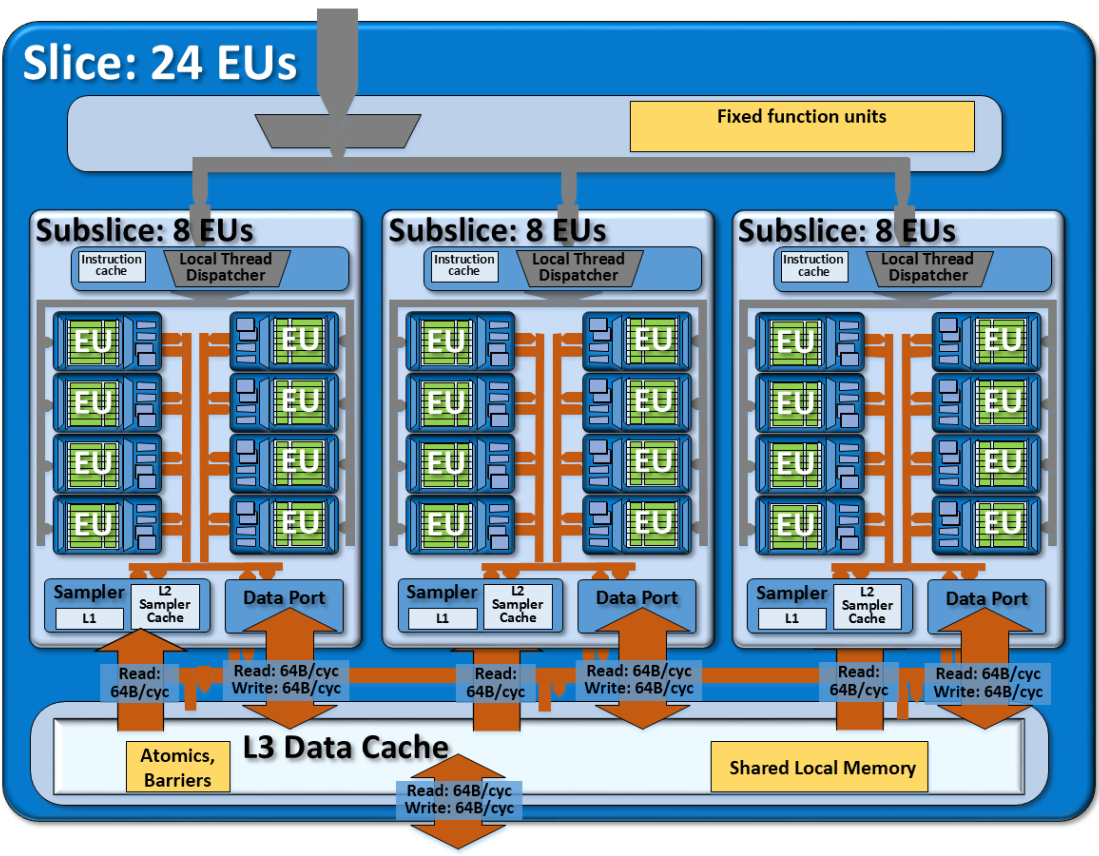
The Intel processor graphics gen9 slice, containing three subslices for a total of 24 EUs. The slice adds supporting L3 cache, shared local memory, atomics, barriers, and other fixed function units.
英特尔处理器图形gen9切片,包含三个子切片,总计24个EU。 该片添加了支持的L3高速缓存,共享的本地内存,原子,屏障和其他固定功能单元。
Subslices are clustered into slices. For most gen9-based products, 3 subslices are aggregated into 1 slice. Thus a single slice aggregates a total of 24 EUs[3]. Aside from grouping subslices, the slice integrates additional logic for thread dispatch routing, a banked level-3 cache, a smaller but highly banked shared local memory structure, and fixed function logic for atomics and barriers. Additional fixed function units support the media and graphics capability, but are not discussed here.
子切片聚集成切片。 对于大多数基于gen9的产品,将3个子切片聚合为1个切片。 因此,单个切片总共有24个EU [3]。 除了对子分片进行分组之外,分片还集成了用于线程调度路由的其他逻辑,存储(banked)3级缓存,更小但存储量很高的共享本地内存结构以及用于原子和屏障的固定功能逻辑。 附加的固定功能单元支持媒体和图形功能,但此处不再讨论。
[3] Note some gen9-based products may enable fewer than 24 EUs in a slice.
5.5.1 Level-3 Data Cache
For gen9-based products, the level-3 (L3) data cache capacity has been increased to 768Kbytes total per slice. Each application context has flexibility as to how much of the L3 memory structure is allocated: 1) as application L3 data cache, 2) as system buffers for fixedfunction pipelines, and 3) as shared local memory. For example, 3D rendering contexts often allocate more L3 as system buffers to support their fixed-function pipelines, instead of as shared local memory. For compute application contexts on gen9 compute architecture, the typical allocation is 512 Kbytes per slice as application data cache.
对于基于Gen9的产品,三级(L3)数据高速缓存容量已增加到每个切片总计768KB。 每个应用程序上下文对于分配多少L3内存结构具有灵活性:1)作为应用程序L3数据高速缓存,2)作为固定功能管道的系统缓冲区,以及3)作为共享本地内存。 例如,3D渲染上下文通常将更多的L3分配为系统缓冲区以支持其固定功能管道,而不是作为共享本地内存。 对于gen9计算架构上的计算应用程序上下文,每个slice分片,典型的分配512 KB作为应用程序数据缓存。
As with previous generations, gen9 products with multiple subslices will instantiate multiple L3 cache partitions. These cache partitions aggregate together via an L3 fabric and act as a single larger capacity monolithic cache. This L3 fabric is also expandable across multiple slices for even larger cache aggregations. Cachelines are 64 bytes each, and they are uniformly distributed across the entire aggregate cache.
与前几代产品一样,具有多个子切片的gen9产品将实例化多个L3缓存分区。 这些缓存分区通过L3架构聚合在一起,并充当单个更大容量的单片缓存。 该L3结构还可以跨多个slice扩展,以实现更大的缓存聚合。 高速缓存行每个为64字节,它们均匀地分布在整个聚合高速缓存中。
All samplers and data ports are given their own separate memory interface to the L3. The interface between each data port and the L3 data cache enables both read and write of 64 bytes per cycle. Thus a slice containing three subslices, each with a unique data port, will have an aggregate L3 bandwidth of 192 bytes per cycle. For accesses that miss the L3 cache, the L3 fill logic can read and write system memory data at 64 bytes per cycle.
所有采样器和数据端口都为L3分配了独立的存储器接口。 每个数据端口和L3数据高速缓存之间的接口使每个周期可以读取和写入64个字节。 因此,包含三个子切片(每个切片具有唯一的数据端口)的切片将具有每个周期192字节的L3聚合带宽。 对于缺少L3高速缓存的访问,L3填充逻辑可以每个周期以64字节读取和写入系统内存数据。
All data in and out of the samplers and data ports flows through the L3 data cache in units of 64-byte-wide cachelines. This includes read and write actions on general purpose buffers. It also includes sampler read transactions that miss the level-1 (L1) and level-2 (L2) sampler caches. L3 cache bandwidth efficiency is highest for read/write accesses that are cacheline-aligned and adjacent within a cacheline. Compute kernel instructions that miss the subslice instruction caches flow through the L3 cache.
所有进出采样器和数据端口的数据都以64字节宽的缓存行为单位流经L3数据缓存。 这包括对通用缓冲区的读取和写入操作。 它还包括错过一级(L1)和二级(L2)采样器高速缓存的采样器读取事务。 对于高速缓存行对齐且在高速缓存行内相邻的读/写访问,L3高速缓存带宽效率最高。 没用命中子切片指令缓存的计算内核指令将流经L3缓存。
5.5.2 Shared Local Memory
Shared local memory[4] is a structure within the L3 complex that supports programmermanaged data for sharing among EU hardware threads within the same subslice. The read/write bus interface between each subslice and shared local memory is again 64-bytes wide. Latency wise, access to shared local memory is similar to accessing the L3 data cache. However, the shared local memory itself is more highly banked than the L3 data cache. The shared local memory banking can yield full shared local memory bandwidth for access patterns that may not be 64-byte aligned or that may not be contiguously adjacent in memory. For gen9-based products, 64 Kbytes of shared local memory are dedicated and available per subslice. Note that shared local memory is not coherent with other memory structures.
共享本地内存[4]是L3组合系统中的一种结构,它支持程序员管理的数据,以便在同一子切片内的EU硬件线程之间共享。 每个子切片和共享本地内存之间的读/写总线接口也是64字节宽。 在延迟方面,访问共享本地内存类似于访问L3数据缓存。 但是,共享本地内存本身比L3数据高速缓存具有更高的banked。 共享的本地内存存储区可以为可能不是64字节对齐的或在内存中不相邻的访问模式提供完整的共享本地内存带宽。 对于基于gen9的产品,每个子切片专用于64 KB的共享本地内存。 请注意,共享本地内存与其他内存结构不一致。
banked:
收集或形成一个团块,球状,围成一排。
SPMD programming model constructs such as OpenCL’s local memory space or DirectX Compute Shader’s shared memory space are shared across a single work-group (threadgroup). For software kernel instances that use shared local memory, driver runtimes typically map all instances within a given OpenCL work-group (or a DirectX 11 threadgroup) to EU threads within a single subslice. Thus all kernel instances within a work-group will share access to the same 64 Kbyte shared local memory partition. Because of this property, an application’s accesses to shared local memory should scale with the number of subslices.
SPMD编程模型构造(例如OpenCL的本地内存空间或DirectX Compute Shader的共享内存空间)在单个工作组(线程组)之间共享。 对于使用共享本地内存的软件内核实例,驱动程序运行时通常会将给定OpenCL工作组(或DirectX 11线程组)中的所有实例映射到单个子切片中的EU线程。 因此,工作组中的所有内核实例将共享对同一64 KB共享本地内存分区的访问。 由于具有此属性,因此应用程序对共享本地内存的访问应随子切片数的增加而扩展。
[4] We use the term shared local memory to indicate the hardware memory structure that supports the software address space (OpenCL refers to it as work-group local memory, and which DirectX Compute Shader refers to as thread-group shared memory).
[4]我们使用共享本地内存一词来表示支持软件地址空间的硬件内存结构(OpenCL将其称为工作组本地内存,而DirectX Compute Shader将其称为线程组共享内存)。
5.5.3 Barriers and Atomics
Each slice within gen9 compute architecture bundles dedicated logic to support implementation of barriers across groups of threads. This barrier logic is available as a hardware alternative to pure compiler-based barrier implementation approaches. The gen9 logic can support barriers simultaneously in up to 16 active thread-groups per subslice.
gen9计算体系结构中的每个切片捆绑了专用逻辑,以支持跨线程组实现屏障。 此屏障逻辑可作为纯基于编译器的屏障实现方法的硬件替代品。 gen9逻辑可以在每个子切片最多16个活动线程组中同时支持屏障。
Each slice also provides a rich suite of atomic read-modify-write memory operations. These operations support both operations to L3 cached global memory or to shared local memory. Gen9-based products support 32-bit atomic operations.
每个切片还提供了丰富的原子读-修改-写存储器操作套件。 这些操作支持对L3缓存的全局内存或共享本地内存的两种操作。 基于Gen9的产品支持32位原子操作。
5.5.4 64-Byte Data Width
A foundational element of gen9 compute architecture is the 64-byte data width. Recall that each EU thread’s register file is composed of 128 32-byte registers (SIMD-8 x 32-bit). But recall also that operands to SIMD-16 instructions typically pair two such registers, treating the pair as a single 64-byte SIMD-16 register. Observe:
A SIMD-16 instruction can source 64-byte wide operands from 64-byte wide registers.
The data for such 64-byte wide registers are read and written from L3 over a 64-byte wide data bus.
Within the L3 data cache, each cacheline is again 64-bytes wide.
Finally the L3 cache’s bus interface to the SoC-shared LLC is also 64-bytes wide.
gen9计算体系结构的基本要素是64字节数据宽度。 回想一下,每个EU线程的寄存器文件都由128个32字节寄存器(SIMD-8 x 32位)组成。 但是还要记住,SIMD-16指令的操作数通常将两个这样的寄存器配对,将这对视为单个64字节的SIMD-16寄存器。 观察:
SIMD-16指令可以从64字节宽的寄存器中获取64字节宽的操作数。
通过64字节宽的数据总线从L3读取和写入此类64字节宽的寄存器的数据。
在L3数据高速缓存中,每条高速缓存行又是64字节宽。
最后,L3缓存与SoC共享LLC的总线接口也为64字节宽。
5.6 PRODUCT ARCHITECTURE
Finally, SoC product architects can create product families or a specific product within a family by instantiating a single slice or groups of slices. Members of a product family might differ primarily in the number of slices. These slices are combined with additional front end logic to manage command submission, as well as fixed-function logic to support 3D, rendering, and media pipelines. Additionally the entire gen9 compute architecture interfaces to the rest of the SoC components via a dedicated unit called the graphics technology interface (GTI)
最后,SoC产品架构师可以通过实例化单个切片或片组来创建产品系列或系列中的特定产品。 产品系列的成员可能主要不同之处在于切片的数量。 这些切片与其他前端逻辑(用于管理命令提交)以及固定功能逻辑(用于支持3D,渲染和媒体管道)结合在一起。 此外,整个gen9计算架构还通过称为图形技术接口(GTI)的专用单元与其余SoC组件接口。
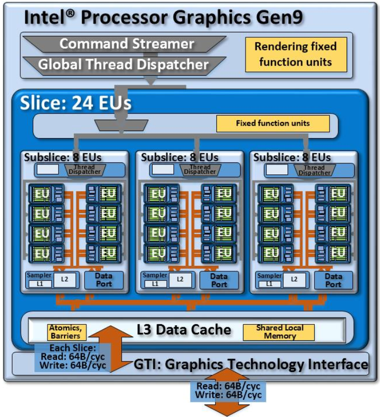
A potential product design that instantiates the compute architecture of Intel® processor graphics gen9. It is composed of a single slice with three subslices, for a total of 24 EUs. The Intel® Core™ i7 processor 6700K with Intel® HD Graphics 530 instantiates such a design
潜在产品设计可实例化Intel®处理器图形gen9的计算架构。 它由一个带有三个子切片的单个切片组成,总共有24个EU。 带有英特尔®HD Graphics 530的英特尔®酷睿™i7处理器6700K实例化了这种设计
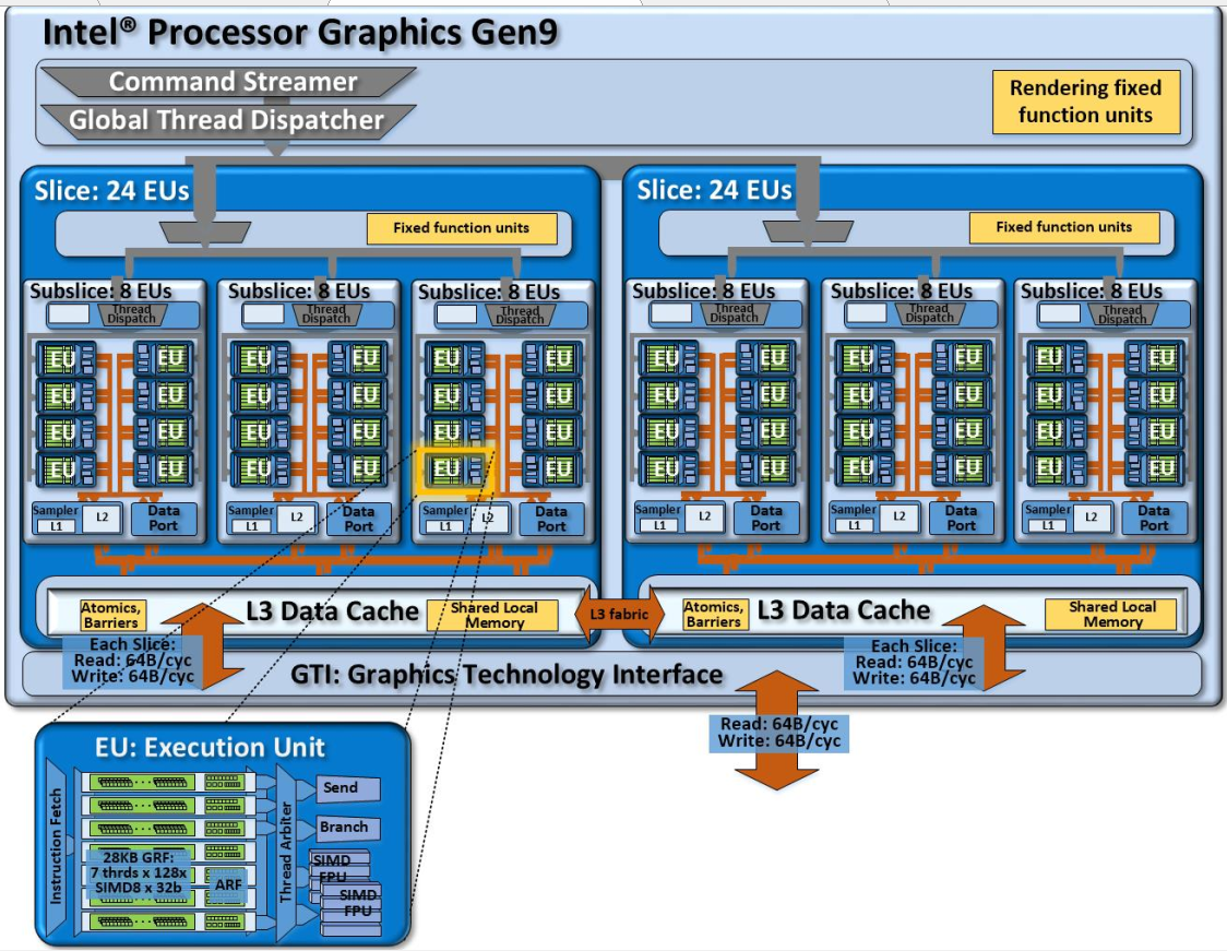
Another potential product design that instantiates the compute architecture of Intel® processor graphics gen9. This design is composed of two slices, of three subslices each for a total of 48 EUs
另一个可能的产品设计实例化了英特尔®处理器图形gen9的计算架构。 此设计由两部分组成,每部分三个子切片,总共48个EU
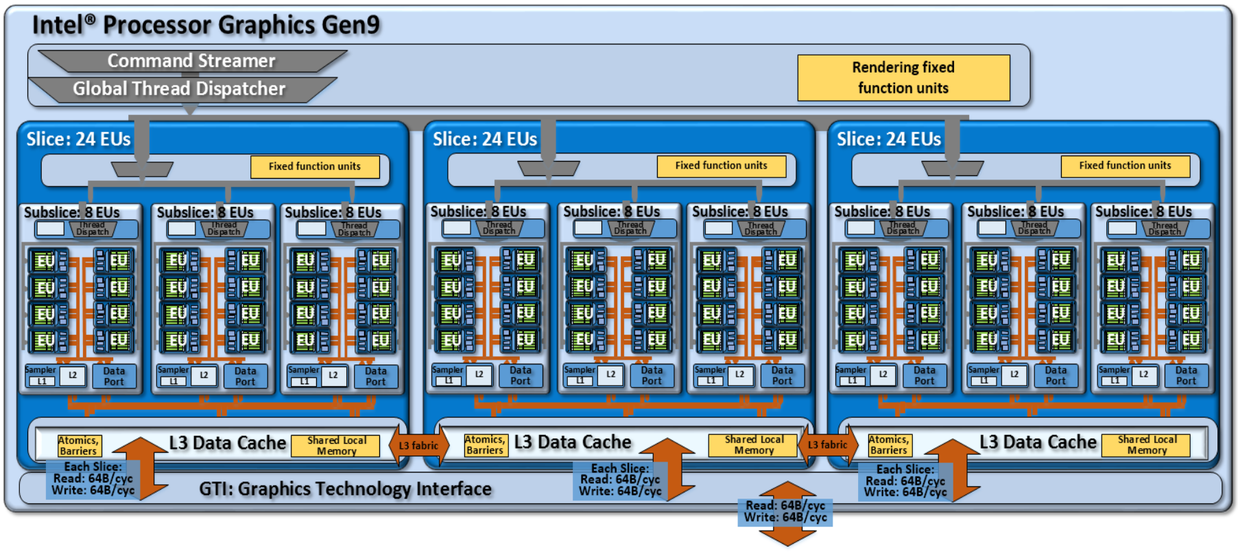
Another potential product design that instantiates the compute architecture of Intel® processor graphics gen9. This design is composed of three slices, of three subslices each for a total of 72 EUs
另一个可能的产品设计实例化了英特尔®处理器图形gen9的计算架构。 此设计由三层组成,每层三个子切片,总共72个EU
5.6.1 Command Streamer and Global Thread Dispatcher
As its name implies, the command streamer efficiently parses command streams submitted from driver stacks and routes individual commands to their representative units. For compute workloads, the global thread dispatcher is responsible for load balancing thread distribution across the entire device. The global thread dispatcher works in concert with local thread dispatchers in each subslice.
顾名思义,命令流传输器有效地解析从驱动程序堆栈提交的命令流,并将单个命令路由到其代表单元。 对于计算工作负载,全局线程分派器负责负载平衡整个设备上的线程。 全局线程分派器与每个子切片中的本地线程分派器协同工作。
The global thread dispatcher operates in two modes. For compute workloads that do not depend on hardware barriers or on shared local memory, the global thread dispatcher may distribute the workload over all available subslices to maximize throughput and utilization. Given the unit’s global visibility, it is able to load balance across all the execution resources. For compute workloads that do depend upon hardware barriers or shared local memory, the global thread dispatcher will assign thread-group sized portions of the workload to specific subslices. Such an assignment ensures localized access to the barrier logic and shared local memory storage dedicated to each subslice.
全局线程分派器以两种模式运行。 对于不依赖于硬件屏障或共享本地内存的计算工作负载,全局线程分派器可以将工作负载分布在所有可用子切片上,以最大化吞吐量和利用率。 鉴于单元的全局可见性,它能够在所有执行资源之间实现负载平衡。 对于确实依赖于硬件屏障或共享本地内存的计算工作负载,全局线程分派器会将工作负载的线程组大小部分分配给特定的子切片。 这样的分配确保对屏障逻辑的本地访问和专用于每个子切片的共享本地内存存储。
5.6.2 Graphics Technology Interface (GTI)
The graphics technology interface, or GTI, is the gateway between gen9 compute architecture with the rest of the SoC. The rest of the SoC includes memory hierarchy elements such as the shared LLC memory, the system DRAM, and possibly embedded DRAM. GTI facilitates communication with the CPU cores and possibly with other fixed function devices such as camera imaging pipelines. GTI also implements global memory atomics that may be shared between Intel processor graphics gen9 and CPU cores. Finally GTI implements power management controls for Intel processor graphics gen9 and interfaces between the GTI clock domain and the (usually different) SoC clock domains.
图形技术接口或GTI是gen9计算架构与SoC其余部分之间的网关。 SoC的其余部分包括内存层次结构元素,例如共享LLC内存,系统DRAM以及可能的嵌入式DRAM。 GTI促进了与CPU内核以及可能与其他固定功能设备(例如相机成像管线)的通信。 GTI还实现了可以在Intel处理器gen9和CPU内核之间共享的全局内存原子。 最后,GTI对Intel处理器图形Gen9以及GTI时钟域和(通常是不同的)SoC时钟域之间的接口实施电源管理控件。
The bus between each slice that is interfaced to GTI is capable of 64-bytes per cycle read and 64-bytes per cycle write. Internally, GTI has memory request queues to maintain memory order and manage differing latencies on individual memory requests. For instances of Intel processor graphics gen9, the bus between GTI and LLC has two possible configurations. Like gen8, higher-performance gen9 configurations are capable of 64-bytes per cycle read and 64-bytes per cycle write. A second configuration for lower power is capable of 64-bytes per cycle read and 32-bytes per cycle write. Like other aspects of the architecture, this bus width is also scalable, and SoC designers may configure it for specific products.
连接到GTI的每个片之间的总线能够读取每个周期64个字节,写入每个周期64个字节。 在内部,GTI具有内存请求队列以维护内存顺序并管理各个内存请求的不同延迟。 对于第9代英特尔处理器图形,GTI和LLC之间的总线有两种可能的配置。 与gen8一样,性能更高的gen9配置能够在每个周期读取64字节,在每个周期写入64字节。 降低功耗的第二种配置是每个周期读取64字节,每个周期写入32字节。 像架构的其他方面一样,此总线宽度也是可扩展的,SoC设计人员可以为特定产品配置它。
5.6.3 Unslice
The command streamer, global thread dispatcher, and graphics technology interface all exist independent of the slice instantiations, in a domain typically called the “unslice.” New to gen9, this domain is given its own power gating and clocking that can run at the same or faster than the slice clock. This can enable intelligent power savings by dynamically diverting more power to GTI’s memory bandwidth, versus the EU slices’s compute capability. This can be particularly effective for low power media playback modes.
命令流,全局线程分派器和图形技术接口都独立于切片实例化而存在,通常在一个称为“ unslice”的域中。对于gen9来说,此域具有自己的电源门控和时钟,可以在同一时间运行 或比切片时钟快。 通过动态地将更多的功率分配给GTI的内存带宽(与EU Slice的计算能力相比),可以实现智能节能。 这对于低功耗媒体播放模式可能特别有效。
5.6.4 Product EU Counts
Although gen9 subslices generally contain 8 EUs each, complete gen9-based products can disable an EU within a subslice to optimize product yields from silicon manufacturing. For example, a three subslice-based product can have a total of 23 EUs by disabling an EU in one subslice.
尽管gen9子切片通常每个都包含8个EU,但是完整的基于gen9的产品可以禁用子切片中的EU,以优化硅制造的产品产量。 例如,一个基于三个子切片的产品通过在一个子切边中禁用一个EU可以总共具有23个EU。
5.7 MEMORY
5.7.1 Unified Memory Architecture
Intel processor graphics architecture has long pioneered sharing DRAM physical memory with the CPU. This unified memory architecture offers a number of system design, power efficiency, and programmability advantages over PCI Express-hosted discrete memory systems.
英特尔处理器图形架构长期以来一直是与CPU共享DRAM物理内存的先驱。 与PCI Express托管的离散内存系统相比,这种统一的内存体系结构提供了许多系统设计,能效和可编程性方面的优势。
The obvious advantage is that shared physical memory enables zero copy buffer transfers between CPUs and gen9 compute architecture. By zero copy, we mean that no buffer copy is necessary since the physical memory is shared. Moreover, the architecture further augments the performance of such memory sharing with a shared LLC cache. The net effect of this architecture benefits performance, conserves memory footprint, and indirectly conserves system power not spent needlessly copying data. Shared physical memory and zero copy buffer transfers are programmable through the buffer allocation mechanisms in APIs such as OpenCL 1.0+ and DirectX11.2+.
明显的优势在于,共享的物理内存可实现CPU与gen9计算架构之间的零复制缓冲区传输。 零拷贝意味着没有缓冲拷贝是必需的,因为物理内存是共享的。 此外,该架构还通过共享的LLC缓存来增强这种内存共享的性能。 这种架构的最终效果是提高了性能,节省了内存占用空间,并间接节省了不必要地花费在复制数据上的系统功能。 共享的物理内存和零复制缓冲区传输可通过API(例如OpenCL 1.0+和DirectX11.2 +)中的缓冲区分配机制进行编程。
5.7.2 Shared Memory Coherency
Gen9 compute architecture supports global memory coherency between Intel processorgraphics and the CPU cores. SoC products with Intel processor graphics gen9 integrate newhardware components to support the recently updated Intel® Virtualization Technology (Intel®VT) for Directed I/O (Intel® VT-d) specification. This specification extends Intel VT, whichgenerally addresses virtual machine to physical machine usage models and enables virtualmachine monitor implementation. In particular, the recent Intel VT-d specification extensionsdefine new page table entry formats, cache protocols, and hardware snooping mechanisms forshared memory between CPU cores and devices such as Intel processor graphics.
Gen9计算架构支持Intel处理器图形和CPU内核之间的全局内存一致性。 具有Intel处理器图形第9代的SoC产品集成了新的硬件组件,以支持最近更新的针对定向I / O的英特尔®虚拟化技术(Intel®VT)(Intel®VT-d)规范。 该规范扩展了Intel VT,后者通常将虚拟机处理为物理机使用模型,并支持虚拟机监控器的实现。 特别是,最近的Intel VT-d规范扩展定义了新的页表条目格式,高速缓存协议和硬件侦听机制,用于CPU内核与设备(例如Intel处理器图形)之间的共享内存。
These new mechanisms can be used to maintain memory coherency and consistency for fine grained sharing throughout the memory hierarchy between CPU cores and devices. Moreover, the same virtual addresses can be shared seamlessly across devices. Such memory sharing is application-programmable through emerging heterogeneous compute APIs such as the shared virtual memory (SVM) features specified in OpenCL 2.0. The net effect is that pointer-rich datastructures can be shared directly between application code running on CPU cores with application code running on Intel processor graphics, without programmer data structure marshalling or cumbersome software translation techniques.
这些新机制可用于维护内存一致性和一致性,以便在CPU内核和设备之间的整个内存层次结构中实现细粒度的共享。 此外,可以在设备之间无缝共享相同的虚拟地址。 这样的内存共享可以通过新兴的异构计算API(例如OpenCL 2.0中指定的共享虚拟内存(SVM)功能)进行应用程序编程。 最终结果是,可以在运行于CPU内核上的应用程序代码与运行于Intel处理器图形上的应用程序代码之间直接共享富指针数据结构,而无需编组数据结构或使用繁琐的软件转换技术。
Within Intel processor graphics, the data port unit, L3 data cache, and GTI have all been upgraded to support a new globally coherent memory type. Reads and writes originating from Intel processor graphics to memory typed as globally coherent and drive Intel VT-d-specified snooping protocols to ensure data integrity with any CPU core cached versions of that memory. Conversely, the same is true for GPU cached memory and reads ands writes that originate from the CPU cores. The coherent memory hierarchy is shown in Figure 9. Note that the sampler’s L1 and L2 caches as well as the shared local memory structures are not coherent.
在Intel处理器图形中,数据端口单元,L3数据缓存和GTI均已升级,以支持新的全局一致性内存类型。 读取和写入源自Intel处理器图形的内存,并将其写入类型为全局一致的内存,并驱动Intel VT-d指定的侦听协议,以确保该内存的任何CPU内核缓存版本均具有数据完整性。 相反,GPU缓存内存以及源自CPU内核的读写操作也是如此。 一致性存储器层次结构如图9所示。请注意,采样器的L1和L2缓存以及共享的本地存储器结构不是一致性的。
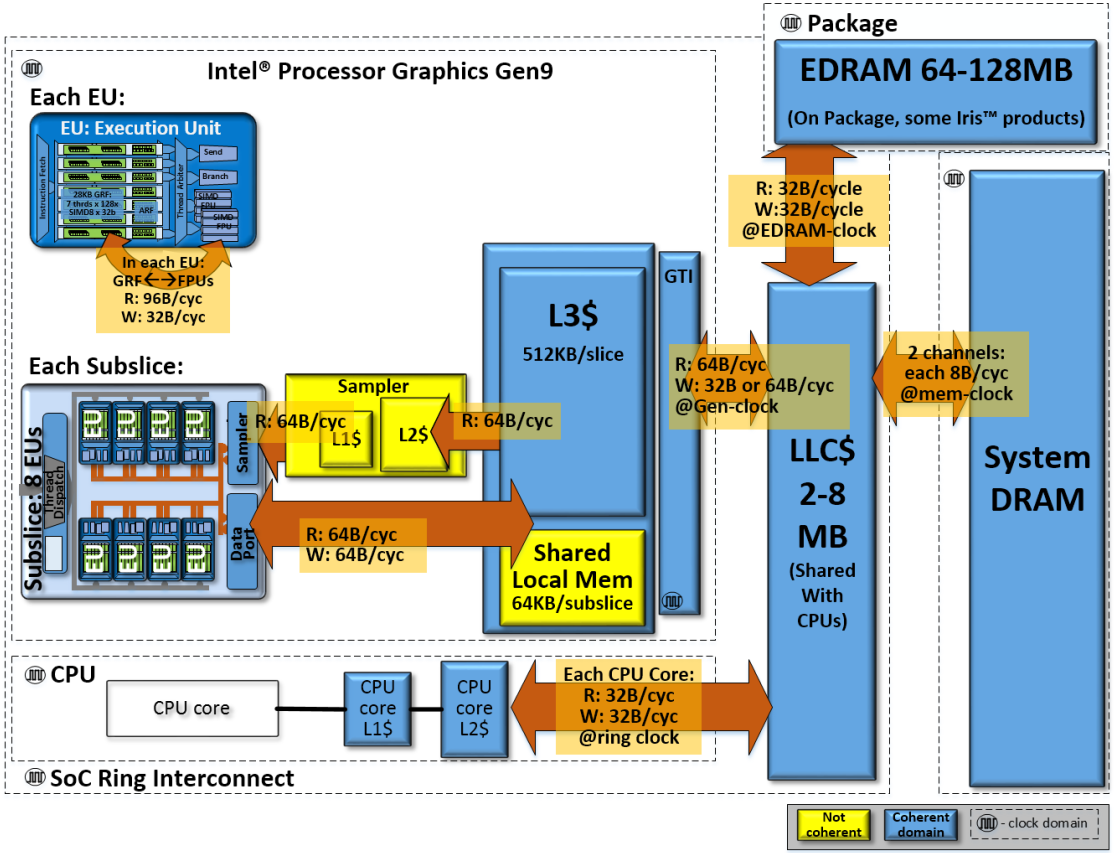
Figure 9: A view of the SoC chip level memory hierarchy and its theoretical peak bandwidths for the compute architecture of Intel processor graphics gen9.
图9:SoC芯片级内存层次结构及其理论峰值带宽的视图,用于Intel处理器图形gen9的计算架构。
【REF】
clamp 钳位
[0075] BNewt x=CLAMP (Bk,!+GrayNewkj x-Graykj 1; 0, 255)
[0076] 其中,RNewtl为转换后的红色通道值,GNewtl转换后的绿色通道值,BNewtl为转换后的蓝色通道值,Riu为原图像的红色通道值,Giu原图像的绿色通道值,Biu为原图像的蓝色通道值;GrayNeWlu为第二灰度值,Grayiu为第一灰度值;CLAMP (a, b, c)函数表示,取a, b,c之中中间大小的值,k为人脸皮肤区域内横轴像素点个数和I人脸皮肤区域内纵轴像素点个数。
clamp表示夹紧,夹住的意思,torch.clamp(input,min,max,out=None)-> Tensor
将input中的元素限制在[min,max]范围内并返回一个Tensor

 浙公网安备 33010602011771号