LPC43xx SGPIO I2C Implementation

I²C SGPIO Configuration
SGPIO is a hardware feature of LPC4300 series.
There are 16 SGPIO pins called from SGPIO 0 to SGPIO 15.
SGPIO is one of the functions of LPC 4300 pins which can be chosen.
SGPIO could work as standard GPIO pins, or do stream processing.
So it provides a number of possibilities for interface implementation.
Each pin of SGPIO has a configuration as shown in Figure 1-7 .
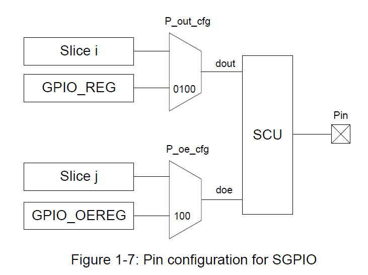
The pin function has been chosen by SCU (System Control Unit) as SGPIO function.
What left should be configured with SGPIO pin is set by bits of OUT_MUX_CFG Register.
OUT_MUX_CFG consists of two parts, P_out_cfg and P_oe_cfg.
P_out_cfg decides whether a slice or GPIO_REG generates the output signal (dout).
P_oe_cfg selects whether slice or GPIO_OEREG to be output enable (doe).
All the relevant SGPIO registers information is in Appendix B.
Slice is an enhanced feature of SGPIO to accelerate serial streaming.
The construction of one slice is in Figure 1-8.
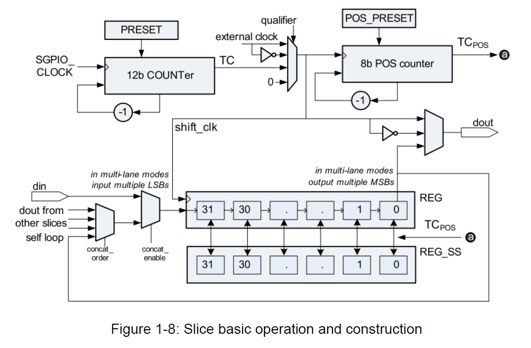
REG register is a shift register to generate output or get input for one slice.
REG_SS is the slice data shadow register.
POS register is a down counter.
The first 8 bits (POS_COUNTER) of POS register indicates the current number of shifts left before the exchange between REG and REG_SS.
The last 8 bits (POS_PRESET) of POS register sets the reload value of POS_COUNTER.
REG and REG_SS will exchange the content when the down counter POS_COUNTER reaches 0x0.
This feature can be used to change new output value of on slice.
PRESET register sets the reload value of the counter, in other words, it controls the rate of shift clock.
COUNT register reflects the slice clock counter value.
When COUNT equals 0x0, POS_COUNTER counts down, and REG shifts once.
All the details about setting of one slice are in section 5.4.
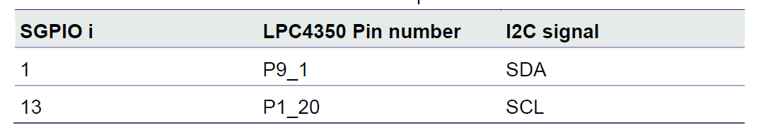
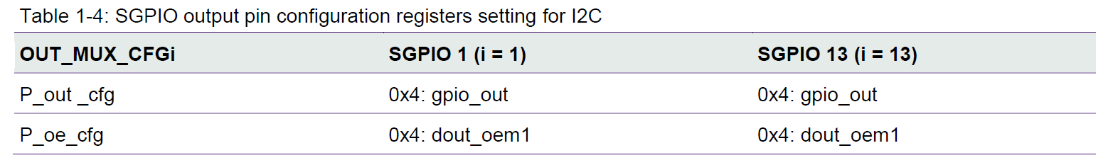
To configure LPC4350 pins to be I2C signal pins, two SGPIO pins should be chosen first.
In this demo, SGPIO 1 and SGPIO 13 are defined as SDA and SCL respectively.
With looking up the table in section 6.2 (Pin description) of LPC4350 datasheet (6),
the available pins to be SGPIO 1 and SGPIO 13 could be found.
Possible pins for SGPIO 1 are P0_1, P9_1, and PF_2.
Possible pins for SGPIO 13 are P1_20, P2_4, P4_8, PC_14, and PD_9.
Not all the pins in the list above are available to use on the real board.
In order to choose the proper pins from them, the schematics of the evaluation board has been consulted.
The requirements to define free pins on the board are as follows,
It should have a jumper between the pin of LPC4350 and a certain chip or circuit.
The signal of SDA or SCL will not affect the previous function of the pin.
According to these requirements, the choices left for SGPIO 1 are P0_1, P9_1, and PF_2.
For SGPIO 13, the pins meet the requirements are P1_20, P2_4, P4_8.
Finally, P9_1 and P1_20 are picked. The overall information of selected LPC4350 pins is in Table 1-1.
Table 1-1: I2C function and SGPIO number of selected LPC4350 pins
The System Control Unit (SCU)/ IO configuration should be set for each pin.
The pin configuration registers bit description is in page 227 of LPC4350 user manual, which is also in Appendix C Table C-1.
What should be set in pin configuration register are
pin function, pull-up enable, pull-down enable, slew rate, input buffer enable and input glitch filter.
As for pin function, both of P9_1 and P1_20 work in SGPIO mode numbered as function 6.
For I2C Standard-mode, the signal rates are below 30 MHz, so the pins should be set as slow rate and input glitch filter enable.
The pins are set as pull-up enable due to the construction of I2C masters and slaves (see next paragraph).
Input buffer is enabled to make SGPIO streaming possible.
As to create a suitable SGPIO configuration for I2C protocol, first should look into the construction
both master side and slave side (see Figure 1-10).
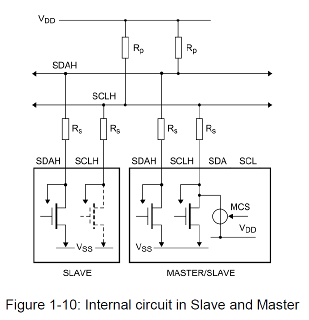
The SDA line is originally high with the pull up, so SGPIO could not always drive it high.
An example can explain this in Figure 1-9.
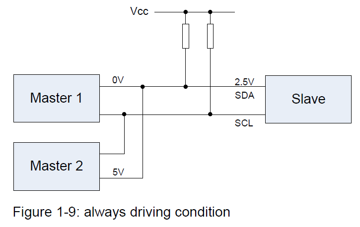
If master 2 is always driving SDA line, assume the voltage on master 2 is 5 V and master 1 now wants to transfer data and drive SDA line low.
In this situation, the final voltage on SDA line is 2.5V. In conclusion, what should be done is to drive SDA low when there’s a need.
The condition is exactly the same for SCL line.
The setting of SGPIO pin configuration is in Figure 1-11.
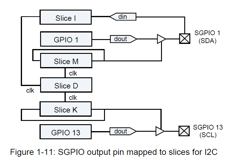
For SGPIO 1, the SDA line, GPIO mode is to generate output, and output value is set by GPIO_OUTREG register.
Slice M is output enable as a driver.
Slice M is in a self-loop.
Slice I gets the input from SGPIO 1 during I2C data receiving.
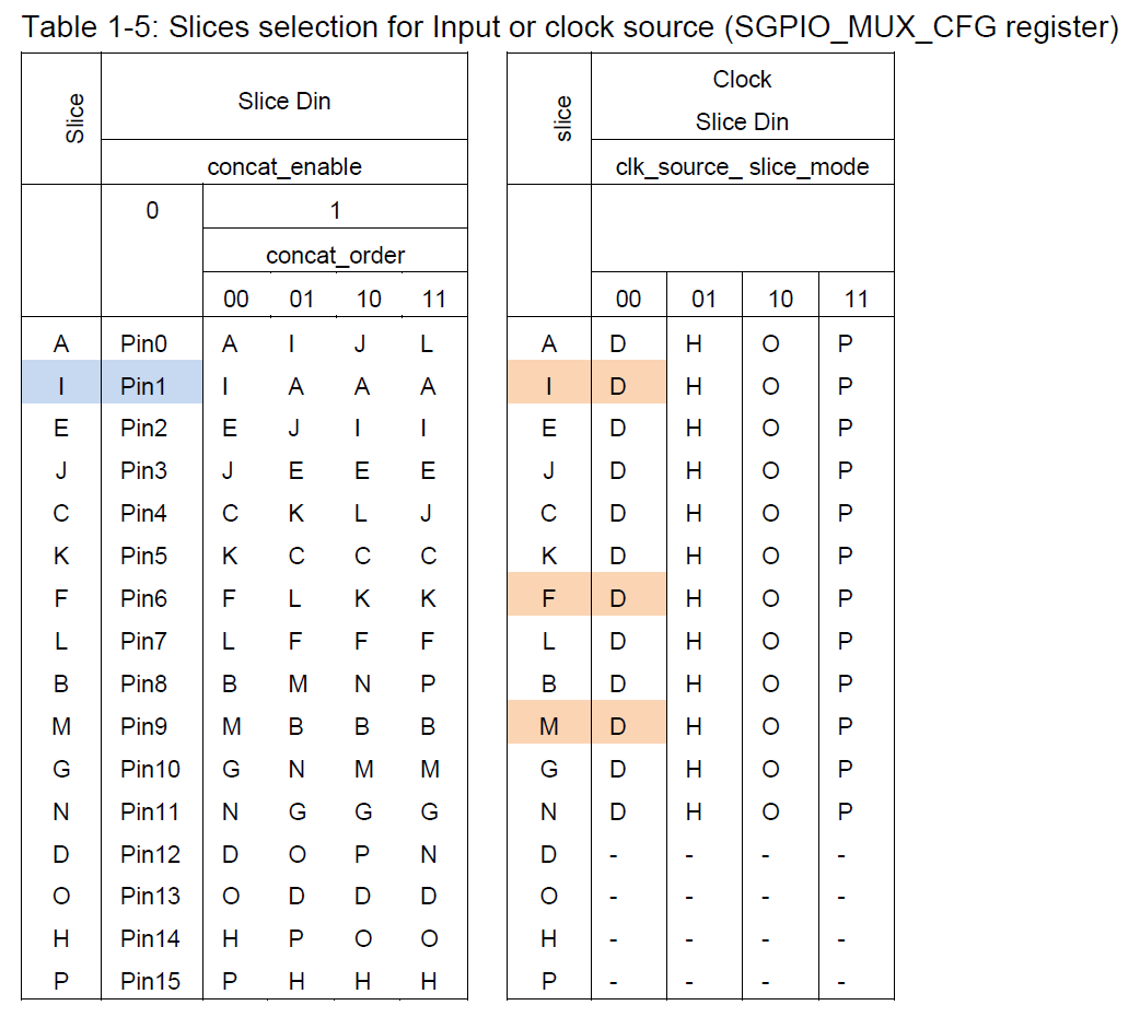
The way to choose Slice I as input is according to Table 1-5 in section 5.4.
In terms of SGPIO 13, GPIO mode is to generate output.
Slice K is self-looped and set to be output enable.
Slice D is the clock source for Slice I, M, and K.
To find the way to select clock source for each slice, please refer to Table 1-5 in section 5.4.
The selection of slices that are related to output mode is according to the Table 1-2 and Table 1-3.
The blue blocks represent slices mapping of SGPIO 1.
The green blocks indicate slices mapping of SGPIO 13.
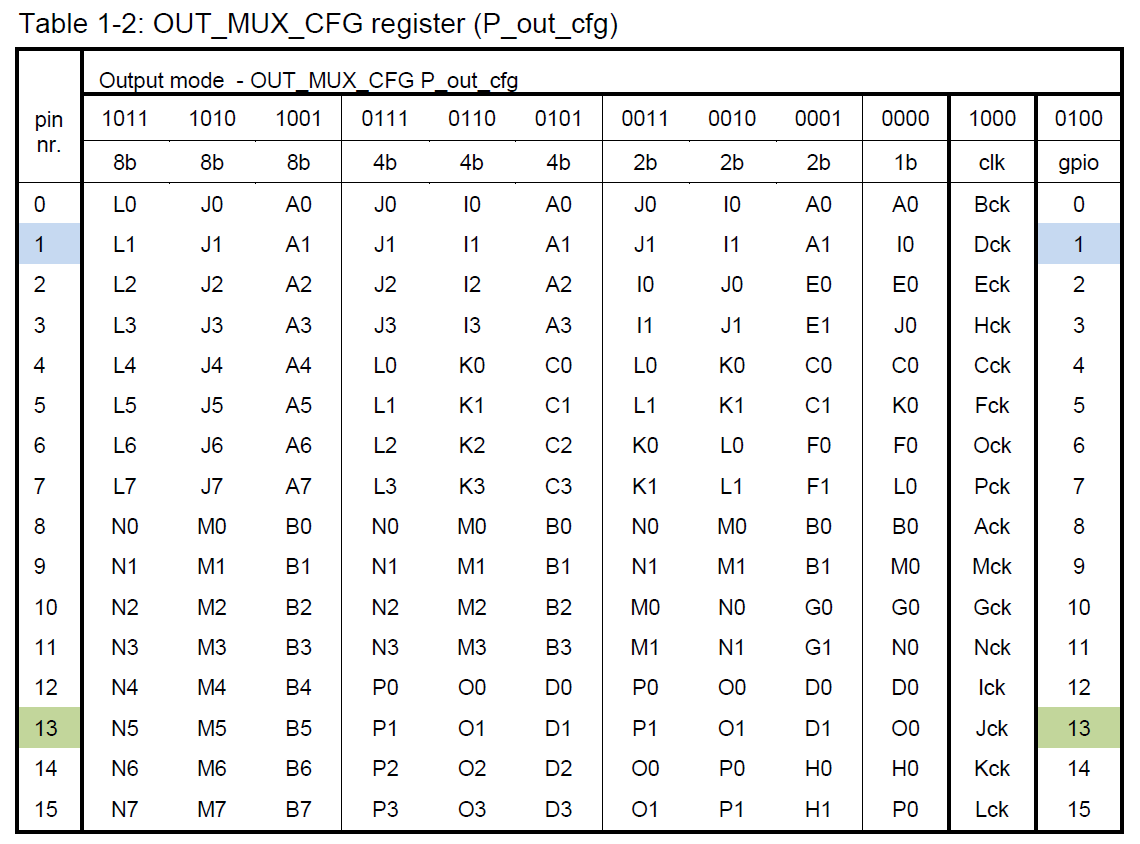
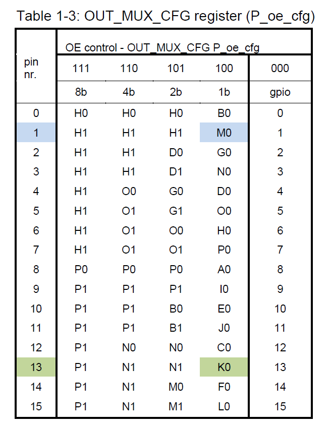
The output mode and output enable are set by the register called OUT_MUX_CFG as shown in Table 1-4.
In this demo, the value of bit 1 in GPIO_OUTREG is set to be always 0 in I2C implementation.
So, during I2C data sending,
the output of SGPIO 1 is 1 when slice M generates 0.
The output of SGPIO 1 is 0 when slice M generates 1.
The method above is applied to SGPIO 13 as well.
In this way, SGPIO could work well with I2C slave/master hardware construction (refer to Figure 1-10).
I2C Slice Configuration
SGPIO 1, the SDA signal pin, needs to get the state of buttons by receiving data.
So, one slice should be chosen to get the external data input from SGPIO 1.
According to Table 1-5 (see blue blocks), it is Slice I that is mapped as input to SGPIO 1.
As to get external data pin input for Slice I, set 0 in concat_enable bit in SGPIO_MUX_CFG register (refer to Table 1-6).
Table 1-5: Slices selection for Input or clock source (SGPIO_MUX_CFG register)
Another important part to configure slices is the shift rate setting.
In order to keep all the slices work at the same shift rate, 4 registers (SGPIO_MUX_CFG, PRESET, COUNT, and POS) should be set:
- SGPIO_MUX_CFG:
slice I, M, K are set to use slice D as their clock source. (refer to orange blocks in Table 1-5) - PRESET: controls the shift clock frequency by formula below.
So set same value to slice I, M, D, K.
frequencyshift_clock = frequencySGPIO_CLOCK / (PRESET+1) - COUNT: controls the phase of shift clock. Set 0 to slice I, M, D, K in this situation.
- POS: contains POS_COUNTER and POS_PRESET.
In this demo, slice exchange content between REG and REG_SS every 32 bits.
So values in POS_COUNTER and POS_PRESET should be 32 - 1 = 0x1F.

I2C Programming
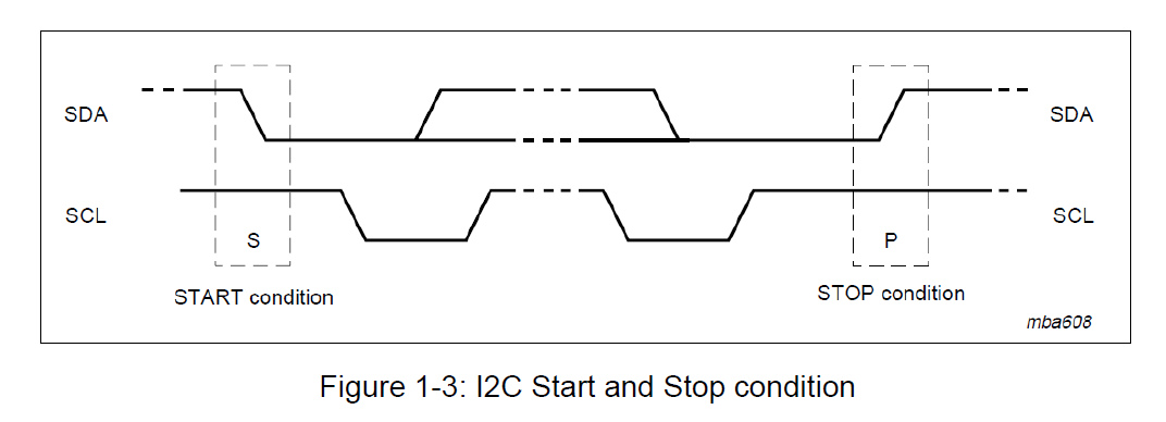
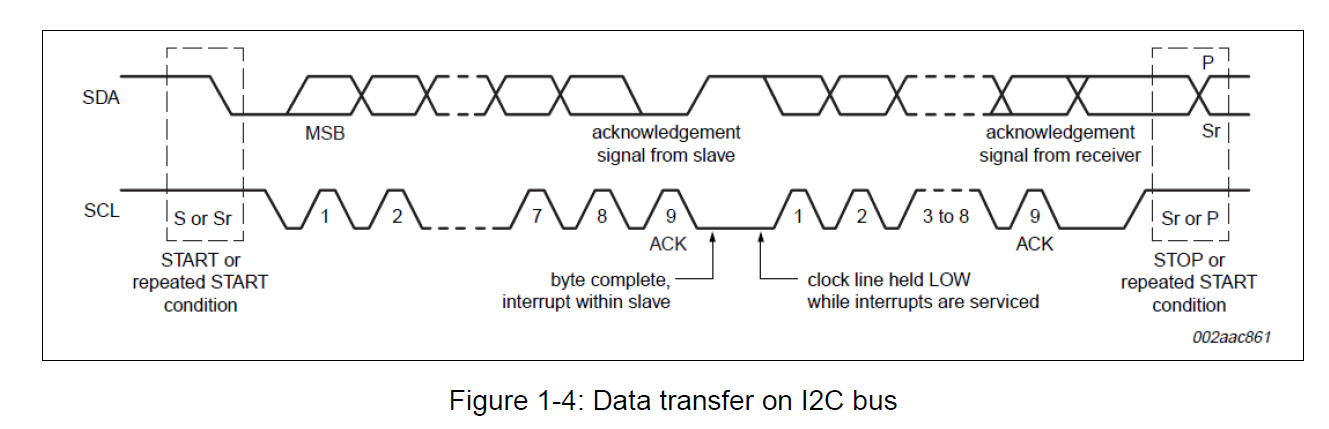
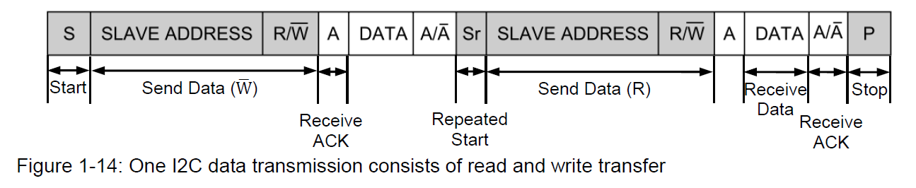
A basic I2C write transfer consists of
a START condition, followed by 7 address bits,
a one to indicate that it’s a write, an ACK (send by the slave),
8 data bits and another ACK, finalized with a stop condition.
The transfer is not an upfront fixed sequence as it depends on two conditions.
One is that what the acknowledge responses from the slave is.
The other is how many bytes of data would be sent.
Due to this, it makes sense to split the pattern to make it possible to respond to the feedback from the slave.
It’s also easier to perform a read transfer by separating protocol format into parts.
The I2C protocol is such that it is possible to stall the transfer.
The SGPIO is using 32 bit registers.
So the implementation is simpler if the transfer is split into parts which fit in 32 bit words.
This approach results in 8 parts:
Start, Send Data, Receive ACK/NACK, Repeated Start, Receive Data, Send ACK, Send NACK, and Stop.
These eight parts could group into several different combinations.
Three typical combinations are as follows:
- 1. Write to slave:
Start, Send slave address (/W), Receive ACK, Send data, Send NACK, Stop - 2. Read from slave:
Start, Send slave address (R), Receive ACK, Receive data, Send NACK, Stop - 3. Write and read:
Start, Send slave address (/W), Receive ACK, Send data, Receive ACK,
Repeated Start, Send slave address (R), Receive ACK, Receive Data, Send NACK, Stop (see Figure 1-14).
The data transmission is programmed to be a function named I2C_TransferData.
Eight parts mentioned above are programmed as eight functions and could be called in function I2C_TransferData.
The aim of function I2C_TransferData is to combine all possibilities of transfer formats.
It can choose whether to read or write and when.
Moreover, the function can react to acknowledge signal sent by slave.
It’s also possible to judge the validity of data sent by slave and response to it.
The input of I2C_TransferData function is a structure which contains
slave address, data length (means how many bytes of data) to send or receive, value of data to send or receive, counter of transferred bytes.
The data received is transferred back by this structure as well.
The output of the function is state of transmission, error or success.
Below are the flow charts of the I2C_TransferData function.
The gray block (Receive) in the left chart points to the gray block (Start Receive) in the right chart.
The Stop Receive block in the chart on the right points back to end of chart on the left.
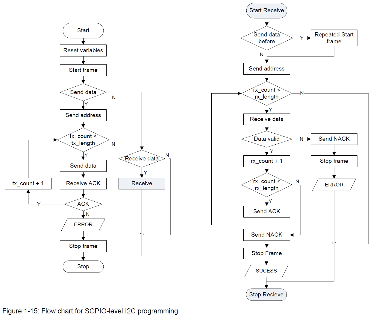
The function has Start and Stop at the beginning and the end respectively, and in between is data streaming.
Followed by START condition, it’s the decision whether to send data or not.
If sending data is needed, it starts to send 7-bit slave address with 8th bit low (/W), and then send data.
Followed by every byte sent, there are acknowledge receiving and judging if all the data has been sent.
The transmission could stop and send error information if the received acknowledge bit is high (NACK).
If there’s no need to send any data, or all data bytes have been sent successfully, the code will go to next decision.
This decision is to decide whether to read or not.
If reading is required, the routine will go to the flow chart on the right,
and decide whether to send a Repeated START condition or not.
If the transmission has sent data before receiving, a Repeated START condition is needed. < Write and Read >
Otherwise, the data transfer directly goes to address sending part.
Next, it sends 7-bit slave address with 8th bit high (R), receives 8-bit data, and checks the data validity to decide to send ACK or NACK.
If data is not stable on SDA when SCL is high, the transmission would generate a NACK and STOP condition.
Error information will be returned as well.
After receiving every data byte and sending ACK, the code will check if it reaches the amount of byte desired to receive.
If the decision is no data to receive, or all data bytes have been received successfully, the transmission will end with a STOP condition.
An important point to notice is that the last acknowledge bit sent before STOP condition should be NACK.
Otherwise, the slave would not recognize it’s the STOP condition to come.
Due to the 32-bit shift register and 8-bit data format,
extending 8-bit data into 32 bits is used in Send Data part,
and shortening 32 bits into 8 bits is used in Receive Data.
In this project, there are two boards used.
At the beginning of the project, an old board was used, which contains the touch buttons, LED, and PCA9502 as the slave.
The new board that was delivered later has push buttons, LED, joystick and PCA9673PW.
PCA9502 is an 8-bit I/O expander with I2C-bus or SPI interface.
It requires writing a register address of PCA9502 before read or write data.
Therefore, some sequences with using the old board contain read and write transfer, and appear like what is in Figure 1-14.
Since the working way of the new chip in the new board is different, data transmissions is either a read transfer or a write transfer.
So, not all the eight parts are actually working in the latest demo.
The structure of six functions above is very similar.
The basic idea is to change the values in REGi (i : represents the slice number)
and REG_SSi of output enable slices to generate different patterns.
Changing the values at the right time is the main difficulty.
For example, if a new value is written into REGi without any condition, the former pattern is changed to new one before it totally shifts out.
In a result, the pattern generated in this way is mixed with the previous value and the new value.
So a feature of SGPIO is used in this case.
The shift register REGi can shift out 32 bits and stop after exchanging with REG_SSi.
In other words, POSi could countdown once in one cycle of 32 bits if it is desired.
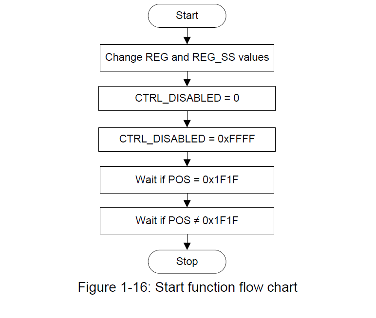
Detail steps are included in the example with Slice A (0) below.
CTRL_ENABLED = 0 (clear enable of all slices)
CTRL_DISABLED = 0 (clear disable of all slices)
REG[0] = 0xFFFF0000 (give a initial value of output)
CTRL_ENABLED = 1 (enable slice A which is now shifting sixteen 0s and sixteen 1s)
CTRL_DISABLED = 1 (slice A will shift one more old pattern and stop)
Wait (until POS_COUNTER reloads its value)
REG[0] = 0xFFFFFFFF (change a new value to output)
CTRL_DISABLED = 0; (slice A generates all high continually as new pattern)
In terms of right time to change value, the delay part above is made of two while loops in the demo, here is one example for slice K:
while (LPC_SGPIO->POS[10]==0x1F1F);
while (LPC_SGPIO->POS[10]!=0x1F1F);
The second while-loop is to wait until POS reloads its value.
The reason to have the first while-loop is that, in the program, the delay sections (while loop) are often used.
When POS equals 0x1F1F and it costs some time counting down to 0x1F1E, 0X1F1D and so on.
The code would run very fast and skip some while loops if there’s only the second while.
So the first while is to avoid skipping steps in transmission.
Another important thing is that value in while-loop condition should be 0x1F1F rather than 0x0.
It’s because the shifting disabled function is designed to pause the sequence at the moment POS has reloaded the new value.
The flow chart of Start function is in Figure 1-16.
For Send Data, Receive ACK/NACK, Repeated Start, Receive Data, Send ACK, Send NACK, and Stop, only one thing should be changed.
That is the desired value to be written in REG and REG_SS of slice K and slice M.
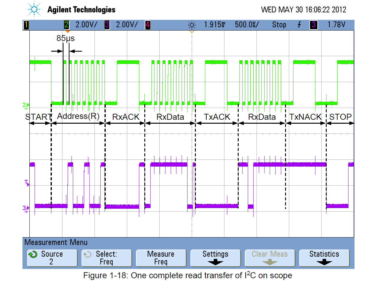
As shown in the figure, it’s a complete read transfer.
The master first generates START condition, sends slave address with 8th bit high,
and then keep SDA high on 9th clock to wait for the slave to send the acknowledge bit.
At this time the slave keeps driving SDA line low during 9th clock, it means the slave has received the address.
The master receives data in the next 8 clocks and then sends an ACK signal.
During next 8 clocks, the master receives another byte of data.
Then it's the master’s responsibility to send NACK to stop.
The master keeps SDA high to inform the slave to stop.
The whole transmission is terminated by a STOP condition.
Conclusion
I2C protocol could be implemented into SGPIO interface by software programming.
The demo proves it’s possible for SGPIO to work in rule of communication protocols.
Error detecting is also realizable.
There are still some problems left to be improved with I2C protocol:
- 1. The output of function I2C_TransferData is ERROR or SUCCESS.
It can be detected if there is any error during executing I2C_TransferData.
However, two conditions could lead to error state.
One is receiving NACK from slave when it sends address or data.
The other is the data received from slave couldn’t meet data validity.
When the routine get an error state of I2C_TransferData, it couldn’t define which part of the transfer generates error.
So it’s better to have overall information about where and what the error is. - 2. The wait part in Figure 1-16 is made of a while loop.
To wait until the exact moment, It’s better to have a smarter and safer solution instead of while loop. - 3. Now the code is working on ARM M4 core. The desired core to deal with peripherals is ARM M0.
- 4. Between M4/M0 core and SGPIO, there is a bridge.
The data stream should get over the bridge to reach SGPIO.
So it might cause latency when the sequence is complex and long.
A test of long data transmission is recommended to see the performance. - 5. I2C protocol contains Standard-mode, Fast-mode, Fast-mode Plus, and the High-speed mode.
The protocol achieved now is under Standard-mode. More work is left to realize other modes.

 浙公网安备 33010602011771号