JTAG Simplified
JTAG Simplified
So the other day, I explored the JTAG bus interface which is frequently found in CPLDs/FPGAs and is most of the times the sole method of programming and debugging them. It is a powerful interface and very easy to use. I intend to write about the interface and the protocol used for documentation purposes and knowledge sharing.
JTAG (Joint Test Action Group) started primarily as a debugging interface for CPLDs or more commonly boundary scan testing, which is explained later. The simplest implementation of the JTAG interface requires 4 signal wires, primarily
- TDO (Test Data Out) – This is output signal from the target in response to the test query.
- TDI (Test Data In) – This is the input signal for the target carrying the test query.
- TCK (Test Clock) – This is the synchronization clock signal
- TMS (Test-Mode Select) – This controls the TAP state, explained later.

Signals Explained
- TCK – is the JTAG clock signal. The other JTAG signals (TDI, TDO, TMS) are synchronous to TCK. So TCK has to toggle for anything to happen (usually things happen on TCK’s rising edge).
- TMS – Inside each JTAG IC, there is a JTAG TAP controller. The TAP controller is mainly a state machine with 16 states. TMS is the signal that controls the TAP controller. The TAP state diagram can be easily found in data-sheets of several JTAG ICs.The little numbers (“0” or “1”) close to each arrow are the value of TMS to change state. So for example, if a TAP controller is at state “Select DR-Scan” and TMS is “0” and TCK toggles, the state changes to “Capture-DR”.
- TDI and TDO – These signals carry the query and its response respectively. Referring to the TAP state diagram, Shift-DR and Shift-IR are the states where the query is generally pushed and Shift-DR is the state where the response is collected.
The TDI and TDO are daisy-chained. That is, with the Shift-DR size equal to 1-bit, data sent through the TDI starts coming back through the TDO after one clock pulse. Hence, when a response is to be collected from Shift-DR, clock pulses are sent to receive the response on the TDO. For example, if the Shift-DR size is 32 bits, 32 pulses are sent to completely receive the response of the JTAG query.
Registers
Each JTAG IC has one instruction register (IR) and multiple data registers (DR). Each instruction to the IR selects a different data register whose value is shifted out as explained above. For example, a 8-bit IR can select up to 256 DR, if available.
The length of each DR and IR registers can be found from the .bsdl file of the specific JTAG IC.
Instructions
The IR registers take in specific intructions which are listed in the .bsdl file of the JTAG IC. The most common of them grabbed from a .bsdl file are
attribute INSTRUCTION_LENGTH of EP1C3T100 : entity is 10;

attribute INSTRUCTION_OPCODE of EP1C3T100 : entity is
  "BYPASS            (1111111111), "&
  "EXTEST            (0000000000), "&
  "SAMPLE            (0000000101), "&
  "IDCODE            (0000000110), "&
  "USERCODE          (0000000111), "&
  "CLAMP             (0000001010), "&
  "HIGHZ             (0000001011), "&
  "CONFIG_IO            (0000001101)";

attribute INSTRUCTION_CAPTURE of EP1C3T100 : entity is "0101010101";

attribute IDCODE_REGISTER of EP1C3T100 : entity is
  "0000"&               --4-bit Version
  "0010000010000001"&   --16-bit Part Number (hex 2081)
  "00001101110"&        --11-bit Manufacturer's Identity
  "1";                  --Mandatory LSB

attribute BOUNDARY_LENGTH of EP1C3T100 : entity is 339;
Querying the JTAG Chain
Whenever the JTAG IC powers up it may end in any TAP state. Hence, it is mandatory to get it to a known state. One such method which is guaranteed to toggle the TAP state to Test-Logic-Reset is to hold TMS high for five clock cycles.
- Set TMS high.
- Send minimum of five clock cycles.
- Set TMS low.
1. Count number of ICs on the JTAG chain
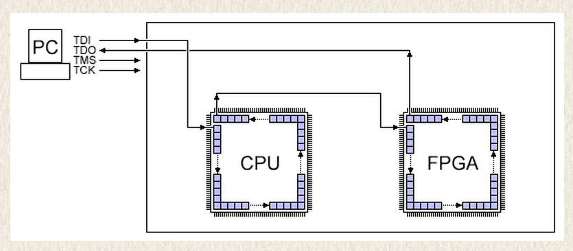
One important IR value is the “all-ones” value. For the CPU that would be 11111 and for the FPGA, that’s 1111111111. This value corresponds to the mandatory IR instruction called BYPASS. In bypass mode, the TAP controller DR register is always a single flip-flop which does nothing besides delaying the TDI input by one clock cycle before outputting to TDO.
One interesting way to use this BYPASS mode is to count the number of ICs that are present in the JTAG chain.
If each JTAG IC delays the TDI-TDO chain by one clock, we can send some data and check by how long it is delayed. That gives us the number of ICs in the chain.
2. Identify ICs on the JTAG Chain
The IDCODE instruction is used to identify ICs on the JTAG chain. The IDCODE instruction is automatically executed once the TAP state is forced to Test-Logic-Reset i.e the IDCODE data register appears on the TDO line. It is usually 32-bits long.
- Go to Test-Logic-Reset.
- Go to Shift-DR.
- Shift out 32 bits of data onto the TDO line by passing 32 clock pulses. LSB comes out first.
Similarly, other instruction can be passed to the IR and response read from the Shift-DR TAP state.
Boundary Scan Testing
This was the primary purpose of the JTAG interface when it was launched. In the boundary scan mode, the DR chain goes through each IO block and can read or hijack each pin.
Boundary-scan can be used even while a device is otherwise running. So for example, using JTAG on an FPGA, you can tell the status of each pin while the FPGA is running. The SAMPLE instruction is used in running a boundary scan. The .bsdl file lists the size of the boundary scan chain and the various pad configurations. In the .bsdl above, the length is 339 bits listed in the last line. Each pin use an IO pad on the IC die. Some IO pads use one, two or three bits from the chain (depending if the pin is input only, output with tri-state, or both). Also some registers correspond to IO pads that may not be bounded (they exists on the IC die but are not accessible externally). Which explains why a 100 pins device can have a 339 bits boundary-scan chain.
attribute BOUNDARY_REGISTER of EP1C3T100 : entity is
  --BSC group 0 for I/O pin 100
  "0   (BC_1, IO100, input, X)," &
  "1   (BC_1, *, control, 1)," &
  "2   (BC_1, IO100, output3, X, 1, 1, Z)," &

  --BSC group 1 for I/O pin 99
  "3   (BC_1, IO99, input, X)," &
  "4   (BC_1, *, control, 1)," &
  "5   (BC_1, IO99, output3, X, 4, 1, Z)," &

  ...
  ...
  ...

  --BSC group 112 for I/O pin 1
  "336 (BC_1, IO1, input, X)," &
  "337 (BC_1, *, control, 1)," &
  "338 (BC_1, IO1, output3, X, 337, 1, Z)" ;
This lists all the 339 bits of the chain, and what they do.
For example, bit 3 is the one that tells us what is the value on pin 99.
Querying the boundary scan chain is straightforward.
- Go to Shift-IR state.
- Shift in SAMPLE instruction with TMS low.
- Go to Exit1-IR.
- Go to Shift-DR.
- In our case, the data register is 339 bits long, Read the contents of the Shift-DR over TDO by sending 339 clock pulses with TMS low.
Using the JTAG interface, is pretty simple. It is basically a serial interface with a ‘cool’ name. You shift out a query and shift in the response. Knowledge of this interface is essential as its use is increasing day by day. Almost every microprocessor now uses it as a primary hardware debugging interface.

 浙公网安备 33010602011771号