电源切换电路 负载开关电路


This circuit is much simpler than it sounded like it was going to need to be,
due to the revelation that the USB power feed could easily accomodate a Schottky "blocking dioe"
and still meet the Vout requirement.
If this diode had had too high a voltage drop to be acceptable then a circuit withtime delays
and current flow direction detection would hav ebeen needed.
It can be surprising how much difference a little more information can make to the solution of a problem.
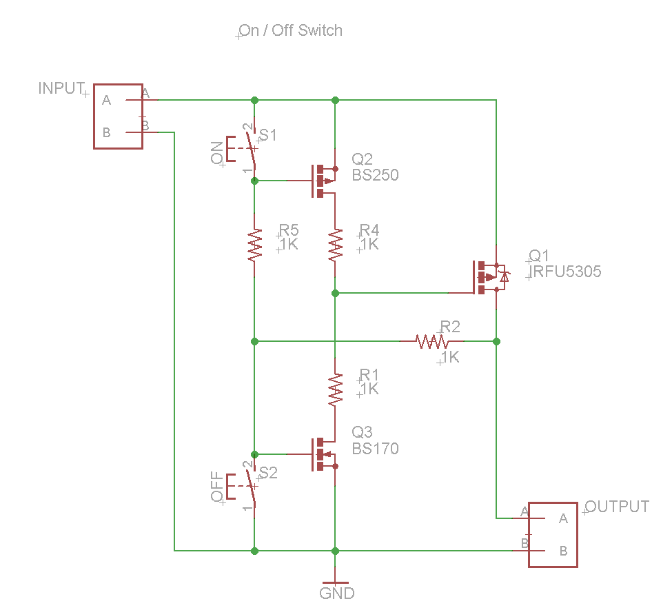
Battery feed at top. USB power feed at bottom.
USB power is fed to load via Schottky diode D1. Power may be fed via Ja and the LDO regulator or via JB as desired.
If feed via JB is used the LDO must survive with external voltage on its output when it has no input.
If necessary (depends on LDO) adding another Schottky diode across Ja "pointing upwards"
would apply the same voltage across either side of the LDO and minimise quiescent current (in most cases)
when USB power is in use.
If absolutely necessary another FET could be used to block USB feed from LDO but should not be needed.
LDO could be put above Q3 BUT then battery supplies LDO quiescent current at all times = poor.
When USB voltage is absent Q3 = P Channel MOSFET is turned on by R4, feeding battery voltage to LDO and thence to Vout.
When USB voltage is present Q1 is trurned on by R2/R3 and this turns on Q2 (usually held off by R1)
which clamps Q3 gate high turning it off, thus disabling battery feed. USB power feeds via D1 either via Ja and LDo or Jb as above.
Battery current when USB connected:
Changed R1, R4, R5 to nominal 1 megohm each to reduce battery load when USB in use.
A small MOSFET for Q2 and/or some more thinking will reduce required standby current.
USB on, Q1 on, About 5 uA via R5 to turn Q2 on.
About 5 uA via R4 to turn Q3 off.
R4 can probably be 10M if slow response OK.
( At R4 = 10 megohm if gate capcitance on Q3 is say 10 nF then time constant for turn on = RC = 1E7 x 10E-9 =~ 0.1 second.
Depending on =FET gate threshold it MAY take a few 10ths of a secind for battery to turn on when USB is unplugged.
This could dropout powered cct unless a large enough output cap was provided.
At R4 = 1m the time constant is about 10 milliseconds and a "usual" sort of cap on output rail would suffice.
Can be "tuned". Q1 on removes voltage from R1. 10 uA quiescent when USB is on =~ 90 mAh/year.
This is about 3% of battery pack capacity. Small but annoying.
Q1, Q2 = almost any jellybean bipolar.
Q3 = P Channel MOSFET. Vthreshold << Vbattery.
D1 = Schottky eg 1N5817.
LDO to suit.
Roll your own LDO with MOSFET and eg TLV431 can have about 100 uA quiescent
when running and essentially zero dropout voltage.
Can be much lower with lower Iq ref diode.
BUT When you can get eg Microchip's VERY nice TC2104 LDO for under 50 cents in 1's, making your own makes less sense.

why are the BJTs needed?
Why not just have a MOSFET and a diode, and that's it?
The MOSFET solution is a good one but it is slightly more design-demanding than may be apparent,
whereas the bipolar solution uses a few more components but is easier to ensure operation ioj all conditions.
Tpo use the MOSFET as shown the FET's Vgsth must be chosen to suit.
Battery max voltage (assuming his AA cells are Alkaline) is 1.65V (new cells) x 4 = 6.6V.
In a few cases even maybe 1.655V so say 6.8V for 4.
USB is say 5.3V max when on and 0V when off after any capacitors discharge.
But critical here is not USB Vmax but USB_on_min : USB_on_min = say 4.8V.
Under that condition FET must be off, so FET Vgs = (6.8-4.8) =~~~~ 2V worst case.
The FET MUST NOT turn on at Vgs = 2V.
Battery min is say 4V and USB low falls to 0V "after a while" so FET must turn on at Vgs = 4V.
That puts the FET Vgs_off_max and Vgs_on_min in a fairly narrow 2 to 4V range.
That's certainly doable by correct choice of FET - but datasheet must be chacked to ensure that worst case spread lies in the desired range.
The designer needs to be aware that design is needed!
In the bipolar case the USB Von_min is very easily accommodated by Q1
and if desired full turnoff can occur when V_USB is say 2V so changeover to battery is better defined.
So overall, the bipolar addition adds 2 x Q and 4 x R (small but non trivial) for the sake of better flexibility and designability.
BUT the MOSFET only solution is a good one as long as the complexity that goes along with the simplicity is properly understood.
current is a lot (the typical load is perhaps 500 mA, but peak load on the device is 10 A. )
This is the best I could come up with.
De-bouncing the buttons is not needed.
When first connected, I think it enters "off" state
because the gate is weakly pulled to ground through the load (output) - and even if it isn`t,
the main power P-channel FET isn`t going to have any gate charge.
If you want to spend a few minutes helping out a poor n00b on circuit design,
please critique this design and suggest whatever you think needs improving in this circuit.
(Three FETs really ) If you think my diagram is hard to read (I got that last time :-)
then please at least critique exactly what you think is poor about the diagram,
so that I can better communicate in the future.


The Arduino Duemilanove can be powered via the USB connection or with an external power supply.
The power source is selected automatically.
External (non-USB) power can come either from an AC-to-DC adapter (wall-wart) or battery.
The adapter can be connected by plugging a 2.1mm center-positive plug into the board's power jack.
Leads from a battery can be inserted in the Gnd and Vin pin headers of the POWER connector.
The board can operate on an external supply of 6 to 20 volts.
If supplied with less than 7V, however, the 5V pin may supply less than five volts and the board may be unstable.
If using more than 12V, the voltage regulator may overheat and damage the board.
The recommended range is 7 to 12 volts.
The power pins are as follows:
-
VIN. The input voltage to the Arduino board when it's using an external power source
(as opposed to 5 volts from the USB connection or other regulated power source).
You can supply voltage through this pin, or, if supplying voltage via the power jack, access it through this pin. -
5V. The regulated power supply used to power the microcontroller and other components on the board.
This can come either from VIN via an on-board regulator, or be supplied by USB or another regulated 5V supply. -
3V3. A 3.3 volt supply generated by the on-board FTDI chip. Maximum current draw is 50 mA.
-
GND. Ground pins.


If your microcontroller can tolerate 5 volts on its output pins,
then you could hook up the output directly to the gate of the P-channel MOSFET in an open-drain configuration,
and not need the N-channel device.
R1 is there to insure the MOSFET is on when the N-channel MOSFET is off.
Because of the inverting nature of the N-channel MOSFET,
a 0 on the output of the microcontroller turns on the load,
and 1 turns it off. Adding a pull-up (R2) to 3.3v on the output of the microcontroller
keeps the load off when the circuit first comes up.
You will want to configure the microcontroller's output pin as open-drain.
Note there are no resistors in the gate circuits of the FETs,
this is because they are voltage-driven devices unlike BJT's whose bases are current-driven.
The DMP2035U has a typical Rds(on) of 23 mΩ and can handle 2.9A continuous,
and dissipate 0.8W. So the voltage drop will be about 45 mV, or about 4.95v across the load.
Load Switch with Level-Shift
The Si1869DH includes a p- and n-channel MOSFET in a single SC70-6 package.
The low on-resistance p-channel TrenchFET is tailored for use as a load switch.
The n-channel, with an external resistor, can be used as a levelshift to drive the p-channel load-switch.
The n-channel MOSFET has internal ESD protection and can be driven by logic signals as low as 1.5 V.
The Si1869DH operates on supply lines from 1.8 V to 20 V, and can drive loads up to 1.2 A.


TPS27081A 1.2-V to 8-V, 3-A PFET High-Side Load Switch With Level Shift and Adjustable Slew Rate Control

NTGD1100L


In the steady state on mode the "problem" is easily addressed.
-
A given MOSFET will have a well defined on resistance at a given gate drive voltage. This resistance will change with temperature, but usually by less than 2:1.
-
For a given MOSFET you can usually decrease on resistance by increasing gate drive voltage, up to the maximum allowed for the MOSFET.
-
For a given load current and gate drive voltage you can choose the MOSFET with the lowest on state resistance that you can afford.
-
You can get MOSFETS with Rdson in the 5 to 50 milliohm range at currents of up to say 10A at reasonable cost. You can get similar at up to say 50A at increasing cost.
Examples:
In the absence of good information I'll make some assumptions.
These can be improved by providing actual data.
Assume 12V to be switched at 10A.
Power = V x I = 120 Watts.
With an Rdson hot of 50 milliohms the power dissipation in the MOSFET will be
I^2 x R = 10^2 x 0.05 = 5 Watts = 5/120 or about 4% of the load power.
You would need a heatsink on almost any package.
At 5 milliohms Rdson hot dissipation would be 0.5 Watts. and 0.4% of load power.
A TO220 in still air would handle that OK.
A DPak / TO252 SMD with minimal PCB copper would handle that OK.
As an example of an SMD MOSFET that would work well.
2.6 milliohms Rdson best case.
Say about 5 milliohms in practice. 30V, 60A rated. $1 in volume.
Probably a few $ in 1's. You would not ever use the 60A - that's a package limit.
At 10A that's 500 mW dissipation, as above.
Thermal data is a little uncertain but it sounds like 54 C/Watt junction to ambient on a 1" x 1" FR4 PCB steady state.
So about 0.5W x 54 C/W = 27C rise.
Say 30C. In an enclosure you'll get a junction temperature of maybe 70-80 degrees.
Even in Death Valley in midsummer it should be OK.
[Warning: DO NOT shut the door on the toilet at Zabriski Point in mid summer !!!!]
[Even if you are a woman and the Hell's Angels or similar have just arrived]
[My wife will tell you about it]
[But your MOSFET would be OK.]
For $1.77/1 you get a rather nice TO263 / DPak device.
30v, 90A, 62 K/W with minimal copper and 40 k/W with a whisper.
This is an awesome MOSFET in this type of application.
Under 5 milliohms achievable at many 10's of amps.
If you could access the actual die you could possibly start a small car with this as the starter motor switch
(spec'd to 360A on graphs) BUT the bondwires are rated at 90A.
ie the MOSFET inside greatly exceeds the package capability.
At say 30A power = I^2 x R = 30^2 x 0.003 = 2.7W.
0.003 ohms seems fair after looking at the data sheet.


ADP199是一个高侧的负荷开关设计为0.9 V至3.6 V提供电源域隔离负荷开关操作,从而有助于保持孤立和独立供电的子系统,并实现降低功耗。
ADP199包含一个低导通电阻,N沟道MOSFET功率损耗降到最小,并支持连续负载电流超过500毫安。
低静态电流和超低停机电流的电池供电的便携式设备的ADP199理想 。
内置的水平移位为使逻辑ADP199与许多处理器和兼容的GPIO控制器。
MOSFET驱动器是电池反向保护-MOSFET Driver

Figure 1. An external p-channel MOSFET (Q1) easily protects this MOSFET driver (U1) against reversed batteries and reversed load current.
Abstract: MOSFET power-switch drivers must be protected from a reverse-battery connection. A small rectifier diode can protect against reversed batteries, but that approach is generally unacceptable for systems in which battery life is crucial. For a 6V battery, the diode's forward voltage drop (0.6V to 0.7V typical) produces a constant power loss of approximately 10%, which increases with dwindling battery voltage. An improvement over single-diode protection is shown.
MOSFET power-switch drivers must be protected from a reverse-battery connection. A small rectifier diode can protect against reversed batteries, but that approach is generally unacceptable for systems in which battery life is crucial. For a 6V battery, the diode's forward voltage drop (0.6V to 0.7V typical) produces a constant power loss of approximately 10%, which increases with dwindling battery voltage.
Figure 1 illustrates an improvement over single-diode protection.
A p-channel MOSFET (Q1) protects the driver (U1) from reverse-battery insertion.
Q1's low on-resistance of 10mΩor less produces a forward-voltage drop of only a few millivolts
(vs. hundreds of millivolts for a diode).
Thus, substituting a MOSFET for the diode provides an immediate improvement in efficiency.
Connecting a positive battery voltage to the drain of Q1 produces forward bias in its body diode,
which clamps the source voltage one diode drop below the drain voltage.
When the source voltage exceeds Q1's threshold voltage, Q1 turns on.
Once the FET is on, the battery is fully connected to the system and can deliver power to U1 and the load.
An incorrectly inserted battery reverse-biases the body diode.
The source remains at ground potential and the gate is connected to ground,
so Q1 remains off, disconnecting the reversed battery from the system.
VDS equals the full negative battery voltage when you insert the battery backwards,
and in some applications Q1 may have to withstand transient levels many times the battery voltage.
Q1 must be able towithstand VGS and VDS voltages at least equal to the maximum battery voltage.
Besides reverse-battery protection, the Figure 1 circuit also protects against reverse load current at startup.
Q3 ensures that no load current flows until U1 enables both n-channel MOSFETs (Q2 and Q3).
Reverse load current can cause Q1 to turn on inadvertently,
leaving the circuit unprotected against reversed-battery connections.

 浙公网安备 33010602011771号