
(原創) 如何產生VGA的Color Pattern Generator? (SOC) (Verilog) (DE2) (DE2-70)
 本文使用Verilog在VGA產生Color Pattern Generator。
Abstract
本文使用Verilog在VGA產生Color Pattern Generator。
Introduction
使用環境:Quartus II 8.0 + DE2(Cyclone II EP2C35F627C6) or DE2-70 (Cyclone II EP2C70F896C6N)
DE2_70.v / Verilog
1 /*
2 (C) OOMusou 2008 http://oomusou.cnblogs.com
3
4 Filename : DE2_70.v
5 Compiler : Quartus II 8.0
6 Description : Demo how to write color pattern generator
7 Release : 11/16/2008 1.0
8 */
9
10 module DE2_70 (
11 //////////////////////// Clock Input ////////////////////////
12 input iCLK_28, // 28.63636 MHz
13 input iCLK_50, // 50 MHz
14 input iCLK_50_2, // 50 MHz
15 input iCLK_50_3, // 50 MHz
16 input iCLK_50_4, // 50 MHz
17 input iEXT_CLOCK, // External Clock
18 //////////////////////// Push Button ////////////////////////
19 input [3:0] iKEY, // Pushbutton[3:0]
20 //////////////////////// DPDT Switch ////////////////////////
21 input [17:0] iSW, // Toggle Switch[17:0]
22 //////////////////////// 7-SEG Dispaly ////////////////////////
23 output [6:0] oHEX0_D, // Seven Segment Digit 0
24 output oHEX0_DP, // Seven Segment Digit 0 decimal point
25 output [6:0] oHEX1_D, // Seven Segment Digit 1
26 output oHEX1_DP, // Seven Segment Digit 1 decimal point
27 output [6:0] oHEX2_D, // Seven Segment Digit 2
28 output oHEX2_DP, // Seven Segment Digit 2 decimal point
29 output [6:0] oHEX3_D, // Seven Segment Digit 3
30 output oHEX3_DP, // Seven Segment Digit 3 decimal point
31 output [6:0] oHEX4_D, // Seven Segment Digit 4
32 output oHEX4_DP, // Seven Segment Digit 4 decimal point
33 output [6:0] oHEX5_D, // Seven Segment Digit 5
34 output oHEX5_DP, // Seven Segment Digit 5 decimal point
35 output [6:0] oHEX6_D, // Seven Segment Digit 6
36 output oHEX6_DP, // Seven Segment Digit 6 decimal point
37 output [6:0] oHEX7_D, // Seven Segment Digit 7
38 output oHEX7_DP, // Seven Segment Digit 7 decimal point
39 //////////////////////////// LED ////////////////////////////
40 output [8:0] oLEDG, // LED Green[8:0]
41 output [17:0] oLEDR, // LED Red[17:0]
42 //////////////////////////// UART ////////////////////////////
43 output oUART_TXD, // UART Transmitter
44 input iUART_RXD, // UART Receiver
45 output oUART_CTS, // UART Clear To Send
46 input iUART_RTS, // UART Requst To Send
47 //////////////////////////// IRDA ////////////////////////////
48 output oIRDA_TXD, // IRDA Transmitter
49 input iIRDA_RXD, // IRDA Receiver
50 /////////////////////// SDRAM Interface ////////////////////////
51 inout [31:0] DRAM_DQ, // SDRAM Data bus 32 Bits
52 output [12:0] oDRAM0_A, // SDRAM0 Address bus 13 Bits
53 output [12:0] oDRAM1_A, // SDRAM1 Address bus 13 Bits
54 output oDRAM0_LDQM0, // SDRAM0 Low-byte Data Mask
55 output oDRAM1_LDQM0, // SDRAM1 Low-byte Data Mask
56 output oDRAM0_UDQM1, // SDRAM0 High-byte Data Mask
57 output oDRAM1_UDQM1, // SDRAM1 High-byte Data Mask
58 output oDRAM0_WE_N, // SDRAM0 Write Enable
59 output oDRAM1_WE_N, // SDRAM1 Write Enable
60 output oDRAM0_CAS_N, // SDRAM0 Column Address Strobe
61 output oDRAM1_CAS_N, // SDRAM1 Column Address Strobe
62 output oDRAM0_RAS_N, // SDRAM0 Row Address Strobe
63 output oDRAM1_RAS_N, // SDRAM1 Row Address Strobe
64 output oDRAM0_CS_N, // SDRAM0 Chip Select
65 output oDRAM1_CS_N, // SDRAM1 Chip Select
66 output [1:0] oDRAM0_BA, // SDRAM0 Bank Address
67 output [1:0] oDRAM1_BA, // SDRAM1 Bank Address
68 output oDRAM0_CLK, // SDRAM0 Clock
69 output oDRAM1_CLK, // SDRAM1 Clock
70 output oDRAM0_CKE, // SDRAM0 Clock Enable
71 output oDRAM1_CKE, // SDRAM1 Clock Enable
72 //////////////////////// Flash Interface ////////////////////////
73 inout [14:0] FLASH_DQ, // FLASH Data bus 15 Bits (0 to 14)
74 inout FLASH_DQ15_AM1, // FLASH Data bus Bit 15 or Address A-1
75 output [21:0] oFLASH_A, // FLASH Address bus 26 Bits
76 output oFLASH_WE_N, // FLASH Write Enable
77 output oFLASH_RST_N, // FLASH Reset
78 output oFLASH_WP_N, // FLASH Write Protect /Programming Acceleration
79 input iFLASH_RY_N, // FLASH Ready/Busy output
80 output oFLASH_BYTE_N, // FLASH Byte/Word Mode Configuration
81 output oFLASH_OE_N, // FLASH Output Enable
82 output oFLASH_CE_N, // FLASH Chip Enable
83 //////////////////////// SRAM Interface ////////////////////////
84 inout [31:0] SRAM_DQ, // SRAM Data Bus 32 Bits
85 inout [3:0] SRAM_DPA, // SRAM Parity Data Bus
86 output [18:0] oSRAM_A, // SRAM Address bus 21 Bits
87 output oSRAM_ADSC_N, // SRAM Controller Address Status
88 output oSRAM_ADSP_N, // SRAM Processor Address Status
89 output oSRAM_ADV_N, // SRAM Burst Address Advance
90 output [3:0] oSRAM_BE_N, // SRAM Byte Write Enable
91 output oSRAM_CE1_N, // SRAM Chip Enable
92 output oSRAM_CE2, // SRAM Chip Enable
93 output oSRAM_CE3_N, // SRAM Chip Enable
94 output oSRAM_CLK, // SRAM Clock
95 output oSRAM_GW_N, // SRAM Global Write Enable
96 output oSRAM_OE_N, // SRAM Output Enable
97 output oSRAM_WE_N, // SRAM Write Enable
98 //////////////////// ISP1362 Interface ////////////////////////
99 inout [15:0] OTG_D, // ISP1362 Data bus 16 Bits
100 output [1:0] oOTG_A, // ISP1362 Address 2 Bits
101 output oOTG_CS_N, // ISP1362 Chip Select
102 output oOTG_OE_N, // ISP1362 Read
103 output oOTG_WE_N, // ISP1362 Write
104 output oOTG_RESET_N, // ISP1362 Reset
105 inout OTG_FSPEED, // USB Full Speed, 0 = Enable, Z = Disable
106 inout OTG_LSPEED, // USB Low Speed, 0 = Enable, Z = Disable
107 input iOTG_INT0, // ISP1362 Interrupt 0
108 input iOTG_INT1, // ISP1362 Interrupt 1
109 input iOTG_DREQ0, // ISP1362 DMA Request 0
110 input iOTG_DREQ1, // ISP1362 DMA Request 1
111 output oOTG_DACK0_N, // ISP1362 DMA Acknowledge 0
112 output oOTG_DACK1_N, // ISP1362 DMA Acknowledge 1
113 //////////////////// LCD Module 16X2 ////////////////////////////
114 inout [7:0] LCD_D, // LCD Data bus 8 bits
115 output oLCD_ON, // LCD Power ON/OFF
116 output oLCD_BLON, // LCD Back Light ON/OFF
117 output oLCD_RW, // LCD Read/Write Select, 0 = Write, 1 = Read
118 output oLCD_EN, // LCD Enable
119 output oLCD_RS, // LCD Command/Data Select, 0 = Command, 1 = Data
120 //////////////////// SD Card Interface ////////////////////////
121 inout SD_DAT, // SD Card Data
122 inout SD_DAT3, // SD Card Data 3
123 inout SD_CMD, // SD Card Command Signal
124 output oSD_CLK, // SD Card Clock
125 //////////////////////// I2C ////////////////////////////////
126 inout I2C_SDAT, // I2C Data
127 output oI2C_SCLK, // I2C Clock
128 //////////////////////// PS2 ////////////////////////////////
129 inout PS2_KBDAT, // PS2 Keyboard Data
130 inout PS2_KBCLK, // PS2 Keyboard Clock
131 inout PS2_MSDAT, // PS2 Mouse Data
132 inout PS2_MSCLK, // PS2 Mouse Clock
133 //////////////////////// VGA ////////////////////////////
134 output oVGA_CLOCK, // VGA Clock
135 output oVGA_HS, // VGA H_SYNC
136 output oVGA_VS, // VGA V_SYNC
137 output oVGA_BLANK_N, // VGA BLANK
138 output oVGA_SYNC_N, // VGA SYNC
139 output [9:0] oVGA_R, // VGA Red[9:0]
140 output [9:0] oVGA_G, // VGA Green[9:0]
141 output [9:0] oVGA_B, // VGA Blue[9:0]
142 //////////////// Ethernet Interface ////////////////////////////
143 inout [15:0] ENET_D, // DM9000A DATA bus 16Bits
144 output oENET_CMD, // DM9000A Command/Data Select, 0 = Command, 1 = Data
145 output oENET_CS_N, // DM9000A Chip Select
146 output oENET_IOW_N, // DM9000A Write
147 output oENET_IOR_N, // DM9000A Read
148 output oENET_RESET_N, // DM9000A Reset
149 input iENET_INT, // DM9000A Interrupt
150 output oENET_CLK, // DM9000A Clock 25 MHz
151 //////////////////// Audio CODEC ////////////////////////////
152 inout AUD_ADCLRCK, // Audio CODEC ADC LR Clock
153 input iAUD_ADCDAT, // Audio CODEC ADC Data
154 inout AUD_DACLRCK, // Audio CODEC DAC LR Clock
155 output oAUD_DACDAT, // Audio CODEC DAC Data
156 inout AUD_BCLK, // Audio CODEC Bit-Stream Clock
157 output oAUD_XCK, // Audio CODEC Chip Clock
158 //////////////////// TV Devoder ////////////////////////////
159 input iTD1_CLK27, // TV Decoder1 Line_Lock Output Clock
160 input [7:0] iTD1_D, // TV Decoder1 Data bus 8 bits
161 input iTD1_HS, // TV Decoder1 H_SYNC
162 input iTD1_VS, // TV Decoder1 V_SYNC
163 output oTD1_RESET_N, // TV Decoder1 Reset
164 input iTD2_CLK27, // TV Decoder2 Line_Lock Output Clock
165 input [7:0] iTD2_D, // TV Decoder2 Data bus 8 bits
166 input iTD2_HS, // TV Decoder2 H_SYNC
167 input iTD2_VS, // TV Decoder2 V_SYNC
168 output oTD2_RESET_N, // TV Decoder2 Reset
169 //////////////////////// GPIO ////////////////////////////////
170 inout [31:0] GPIO_0, // GPIO Connection 0 I/O
171 input GPIO_CLKIN_N0, // GPIO Connection 0 Clock Input 0
172 input GPIO_CLKIN_P0, // GPIO Connection 0 Clock Input 1
173 inout GPIO_CLKOUT_N0, // GPIO Connection 0 Clock Output 0
174 inout GPIO_CLKOUT_P0, // GPIO Connection 0 Clock Output 1
175 inout [31:0] GPIO_1, // GPIO Connection 1 I/O
176 input GPIO_CLKIN_N1, // GPIO Connection 1 Clock Input 0
177 input GPIO_CLKIN_P1, // GPIO Connection 1 Clock Input 1
178 inout GPIO_CLKOUT_N1, // GPIO Connection 1 Clock Output 0
179 inout GPIO_CLKOUT_P1 // GPIO Connection 1 Clock Output 1
180 );
181
182 // Horizontal Parameter
183 parameter H_FRONT = 16;
184 parameter H_SYNC = 96;
185 parameter H_BACK = 48;
186 parameter H_ACT = 640;
187 parameter H_BLANK = H_FRONT + H_SYNC + H_BACK;
188 parameter H_TOTAL = H_FRONT + H_SYNC + H_BACK + H_ACT;
189
190 // Vertical Parameter
191 parameter V_FRONT = 11;
192 parameter V_SYNC = 2;
193 parameter V_BACK = 32;
194 parameter V_ACT = 480;
195 parameter V_BLANK = V_FRONT + V_SYNC + V_BACK;
196 parameter V_TOTAL = V_FRONT + V_SYNC + V_BACK + V_ACT;
197
198 wire CLK_25;
199 wire CLK_to_DAC;
200 wire RST_N;
201
202 PLL pll0 (
203 .inclk0(iCLK_50),
204 .c0(CLK_25)
205 );
206
207 // Select DAC clock
208 assign CLK_to_DAC = CLK_25;
209 assign oVGA_SYNC_N = 1'b0; // This pin is unused.
210 assign oVGA_BLANK_N = ~((H_Cont<H_BLANK)||(V_Cont<V_BLANK));
211 assign oVGA_CLOCK = ~CLK_to_DAC; // Invert internal clock to output clock
212 assign RST_N = iKEY[0]; // Set reset signal is KEY[0]
213
214 reg [10:0] H_Cont;
215 reg [10:0] V_Cont;
216 reg [9:0] vga_r;
217 reg [9:0] vga_g;
218 reg [9:0] vga_b;
219 reg vga_hs;
220 reg vga_vs;
221 reg [10:0] X;
222 reg [10:0] Y;
223
224 assign oVGA_R = vga_r;
225 assign oVGA_G = vga_g;
226 assign oVGA_B = vga_b;
227 assign oVGA_HS = vga_hs;
228 assign oVGA_VS = vga_vs;
229
230 // Horizontal Generator: Refer to the pixel clock
231 always@(posedge CLK_to_DAC, negedge RST_N) begin
232 if(!RST_N) begin
233 H_Cont <= 0;
234 vga_hs <= 1;
235 X <= 0;
236 end
237 else begin
238 if (H_Cont < H_TOTAL)
239 H_Cont <= H_Cont+1'b1;
240 else
241 H_Cont <= 0;
242
243 // Horizontal Sync
244 if(H_Cont == H_FRONT-1) // Front porch end
245 vga_hs <= 1'b0;
246
247 if(H_Cont == H_FRONT + H_SYNC -1) // Sync pulse end
248 vga_hs <= 1'b1;
249
250 // Current X
251 if(H_Cont >= H_BLANK)
252 X <= H_Cont-H_BLANK;
253 else
254 X <= 0;
255 end
256 end
257
258 // Vertical Generator: Refer to the horizontal sync
259 always@(posedge oVGA_HS, negedge RST_N) begin
260 if(!RST_N) begin
261 V_Cont <= 0;
262 vga_vs <= 1;
263 Y <= 0;
264 end
265 else begin
266 if (V_Cont<V_TOTAL)
267 V_Cont <= V_Cont + 1'b1;
268 else
269 V_Cont <= 0;
270
271 // Vertical Sync
272 if (V_Cont == V_FRONT-1) // Front porch end
273 vga_vs <= 1'b0;
274
275 if (V_Cont == V_FRONT + V_SYNC-1) // Sync pulse end
276 vga_vs <= 1'b1;
277
278 // Current Y
279 if (V_Cont >= V_BLANK)
280 Y <= V_Cont-V_BLANK;
281 else
282 Y <= 0;
283 end
284 end
285
286 // Pattern Generator
287 always@(posedge CLK_to_DAC, negedge RST_N) begin
288 if(!RST_N) begin
289 vga_r <= 0;
290 vga_g <= 0;
291 vga_b <= 0;
292 end
293 else begin
294 vga_r <= (Y < 120) ? 256 :
295 (Y >= 120 && Y < 240) ? 512 :
296 (Y >= 240 && Y < 360) ? 768 :
297 1023;
298
299 vga_g <= (X < 80) ? 128 :
300 (X >= 80 && X < 160) ? 256 :
301 (X >= 160 && X < 240) ? 384 :
302 (X >= 240 && X < 320) ? 512 :
303 (X >= 320 && X < 400) ? 640 :
304 (X >= 400 && X < 480) ? 768 :
305 (X >= 480 && X < 560) ? 896 :
306 1023;
307
308 vga_b <= (Y < 60) ? 1023:
309 (Y >= 60 && Y < 120) ? 896 :
310 (Y >= 120 && Y < 180) ? 768 :
311 (Y >= 180 && Y < 240) ? 640 :
312 (Y >= 240 && Y < 300) ? 512 :
313 (Y >= 300 && Y < 360) ? 384 :
314 (Y >= 360 && Y < 420) ? 256 :
315 128;
316 end
317 end
318
319 endmodule
執行結果
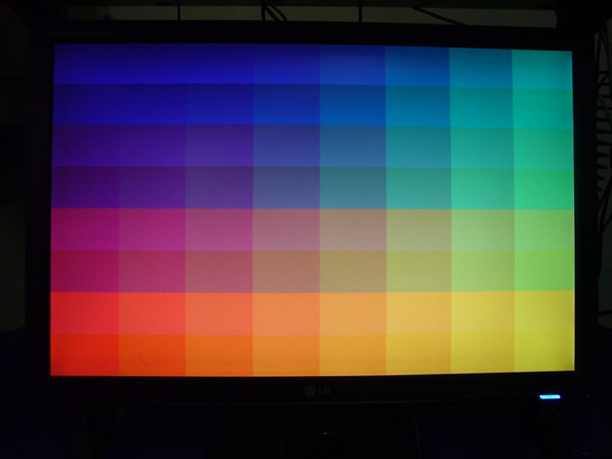
程式碼的解釋在都寫在註解裡了,我就不再多言。初學者可能會遇到幾個問題:
1.VGA Timing部分:
這在網上討論很多,讀者可自行google,我舉一篇讓各位參考:VGA显示原理与VGA时序实现
2.若欲更改解析度與頻率:
請參考(筆記) D-Sub VGA timing table (SOC) (DE2) (DE2-70),自行更改parameter。
3.若欲更改顏色與座標:
請參考(原創) 如何控制DE2 VGA輸出時某座標的顏色? (IC Design) (DE2) (Quartus II)
完整程式碼下載
DE2_VGA_pattern_gen.7z (for DE2)
DE2_70_VGA_pattern_gen.7z (for DE2-70)
See Also
(筆記) D-Sub VGA timing table (SOC) (DE2) (DE2-70)
(原創) 如何控制DE2 VGA輸出時某座標的顏色? (IC Design) (DE2) (Quartus II)
(原創) 如何控制TRDB-LTM輸出時某座標的顏色? (SOC) (DE2-70) (TRDB-LTM)


