

(原創) 如何在Nios II對Flash進行讀寫? (SOC) (Nios II) (DE2) (DE2-70)
 在DE2版子上,除了8MB的SDRAM最大外,排名第2的就是4MB的Flash,本文討論如何在Nios II對Flash進行讀寫。
Abstract
在DE2版子上,除了8MB的SDRAM最大外,排名第2的就是4MB的Flash,本文討論如何在Nios II對Flash進行讀寫。
Introduction
使用環境:Quartus II 8.0 + Nios II EDS 8.0 + DE2(Cyclone II EP2C35F627C6) or DE2-70 (Cyclone II EP2C70F896C6N)
我曾經在(原創) 如何在Nios II使用Zip File System? (IC Design) (Nios II) (DE2)與(原創) 如何讓Nios II一Power On就執行? (SOC) (Nios II) (SOPC Builder) (DE2) (DE2-70)討論對flash的使用,不過那只能算是『應用』,並未真的用HAL去存取過flash,剛好網友成電王超提到用HAL讀寫flash的問題,我就順手測試了一下。
以DE2_NIOS_Lite 1.2為範本
我使用(原創) DE2_NIOS_Lite 1.2 (SOC) (Nios II) (SOPC Builder) (DE2)為範本測試flash,這個SOPC已經將flash ip掛好,所以我們可以將重點放在HAL部分,不過考量有些人是自己建立SOPC系統,還是討論一下SOPC部分。
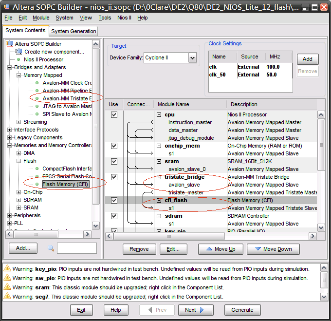
SOPC Builder部分
Step 1:
掛上Tristate Bridge與Flash Memory(CFI)
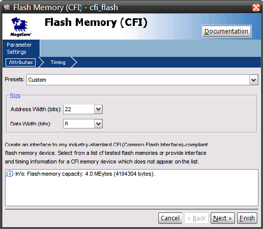
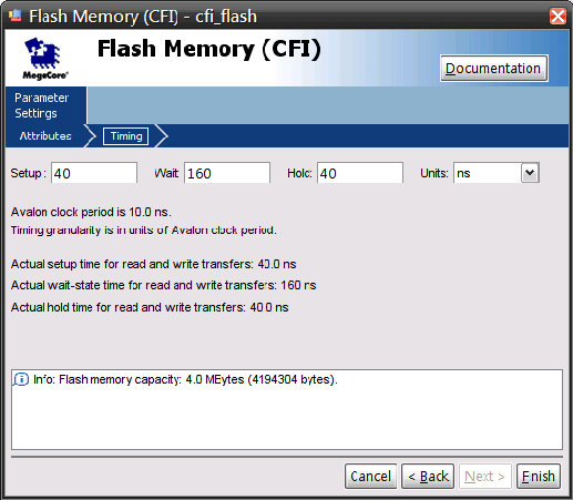
Step 2:
設定Flash Parameter & Timing
Top Module部分
DE2_NIOS_Lite.v / Verilog
2 (C) OOMusou 2008 http://oomusou.cnblogs.com
3
4 Filename : DE2_NIOS_Lite.v
5 Compiler : Quartus II 8.0 + ModelSim-Altera 6.1g
6 Description : DE2_NIOS lite version 1.2
7 Release : 08/08/2008 1.0
8 */
9
10 module DE2_NIOS_Lite (
11 input CLOCK_50, // On Board 50 MHz
12 input [3:0] KEY, // Pushbutton[3:0]
13 input [17:0] SW, // Toggle Switch[17:0]
14 output [8:0] LEDG, // LED Green[8:0]
15 output [17:0] LEDR, // LED Red[17:0]
16 output [6:0] HEX0, // Seven Segment Digit 0
17 output [6:0] HEX1, // Seven Segment Digit 1
18 output [6:0] HEX2, // Seven Segment Digit 2
19 output [6:0] HEX3, // Seven Segment Digit 3
20 output [6:0] HEX4, // Seven Segment Digit 4
21 output [6:0] HEX5, // Seven Segment Digit 5
22 output [6:0] HEX6, // Seven Segment Digit 6
23 output [6:0] HEX7, // Seven Segment Digit 7
24 inout [15:0] DRAM_DQ, // SDRAM Data bus 16 Bits
25 output [11:0] DRAM_ADDR, // SDRAM Address bus 12 Bits
26 output DRAM_LDQM, // SDRAM Low-byte Data Mask
27 output DRAM_UDQM, // SDRAM High-byte Data Mask
28 output DRAM_WE_N, // SDRAM Write Enable
29 output DRAM_CAS_N, // SDRAM Column Address Strobe
30 output DRAM_RAS_N, // SDRAM Row Address Strobe
31 output DRAM_CS_N, // SDRAM Chip Select
32 output DRAM_BA_0, // SDRAM Bank Address 0
33 output DRAM_BA_1, // SDRAM Bank Address 0
34 output DRAM_CLK, // SDRAM Clock
35 output DRAM_CKE, // SDRAM Clock Enable
36 inout [7:0] FL_DQ, // FLASH Data bus 8 Bits
37 output [21:0] FL_ADDR, // FLASH Address bus 22 Bits
38 output FL_WE_N, // FLASH Write Enable
39 output FL_RST_N, // FLASH Reset
40 output FL_OE_N, // FLASH Output Enable
41 output FL_CE_N, // FLASH Chip Enable
42 inout [15:0] SRAM_DQ, // SRAM Data bus 16 Bits
43 output [17:0] SRAM_ADDR, // SRAM Address bus 18 Bits
44 output SRAM_UB_N, // SRAM Low-byte Data Mask
45 output SRAM_LB_N, // SRAM High-byte Data Mask
46 output SRAM_WE_N, // SRAM Write Enable
47 output SRAM_CE_N, // SRAM Chip Enable
48 output SRAM_OE_N // SRAM Output Enable
49 );
50
51 wire CPU_CLK;
52 wire CPU_RESET;
53
54 assign FL_RST_N = 1'b1;
55
56 Reset_Delay u0 (
57 .iRST(KEY[0]),
58 .iCLK(CLOCK_50),
59 .oRESET(CPU_RESET)
60 );
61
62 SDRAM_PLL u1 (
63 .inclk0(CLOCK_50),
64 .c0(DRAM_CLK),
65 .c1(CPU_CLK)
66 );
67
68 nios_ii u2 (
69 .clk(CPU_CLK),
70 .clk_50(CLOCK_50),
71 .reset_n(CPU_RESET),
72 // KEY
73 .in_port_to_the_key_pio(KEY),
74 // SW
75 .in_port_to_the_sw_pio(SW),
76 // LEDG
77 .out_port_from_the_ledg_pio(LEDG),
78 // LEDR
79 .out_port_from_the_ledr_pio(LEDR),
80 // SEG7
81 .oSEG0_from_the_seg7(HEX0),
82 .oSEG1_from_the_seg7(HEX1),
83 .oSEG2_from_the_seg7(HEX2),
84 .oSEG3_from_the_seg7(HEX3),
85 .oSEG4_from_the_seg7(HEX4),
86 .oSEG5_from_the_seg7(HEX5),
87 .oSEG6_from_the_seg7(HEX6),
88 .oSEG7_from_the_seg7(HEX7),
89 // SDRAM
90 .zs_addr_from_the_sdram(DRAM_ADDR),
91 .zs_ba_from_the_sdram({DRAM_BA_1,DRAM_BA_0}),
92 .zs_cas_n_from_the_sdram(DRAM_CAS_N),
93 .zs_cke_from_the_sdram(DRAM_CKE),
94 .zs_cs_n_from_the_sdram(DRAM_CS_N),
95 .zs_dq_to_and_from_the_sdram(DRAM_DQ),
96 .zs_dqm_from_the_sdram({DRAM_UDQM,DRAM_LDQM}),
97 .zs_ras_n_from_the_sdram(DRAM_RAS_N),
98 .zs_we_n_from_the_sdram(DRAM_WE_N),
99 // SRAM
100 .SRAM_ADDR_from_the_sram(SRAM_ADDR),
101 .SRAM_CE_N_from_the_sram(SRAM_CE_N),
102 .SRAM_DQ_to_and_from_the_sram(SRAM_DQ),
103 .SRAM_LB_N_from_the_sram(SRAM_LB_N),
104 .SRAM_OE_N_from_the_sram(SRAM_OE_N),
105 .SRAM_UB_N_from_the_sram(SRAM_UB_N),
106 .SRAM_WE_N_from_the_sram(SRAM_WE_N),
107 // FLASH
108 .address_to_the_cfi_flash(FL_ADDR),
109 .data_to_and_from_the_cfi_flash(FL_DQ),
110 .read_n_to_the_cfi_flash(FL_OE_N),
111 .select_n_to_the_cfi_flash(FL_CE_N),
112 .write_n_to_the_cfi_flash(FL_WE_N)
113 );
114
115 endmodule
107行
.address_to_the_cfi_flash(FL_ADDR),
.data_to_and_from_the_cfi_flash(FL_DQ),
.read_n_to_the_cfi_flash(FL_OE_N),
.select_n_to_the_cfi_flash(FL_CE_N),
.write_n_to_the_cfi_flash(FL_WE_N)
連接SOPC關於flash部分的接腳。
54行
這是大家常忽略的,記得將FL_RST_N設為1'b1。
使用HAL對Flash做讀寫
hello_world.c / C
2 (C) OOMusou 2008 http://oomusou.cnblogs.com
3
4 Filename : hello_world.c
5 Compiler : Nios II EDS 8.0 / ANSI C
6 Description : Demo how to read / write CFI-Flash
7 Release : 10/19/2008 1.0
8 */
9
10 #include <stdio.h>
11 #include "system.h" // CFI_FLASH_NAME
12 #include "sys/alt_flash.h" // flash HAL
13
14 int main() {
15 alt_flash_fd *fd;
16 int i, j, return_code;
17 i = 10;
18 j = 9;
19
20 // open flash
21 fd = alt_flash_open_dev(CFI_FLASH_NAME);
22
23 if (!fd) {
24 printf("alt_flash_open_dev error\n");
25 return -1;
26 }
27
28 // write flash
29 return_code = alt_write_flash(fd, 0, &i, sizeof(int));
30 if (return_code) {
31 printf("alt_write_flash error\n");
32 return -1;
33 }
34
35 // read flash
36 return_code = alt_read_flash(fd, 0, &j, sizeof(int));
37 if (return_code) {
38 printf("alt_read_flash error\n");
39 return -1;
40 }
41
42 // compare input & output
43 if (i == j)
44 printf("i=%d, j=%d, flash read / write OK\n", i, j);
45 else
46 printf("i=%d, j=%d, flash read / write error\n", i, j);
47
48 // close flash
49 alt_flash_close_dev(fd);
50
51 return 0;
52 }
53
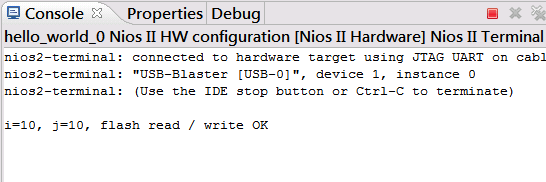
執行結果
11行
#include "sys/alt_flash.h" // flash HAL
system.h記載著SOPC周邊的資訊,sys/alt_flash.h則記載著存取flash的HAL。
20行
fd = alt_flash_open_dev(CFI_FLASH_NAME);
開啟flash。
28行
return_code = alt_write_flash(fd, 0, &i, sizeof(int));
將變數i寫入flash。
35行
return_code = alt_read_flash(fd, 0, &j, sizeof(int));
從flash讀出資料到變數j。
42行
if (i == j)
printf("i=%d, j=%d, flash read / write OK\n", i, j);
else
printf("i=%d, j=%d, flash read / write error\n", i, j);
比較i與j的值是否相等,若相等表示read/write正常。
48行
alt_flash_close_dev(fd);
關閉flash。
完整程式碼下載
DE2_NIOS_Lite_12_flash.7z (for DE2)
DE2_70_NIOS_10_flash.7z (for DE2-70)
Conclusion
事實上Altera還提供了其他對flash存取的HAL,以Quartus II 8.0而言,位於C:\altera\80\nios2eds\components\altera_hal\HAL\inc\sys\alt_flash.h,讀者可自行參考。
DE2-70與DE2類似,就不另外討論,只有SOPC Builder的Flash paramters & timing不太一樣,只提供source code供讀者研究。
See Also
(原創) 如何在Nios II使用Zip File System? (IC Design) (Nios II) (DE2)
(原創) 如何讓Nios II一Power On就執行? (SOC) (Nios II) (SOPC Builder) (DE2) (DE2-70)
(原創) 如何解決No CFI table found at address的錯誤訊息? (SOC) (Nios II) (DE2)
Reference
徐光輝 等著 2006,基於FPGA的嵌入式開發與應用,電子工業出版社

 浙公网安备 33010602011771号