
一、前言
在实时性要求较高的场合中,CPU软件执行的方式显然不能满足需求,这时需要硬件逻辑实现部分功能。要想使自定义IP核被CPU访问,就必须带有总线接口。ZYNQ采用AXI BUS实现PS和PL之间的数据交互。本文以PWM为例设计了自定义AXI总线IP,来演示如何灵活运用ARM+FPGA的架构。
功能定义:在上一篇ZYNQ入门实例博文讲解的系统中添加自定义IP核,其输出驱动LED等实现呼吸灯效果。并且软件通过配置寄存器方式对其进行使能、打开/关闭配置以及选择占空比变化步长。另外,可以按键操作完成占空比变化步长的增减。
平台:米联客 MIZ702N (ZYNQ-7020)
软件:VIVADO+SDK 2017
注:自定义IP逻辑设计采用明德扬至简设计法
二、PWM IP设计
PWM无非就是通过控制周期脉冲信号的占空比,也就是改变高电平在一段固定周期内的持续时间来达到控制目的。脉冲周期需要一个计数器来定时,占空比由低变高和由高变低两种模式同样需要一个计数器来指示,因此这里使用两个嵌套的计数器cnt_cyc和cnt_mode。cnt_mode的加一条件除了要等待cnt_cyc计数完成,还要考虑占空比的变化。
我们可以使用下降沿位置表示占空比,位置越靠近周期值占空比越高。在模式0中下降沿位置按照步长增大直至大于等于周期值,模式1中下降沿位置则按照步长递减直到小于步长。使用两个信号up_stage和down_stage分别指示模式0和模式1。至于步长值,在配置有效时被更新,否则使用默认值。模块最终的输出信号在周期计数器小于下降沿位置为1,反之为零。设计完毕,上代码:


  1 `timescale 1ns / 1ps
  2 //////////////////////////////////////////////////////////////////////////////////
  3 // Company:
  4 // Engineer:
  5 //
  6 // Create Date: 2020/03/01 18:14:44
  7 // Design Name:
  8 // Module Name: pwm
  9 // Project Name:
 10 // Target Devices:
 11 // Tool Versions:
 12 // Description:
 13 //
 14 // Dependencies:
 15 //
 16 // Revision:
 17 // Revision 0.01 - File Created
 18 // Additional Comments:
 19 //
 20 //////////////////////////////////////////////////////////////////////////////////
 21
 22
 23 module pwm(
 24 input                       clk,//频率100MHz 10ns
 25 input                       rst_n,
 26 input                       sw_en,//输出使能
 27 input                       sw_set_en,//步长设定使能
 28 input       [10-1:0]        sw_freq_step,//步长数值
 29 output reg                  led
 30     );
 31
 32 parameter FREQ_STEP = 10'd100;
 33
 34 parameter CNT_CYC_MAX = 50000;
 35
 36 function integer clogb2 (input integer bit_depth);
 37     begin
 38         for(clogb2=0;bit_depth>0;clogb2=clogb2+1)
 39             bit_depth = bit_depth >> 1;
 40     end
 41 endfunction
 42
 43 localparam CNT_CYC_WIDTH = clogb2(CNT_CYC_MAX-1);
 44
 45
 46 reg [CNT_CYC_WIDTH-1:0] cnt_cyc=0;
 47 wire add_cnt_cyc,end_cnt_cyc;
 48 reg [2-1:0] cnt_mode=0;
 49 wire add_cnt_mode,end_cnt_mode;
 50 wire up_stage,down_stage;
 51 reg [CNT_CYC_WIDTH+1-1:0] neg_loc=0;
 52 reg [10-1:0] freq_step=FREQ_STEP;
 53
 54
 55 //周期计数器 计数50ms=50*1000ns = 50000_0ns
 56 always@(posedge clk)begin
 57     if(~rst_n)begin
 58         cnt_cyc <= 0;
 59     end
 60     else if(add_cnt_cyc)begin
 61         if(end_cnt_cyc)
 62             cnt_cyc <= 0;
 63         else
 64             cnt_cyc <= cnt_cyc + 1'b1;
 65     end
 66 end
 67
 68 assign add_cnt_cyc = sw_en == 1;
 69 assign end_cnt_cyc = add_cnt_cyc && cnt_cyc == CNT_CYC_MAX- 1;
 70
 71 //模式计数器 0-占空比递增 1-占空比递减
 72 always@(posedge clk)begin
 73     if(~rst_n)begin
 74         cnt_mode <= 0;
 75     end
 76     else if(add_cnt_mode)begin
 77         if(end_cnt_mode)
 78             cnt_mode <= 0;
 79         else
 80             cnt_mode <= cnt_mode + 1'b1;
 81     end
 82 end
 83
 84 assign add_cnt_mode = end_cnt_cyc && ((up_stage && neg_loc >= CNT_CYC_MAX) || (down_stage && neg_loc == 0));
 85 assign end_cnt_mode = add_cnt_mode && cnt_mode == 2 - 1;
 86
 87
 88 //变化步长设定
 89 always@(posedge clk)begin
 90     if(~rst_n)begin
 91         freq_step <= FREQ_STEP;
 92     end
 93     else if(sw_set_en)begin
 94         if(sw_freq_step >= 1 && sw_freq_step < 2000)
 95             freq_step <= sw_freq_step;
 96         else
 97             freq_step <= FREQ_STEP;
 98     end
 99 end
100
101 //脉冲下降沿对应周期计数器数值
102 always@(posedge clk)begin
103     if(~rst_n)begin
104         neg_loc <= 0;
105     end
106     else if(end_cnt_cyc)begin
107         if(up_stage )begin//占空比递增阶段
108             if(neg_loc < CNT_CYC_MAX)
109                 neg_loc <= neg_loc + freq_step;
110         end
111         else if(down_stage )begin//占空比递减阶段
112             if(neg_loc < freq_step)
113                 neg_loc <= 0;
114             else
115                 neg_loc <= neg_loc - freq_step;
116         end
117     end
118
119 end
120
121 assign up_stage = add_cnt_cyc && cnt_mode == 0;
122 assign down_stage = add_cnt_cyc && cnt_mode == 1;
123
124
125 //输出
126 always@(posedge clk)begin
127     if(~rst_n)begin
128         led <= 1'b0;//高电平点亮
129     end
130     else if(add_cnt_cyc && cnt_cyc < neg_loc)begin
131         led <= 1'b1;
132     end
133     else
134         led <= 1'b0;
135 end
136
137
138
139 endmodule
VIVADO综合、布局布线比较慢,且软硬件级联调试费时费力,所以仿真是极其重要的。编写一个简单的testbench,定义update_freq_step task更新步长。这里使用System Verilog语法有一定的好处。首先单驱动信号可以统一定义为logic变量类型,其次等待时长能指定单位。
 1 `timescale 1ns / 1ps
 2 //////////////////////////////////////////////////////////////////////////////////
 3 // Company:
 4 // Engineer:
 5 //
 6 // Create Date: 2020/03/01 20:49:25
 7 // Design Name:
 8 // Module Name: testbench
 9 // Project Name:
10 // Target Devices:
11 // Tool Versions:
12 // Description:
13 //
14 // Dependencies:
15 //
16 // Revision:
17 // Revision 0.01 - File Created
18 // Additional Comments:
19 //
20 //////////////////////////////////////////////////////////////////////////////////
21
22
23 module testbench();
24
25 logic clk,rst_n;
26 logic sw_en,sw_set_en;
27 logic [10-1:0]sw_freq_step;
28 logic led;
29
30 parameter CYC = 10,
31           RST_TIM = 2;
32
33 defparam dut.CNT_CYC_MAX = 2000;
34
35  pwm#(.FREQ_STEP(100))
36  dut(
37 .clk           (clk) ,//频率100MHz 10ns
38 .rst_n         (rst_n) ,
39 .sw_en         (sw_en) ,//输出使能
40 .sw_set_en     (sw_set_en) ,//步长设定使能
41 .sw_freq_step  (sw_freq_step) ,//步长数值
42 .led           (led)
43     );
44
45 initial begin
46     clk = 1;
47     forever begin
48         #(CYC/2.0);
49         clk=~clk;
50     end
51 end
52
53 initial begin
54     rst_n = 1;
55     #1;
56     rst_n = 0;
57     #(RST_TIM*CYC) rst_n = 1;
58 end
59
60 initial begin
61     sw_en = 0;
62     sw_set_en = 0;
63     sw_freq_step = 'd10;
64     #1;
65     #(RST_TIM*CYC);
66     #(CYC*10);
67     sw_en = 1;
68
69     #600us;
70     update_freq_step(50);
71     #600us;
72     $stop;
73
74 end
75
76 task update_freq_step([10-1:0] freq_step);
77     sw_set_en = 1;
78     sw_freq_step = freq_step;
79     #(1*CYC);
80     sw_set_en = 0;
81 endtask
82
83 endmodule
设计较简单,直接使用VIVADO仿真器观察波形即可:
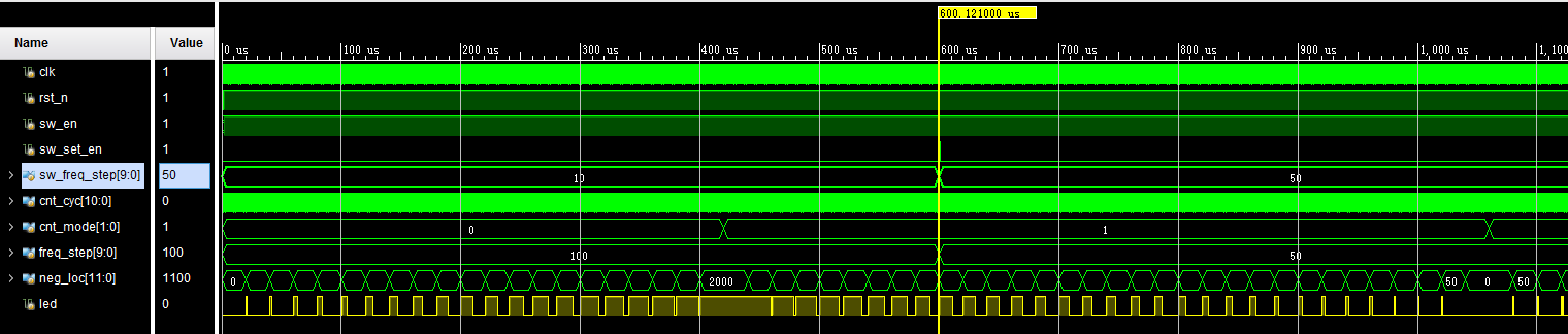
可以看到输出信号led的占空比在不断起伏变化,当更新freq_step为50后变化更为减慢。
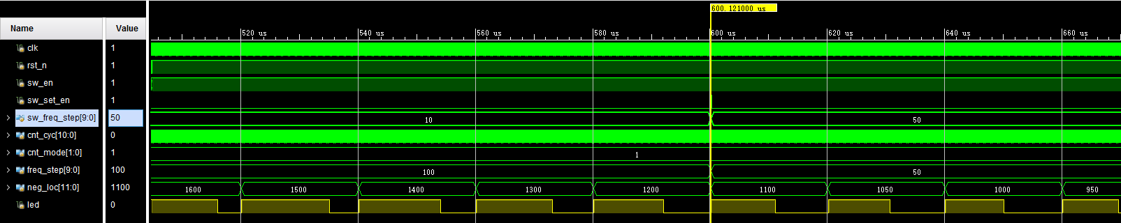
配置前相邻两个neg_loc数值差与更新后分别是100和50。以上证明逻辑功能无误。
三、硬件系统搭建
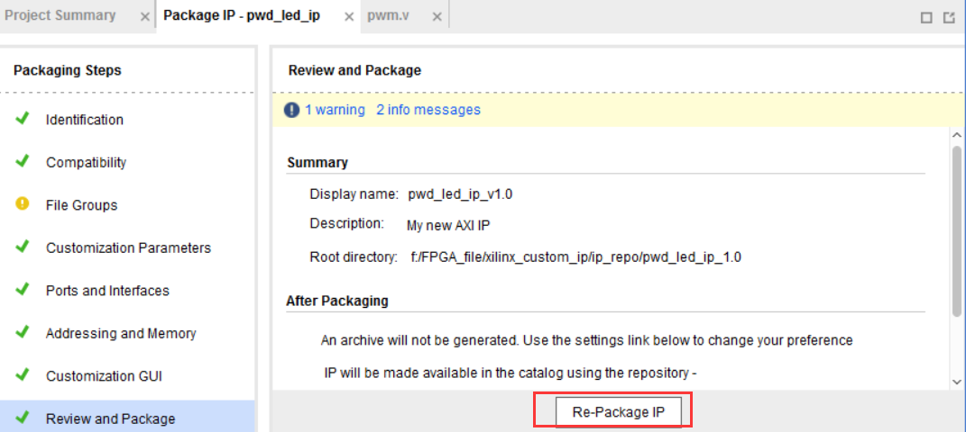
设计完PWM功能模块还没有完,需要再包一层总线Wrapper才能被CPU访问。创建AXI总线IP
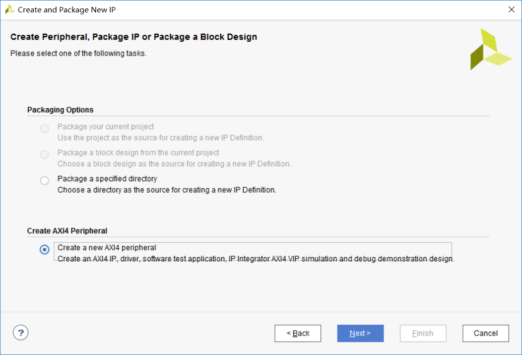
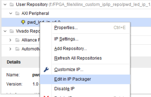
在封装器中编辑。
最终IP结构如图:

具体操作不过多讲述,直接以代码呈现:
 1 `timescale 1 ns / 1 ps
 2
 3     module pwm_led_ip_v1_0 #
 4     (
 5         // Users to add parameters here
 6         parameter FREQ_STEP = 10'd100,
 7         // User parameters ends
 8         // Do not modify the parameters beyond this line
 9
10
11         // Parameters of Axi Slave Bus Interface S00_AXI
12         parameter integer C_S00_AXI_DATA_WIDTH    = 32,
13         parameter integer C_S00_AXI_ADDR_WIDTH    = 4
14     )
15     (
16         // Users to add ports here
17         output led,
18         // User ports ends
19         // Do not modify the ports beyond this line
20
21
22         // Ports of Axi Slave Bus Interface S00_AXI
23         input wire  s00_axi_aclk,
24         input wire  s00_axi_aresetn,
25         input wire [C_S00_AXI_ADDR_WIDTH-1 : 0] s00_axi_awaddr,
26         input wire [2 : 0] s00_axi_awprot,
27         input wire  s00_axi_awvalid,
28         output wire  s00_axi_awready,
29         input wire [C_S00_AXI_DATA_WIDTH-1 : 0] s00_axi_wdata,
30         input wire [(C_S00_AXI_DATA_WIDTH/8)-1 : 0] s00_axi_wstrb,
31         input wire  s00_axi_wvalid,
32         output wire  s00_axi_wready,
33         output wire [1 : 0] s00_axi_bresp,
34         output wire  s00_axi_bvalid,
35         input wire  s00_axi_bready,
36         input wire [C_S00_AXI_ADDR_WIDTH-1 : 0] s00_axi_araddr,
37         input wire [2 : 0] s00_axi_arprot,
38         input wire  s00_axi_arvalid,
39         output wire  s00_axi_arready,
40         output wire [C_S00_AXI_DATA_WIDTH-1 : 0] s00_axi_rdata,
41         output wire [1 : 0] s00_axi_rresp,
42         output wire  s00_axi_rvalid,
43         input wire  s00_axi_rready
44     );
45 // Instantiation of Axi Bus Interface S00_AXI
46     pwd_led_ip_v1_0_S00_AXI # (
47         .C_S_AXI_DATA_WIDTH(C_S00_AXI_DATA_WIDTH),
48         .C_S_AXI_ADDR_WIDTH(C_S00_AXI_ADDR_WIDTH),
49         .FREQ_STEP(FREQ_STEP)
50     ) pwd_led_ip_v1_0_S00_AXI_inst (
51         .S_AXI_ACLK(s00_axi_aclk),
52         .S_AXI_ARESETN(s00_axi_aresetn),
53         .S_AXI_AWADDR(s00_axi_awaddr),
54         .S_AXI_AWPROT(s00_axi_awprot),
55         .S_AXI_AWVALID(s00_axi_awvalid),
56         .S_AXI_AWREADY(s00_axi_awready),
57         .S_AXI_WDATA(s00_axi_wdata),
58         .S_AXI_WSTRB(s00_axi_wstrb),
59         .S_AXI_WVALID(s00_axi_wvalid),
60         .S_AXI_WREADY(s00_axi_wready),
61         .S_AXI_BRESP(s00_axi_bresp),
62         .S_AXI_BVALID(s00_axi_bvalid),
63         .S_AXI_BREADY(s00_axi_bready),
64         .S_AXI_ARADDR(s00_axi_araddr),
65         .S_AXI_ARPROT(s00_axi_arprot),
66         .S_AXI_ARVALID(s00_axi_arvalid),
67         .S_AXI_ARREADY(s00_axi_arready),
68         .S_AXI_RDATA(s00_axi_rdata),
69         .S_AXI_RRESP(s00_axi_rresp),
70         .S_AXI_RVALID(s00_axi_rvalid),
71         .S_AXI_RREADY(s00_axi_rready),
72
73         .led(led)
74     );
75
76     // Add user logic here
77
78     // User logic ends
79
80     endmodule
  1 `timescale 1 ns / 1 ps
  2
  3     module pwm_led_ip_v1_0_S00_AXI #
  4     (
  5         // Users to add parameters here
  6         parameter FREQ_STEP = 10'd100,
  7         // User parameters ends
  8         // Do not modify the parameters beyond this line
  9
 10         // Width of S_AXI data bus
 11         parameter integer C_S_AXI_DATA_WIDTH    = 32,
 12         // Width of S_AXI address bus
 13         parameter integer C_S_AXI_ADDR_WIDTH    = 4
 14     )
 15     (
 16         // Users to add ports here
 17         output led,
 18         // User ports ends
 19         // Do not modify the ports beyond this line
 20
 21         // Global Clock Signal
 22         input wire  S_AXI_ACLK,
 23         // Global Reset Signal. This Signal is Active LOW
 24         input wire  S_AXI_ARESETN,
 25         // Write address (issued by master, acceped by Slave)
 26         input wire [C_S_AXI_ADDR_WIDTH-1 : 0] S_AXI_AWADDR,
 27         // Write channel Protection type. This signal indicates the
 28             // privilege and security level of the transaction, and whether
 29             // the transaction is a data access or an instruction access.
 30         input wire [2 : 0] S_AXI_AWPROT,
 31         // Write address valid. This signal indicates that the master signaling
 32             // valid write address and control information.
 33         input wire  S_AXI_AWVALID,
 34         // Write address ready. This signal indicates that the slave is ready
 35             // to accept an address and associated control signals.
 36         output wire  S_AXI_AWREADY,
 37         // Write data (issued by master, acceped by Slave)
 38         input wire [C_S_AXI_DATA_WIDTH-1 : 0] S_AXI_WDATA,
 39         // Write strobes. This signal indicates which byte lanes hold
 40             // valid data. There is one write strobe bit for each eight
 41             // bits of the write data bus.
 42         input wire [(C_S_AXI_DATA_WIDTH/8)-1 : 0] S_AXI_WSTRB,
 43         // Write valid. This signal indicates that valid write
 44             // data and strobes are available.
 45         input wire  S_AXI_WVALID,
 46         // Write ready. This signal indicates that the slave
 47             // can accept the write data.
 48         output wire  S_AXI_WREADY,
 49         // Write response. This signal indicates the status
 50             // of the write transaction.
 51         output wire [1 : 0] S_AXI_BRESP,
 52         // Write response valid. This signal indicates that the channel
 53             // is signaling a valid write response.
 54         output wire  S_AXI_BVALID,
 55         // Response ready. This signal indicates that the master
 56             // can accept a write response.
 57         input wire  S_AXI_BREADY,
 58         // Read address (issued by master, acceped by Slave)
 59         input wire [C_S_AXI_ADDR_WIDTH-1 : 0] S_AXI_ARADDR,
 60         // Protection type. This signal indicates the privilege
 61             // and security level of the transaction, and whether the
 62             // transaction is a data access or an instruction access.
 63         input wire [2 : 0] S_AXI_ARPROT,
 64         // Read address valid. This signal indicates that the channel
 65             // is signaling valid read address and control information.
 66         input wire  S_AXI_ARVALID,
 67         // Read address ready. This signal indicates that the slave is
 68             // ready to accept an address and associated control signals.
 69         output wire  S_AXI_ARREADY,
 70         // Read data (issued by slave)
 71         output wire [C_S_AXI_DATA_WIDTH-1 : 0] S_AXI_RDATA,
 72         // Read response. This signal indicates the status of the
 73             // read transfer.
 74         output wire [1 : 0] S_AXI_RRESP,
 75         // Read valid. This signal indicates that the channel is
 76             // signaling the required read data.
 77         output wire  S_AXI_RVALID,
 78         // Read ready. This signal indicates that the master can
 79             // accept the read data and response information.
 80         input wire  S_AXI_RREADY
 81     );
 82
 83     // AXI4LITE signals
 84     reg [C_S_AXI_ADDR_WIDTH-1 : 0]     axi_awaddr;
 85     reg      axi_awready;
 86     reg      axi_wready;
 87     reg [1 : 0]     axi_bresp;
 88     reg      axi_bvalid;
 89     reg [C_S_AXI_ADDR_WIDTH-1 : 0]     axi_araddr;
 90     reg      axi_arready;
 91     reg [C_S_AXI_DATA_WIDTH-1 : 0]     axi_rdata;
 92     reg [1 : 0]     axi_rresp;
 93     reg      axi_rvalid;
 94
 95     // Example-specific design signals
 96     // local parameter for addressing 32 bit / 64 bit C_S_AXI_DATA_WIDTH
 97     // ADDR_LSB is used for addressing 32/64 bit registers/memories
 98     // ADDR_LSB = 2 for 32 bits (n downto 2)
 99     // ADDR_LSB = 3 for 64 bits (n downto 3)
100     localparam integer ADDR_LSB = (C_S_AXI_DATA_WIDTH/32) + 1;
101     localparam integer OPT_MEM_ADDR_BITS = 1;
102     //----------------------------------------------
103     //-- Signals for user logic register space example
104     //------------------------------------------------
105     //-- Number of Slave Registers 4
106     reg [C_S_AXI_DATA_WIDTH-1:0]    slv_reg0;
107     reg [C_S_AXI_DATA_WIDTH-1:0]    slv_reg1;
108     reg [C_S_AXI_DATA_WIDTH-1:0]    slv_reg2;
109     reg [C_S_AXI_DATA_WIDTH-1:0]    slv_reg3;
110     wire     slv_reg_rden;
111     wire     slv_reg_wren;
112     reg [C_S_AXI_DATA_WIDTH-1:0]     reg_data_out;
113     integer     byte_index;
114     reg     aw_en;
115
116     // I/O Connections assignments
117
118     assign S_AXI_AWREADY    = axi_awready;
119     assign S_AXI_WREADY    = axi_wready;
120     assign S_AXI_BRESP    = axi_bresp;
121     assign S_AXI_BVALID    = axi_bvalid;
122     assign S_AXI_ARREADY    = axi_arready;
123     assign S_AXI_RDATA    = axi_rdata;
124     assign S_AXI_RRESP    = axi_rresp;
125     assign S_AXI_RVALID    = axi_rvalid;
126     // Implement axi_awready generation
127     // axi_awready is asserted for one S_AXI_ACLK clock cycle when both
128     // S_AXI_AWVALID and S_AXI_WVALID are asserted. axi_awready is
129     // de-asserted when reset is low.
130
131     always @( posedge S_AXI_ACLK )
132     begin
133       if ( S_AXI_ARESETN == 1'b0 )
134         begin
135           axi_awready <= 1'b0;
136           aw_en <= 1'b1;
137         end
138       else
139         begin
140           if (~axi_awready && S_AXI_AWVALID && S_AXI_WVALID && aw_en)
141             begin
142               // slave is ready to accept write address when
143               // there is a valid write address and write data
144               // on the write address and data bus. This design
145               // expects no outstanding transactions.
146               axi_awready <= 1'b1;
147               aw_en <= 1'b0;
148             end
149             else if (S_AXI_BREADY && axi_bvalid)
150                 begin
151                   aw_en <= 1'b1;
152                   axi_awready <= 1'b0;
153                 end
154           else
155             begin
156               axi_awready <= 1'b0;
157             end
158         end
159     end
160
161     // Implement axi_awaddr latching
162     // This process is used to latch the address when both
163     // S_AXI_AWVALID and S_AXI_WVALID are valid.
164
165     always @( posedge S_AXI_ACLK )
166     begin
167       if ( S_AXI_ARESETN == 1'b0 )
168         begin
169           axi_awaddr <= 0;
170         end
171       else
172         begin
173           if (~axi_awready && S_AXI_AWVALID && S_AXI_WVALID && aw_en)
174             begin
175               // Write Address latching
176               axi_awaddr <= S_AXI_AWADDR;
177             end
178         end
179     end
180
181     // Implement axi_wready generation
182     // axi_wready is asserted for one S_AXI_ACLK clock cycle when both
183     // S_AXI_AWVALID and S_AXI_WVALID are asserted. axi_wready is
184     // de-asserted when reset is low.
185
186     always @( posedge S_AXI_ACLK )
187     begin
188       if ( S_AXI_ARESETN == 1'b0 )
189         begin
190           axi_wready <= 1'b0;
191         end
192       else
193         begin
194           if (~axi_wready && S_AXI_WVALID && S_AXI_AWVALID && aw_en )
195             begin
196               // slave is ready to accept write data when
197               // there is a valid write address and write data
198               // on the write address and data bus. This design
199               // expects no outstanding transactions.
200               axi_wready <= 1'b1;
201             end
202           else
203             begin
204               axi_wready <= 1'b0;
205             end
206         end
207     end
208
209     // Implement memory mapped register select and write logic generation
210     // The write data is accepted and written to memory mapped registers when
211     // axi_awready, S_AXI_WVALID, axi_wready and S_AXI_WVALID are asserted. Write strobes are used to
212     // select byte enables of slave registers while writing.
213     // These registers are cleared when reset (active low) is applied.
214     // Slave register write enable is asserted when valid address and data are available
215     // and the slave is ready to accept the write address and write data.
216     assign slv_reg_wren = axi_wready && S_AXI_WVALID && axi_awready && S_AXI_AWVALID;
217
218     always @( posedge S_AXI_ACLK )
219     begin
220       if ( S_AXI_ARESETN == 1'b0 )
221         begin
222           slv_reg0 <= 0;
223           slv_reg1 <= 0;
224           slv_reg2 <= 0;
225           slv_reg3 <= 0;
226         end
227       else begin
228         if (slv_reg_wren)
229           begin
230             case ( axi_awaddr[ADDR_LSB+OPT_MEM_ADDR_BITS:ADDR_LSB] )
231               2'h0:
232                 for ( byte_index = 0; byte_index <= (C_S_AXI_DATA_WIDTH/8)-1; byte_index = byte_index+1 )
233                   if ( S_AXI_WSTRB[byte_index] == 1 ) begin
234                     // Respective byte enables are asserted as per write strobes
235                     // Slave register 0
236                     slv_reg0[(byte_index*8) +: 8] <= S_AXI_WDATA[(byte_index*8) +: 8];
237                   end
238               2'h1:
239                 for ( byte_index = 0; byte_index <= (C_S_AXI_DATA_WIDTH/8)-1; byte_index = byte_index+1 )
240                   if ( S_AXI_WSTRB[byte_index] == 1 ) begin
241                     // Respective byte enables are asserted as per write strobes
242                     // Slave register 1
243                     slv_reg1[(byte_index*8) +: 8] <= S_AXI_WDATA[(byte_index*8) +: 8];
244                   end
245               2'h2:
246                 for ( byte_index = 0; byte_index <= (C_S_AXI_DATA_WIDTH/8)-1; byte_index = byte_index+1 )
247                   if ( S_AXI_WSTRB[byte_index] == 1 ) begin
248                     // Respective byte enables are asserted as per write strobes
249                     // Slave register 2
250                     slv_reg2[(byte_index*8) +: 8] <= S_AXI_WDATA[(byte_index*8) +: 8];
251                   end
252               2'h3:
253                 for ( byte_index = 0; byte_index <= (C_S_AXI_DATA_WIDTH/8)-1; byte_index = byte_index+1 )
254                   if ( S_AXI_WSTRB[byte_index] == 1 ) begin
255                     // Respective byte enables are asserted as per write strobes
256                     // Slave register 3
257                     slv_reg3[(byte_index*8) +: 8] <= S_AXI_WDATA[(byte_index*8) +: 8];
258                   end
259               default : begin
260                           slv_reg0 <= slv_reg0;
261                           slv_reg1 <= slv_reg1;
262                           slv_reg2 <= slv_reg2;
263                           slv_reg3 <= slv_reg3;
264                         end
265             endcase
266           end
267       end
268     end
269
270     // Implement write response logic generation
271     // The write response and response valid signals are asserted by the slave
272     // when axi_wready, S_AXI_WVALID, axi_wready and S_AXI_WVALID are asserted.
273     // This marks the acceptance of address and indicates the status of
274     // write transaction.
275
276     always @( posedge S_AXI_ACLK )
277     begin
278       if ( S_AXI_ARESETN == 1'b0 )
279         begin
280           axi_bvalid  <= 0;
281           axi_bresp   <= 2'b0;
282         end
283       else
284         begin
285           if (axi_awready && S_AXI_AWVALID && ~axi_bvalid && axi_wready && S_AXI_WVALID)
286             begin
287               // indicates a valid write response is available
288               axi_bvalid <= 1'b1;
289               axi_bresp  <= 2'b0; // 'OKAY' response
290             end                   // work error responses in future
291           else
292             begin
293               if (S_AXI_BREADY && axi_bvalid)
294                 //check if bready is asserted while bvalid is high)
295                 //(there is a possibility that bready is always asserted high)
296                 begin
297                   axi_bvalid <= 1'b0;
298                 end
299             end
300         end
301     end
302
303     // Implement axi_arready generation
304     // axi_arready is asserted for one S_AXI_ACLK clock cycle when
305     // S_AXI_ARVALID is asserted. axi_awready is
306     // de-asserted when reset (active low) is asserted.
307     // The read address is also latched when S_AXI_ARVALID is
308     // asserted. axi_araddr is reset to zero on reset assertion.
309
310     always @( posedge S_AXI_ACLK )
311     begin
312       if ( S_AXI_ARESETN == 1'b0 )
313         begin
314           axi_arready <= 1'b0;
315           axi_araddr  <= 32'b0;
316         end
317       else
318         begin
319           if (~axi_arready && S_AXI_ARVALID)
320             begin
321               // indicates that the slave has acceped the valid read address
322               axi_arready <= 1'b1;
323               // Read address latching
324               axi_araddr  <= S_AXI_ARADDR;
325             end
326           else
327             begin
328               axi_arready <= 1'b0;
329             end
330         end
331     end
332
333     // Implement axi_arvalid generation
334     // axi_rvalid is asserted for one S_AXI_ACLK clock cycle when both
335     // S_AXI_ARVALID and axi_arready are asserted. The slave registers
336     // data are available on the axi_rdata bus at this instance. The
337     // assertion of axi_rvalid marks the validity of read data on the
338     // bus and axi_rresp indicates the status of read transaction.axi_rvalid
339     // is deasserted on reset (active low). axi_rresp and axi_rdata are
340     // cleared to zero on reset (active low).
341     always @( posedge S_AXI_ACLK )
342     begin
343       if ( S_AXI_ARESETN == 1'b0 )
344         begin
345           axi_rvalid <= 0;
346           axi_rresp  <= 0;
347         end
348       else
349         begin
350           if (axi_arready && S_AXI_ARVALID && ~axi_rvalid)
351             begin
352               // Valid read data is available at the read data bus
353               axi_rvalid <= 1'b1;
354               axi_rresp  <= 2'b0; // 'OKAY' response
355             end
356           else if (axi_rvalid && S_AXI_RREADY)
357             begin
358               // Read data is accepted by the master
359               axi_rvalid <= 1'b0;
360             end
361         end
362     end
363
364     // Implement memory mapped register select and read logic generation
365     // Slave register read enable is asserted when valid address is available
366     // and the slave is ready to accept the read address.
367     assign slv_reg_rden = axi_arready & S_AXI_ARVALID & ~axi_rvalid;
368     always @(*)
369     begin
370           // Address decoding for reading registers
371           case ( axi_araddr[ADDR_LSB+OPT_MEM_ADDR_BITS:ADDR_LSB] )
372             2'h0   : reg_data_out <= slv_reg0;
373             2'h1   : reg_data_out <= slv_reg1;
374             2'h2   : reg_data_out <= slv_reg2;
375             2'h3   : reg_data_out <= slv_reg3;
376             default : reg_data_out <= 0;
377           endcase
378     end
379
380     // Output register or memory read data
381     always @( posedge S_AXI_ACLK )
382     begin
383       if ( S_AXI_ARESETN == 1'b0 )
384         begin
385           axi_rdata  <= 0;
386         end
387       else
388         begin
389           // When there is a valid read address (S_AXI_ARVALID) with
390           // acceptance of read address by the slave (axi_arready),
391           // output the read dada
392           if (slv_reg_rden)
393             begin
394               axi_rdata <= reg_data_out;     // register read data
395             end
396         end
397     end
398
399     // Add user logic here
400     pwm#(.FREQ_STEP(FREQ_STEP))
401     u_pwm(
402     .clk            (S_AXI_ACLK),
403     .rst_n          (S_AXI_ARESETN),
404     .sw_en          (slv_reg0[0]),
405     .sw_set_en      (slv_reg1[0]),
406     .sw_freq_step   (slv_reg2[10-1:0]),
407     .led            (led)
408     );
409     // User logic ends
410
411     endmodule
最后重新封装
接下来搭建硬件IP子系统。
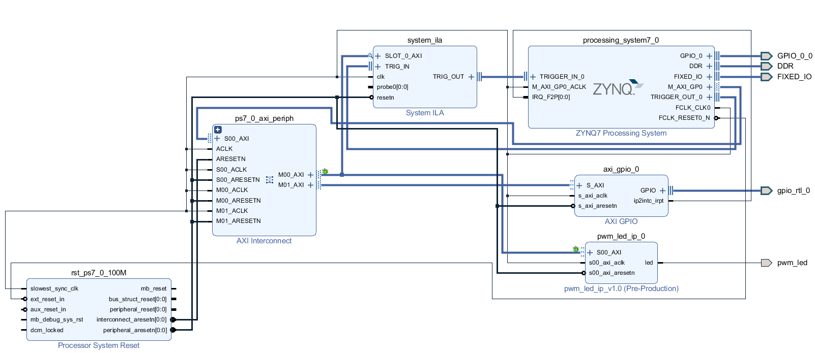
和之前相比只是添加了pwm_led_ip_0,并连接在AXI Interconnect的另一个Master接口上。使用SystemILA抓取总线信号以备后续观察。还是同样的操作流程:生成输出文件,生成HDL Wrapper,添加管脚约束文件,综合,实现,生成比特流并导出硬件,启动SDK软件环境。
四、软件编程与调试
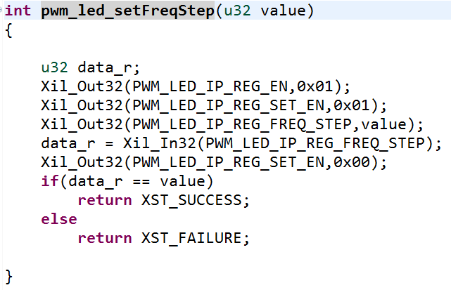
其实CPU控制自定义IP的方式就是读写数据,写就是对指针赋值,读就是返回指针所指向地址中的数据,分别使用Xil_Out32()和Xil_In32()实现。创建pwm_led_ip.h文件,进行地址宏定义并编写配置函数。为了更好地实现软件库的封装和扩展,创建environment.h文件来include不同的库以及宏定义、全局变量定义。
软件代码如下:
  1 /*
  2  * main.c
  3  *
  4  *  Created on: 2020年2月22日
  5  *      Author: s
  6  */
  7
  8
  9 #include "environment.h"
 10
 11 void GpioHandler(void *CallbackRef);
 12 int setupIntSystem(XScuGic *IntcInstancePtr,XGpio *gpioInstancePtr
 13         ,u32 IntrId);
 14
 15 int main()
 16 {
 17     int Status;
 18     u8 i=0;
 19     u32 sys_led_out=0x1;
 20     u32 data_r;
 21     freq_step_value = 10;
 22
 23     Status = gpiops_initialize(&GpioPs,GPIOPS_DEVICE_ID);
 24     if (Status != XST_SUCCESS) {
 25         return XST_FAILURE;
 26     }
 27
 28     Status = gpio_initialize(&Gpio,GPIO_DEVICE_ID);
 29     if (Status != XST_SUCCESS) {
 30         return XST_FAILURE;
 31     }
 32
 33     /*
 34      * Set the direction for the pin to be output and
 35     * Enable the Output enable for the LED Pin.
 36      */
 37     gpiops_setOutput(&GpioPs,MIO_OUT_PIN_INDEX);
 38
 39     for(i=0;i<LOOP_NUM;i++){
 40         gpiops_setOutput(&GpioPs,EMIO_OUT_PIN_BASE_INDEX+i);
 41     }
 42
 43     gpio_setDirect(&Gpio, 1,GPIO_CHANNEL1);
 44
 45     Status = setupIntSystem(&Intc,&Gpio,INTC_GPIO_INTERRUPT_ID);
 46     if (Status != XST_SUCCESS) {
 47             return XST_FAILURE;
 48         }
 49
 50     Status = pwm_led_setFreqStep(freq_step_value);
 51     if (Status != XST_SUCCESS) {
 52             return XST_FAILURE;
 53         }
 54
 55     printf("Initialization finish.\n");
 56
 57     while(1){
 58
 59         for(i=0;i<LOOP_NUM;i++){
 60             if(int_flag == 0)
 61             {
 62                 gpiops_outputValue(&GpioPs, EMIO_OUT_PIN_BASE_INDEX+i, 0x1);
 63                 usleep(200*1000);
 64                 gpiops_outputValue(&GpioPs, EMIO_OUT_PIN_BASE_INDEX+i, 0x0);
 65             }
 66             else
 67             {
 68                 gpiops_outputValue(&GpioPs, EMIO_OUT_PIN_BASE_INDEX+LOOP_NUM-1-i, 0x1);
 69                 usleep(200*1000);
 70                 gpiops_outputValue(&GpioPs, EMIO_OUT_PIN_BASE_INDEX+LOOP_NUM-1-i, 0x0);
 71             }
 72         }
 73
 74         gpiops_outputValue(&GpioPs, MIO_OUT_PIN_INDEX, sys_led_out);
 75         sys_led_out  = sys_led_out == 0x0 ? 0x1 : 0x0;
 76     }
 77     return 0;
 78 }
 79
 80
 81
 82 int setupIntSystem(XScuGic *IntcInstancePtr,XGpio *gpioInstancePtr
 83         ,u32 IntrId)
 84 {
 85     int Result;
 86     /*
 87     * Initialize the interrupt controller driver so that it is ready to
 88     * use.
 89     */
 90
 91     Result = gic_initialize(&Intc,INTC_DEVICE_ID);
 92     if (Result != XST_SUCCESS) {
 93             return XST_FAILURE;
 94         }
 95
 96     XScuGic_SetPriorityTriggerType(IntcInstancePtr, IntrId,
 97                         0xA0, 0x3);
 98
 99     /*
100     * Connect the interrupt handler that will be called when an
101      * interrupt occurs for the device.
102      */
103     Result = XScuGic_Connect(IntcInstancePtr, IntrId,
104                 (Xil_ExceptionHandler)GpioHandler, gpioInstancePtr);
105     if (Result != XST_SUCCESS) {
106         return Result;
107     }
108
109     /* Enable the interrupt for the GPIO device.*/
110     XScuGic_Enable(IntcInstancePtr, IntrId);
111
112     /*
113      * Enable the GPIO channel interrupts so that push button can be
114     * detected and enable interrupts for the GPIO device
115     */
116     XGpio_InterruptEnable(gpioInstancePtr,GPIO_CHANNEL1);
117     XGpio_InterruptGlobalEnable(gpioInstancePtr);
118
119     /*
120     * Initialize the exception table and register the interrupt
121     * controller handler with the exception table
122     */
123     exception_enable(&Intc);
124
125     IntrFlag = 0;
126
127     return XST_SUCCESS;
128 }
129
130 void GpioHandler(void *CallbackRef)
131 {
132     XGpio *GpioPtr = (XGpio *)CallbackRef;
133     u32 gpio_inputValue;
134
135
136     /* Clear the Interrupt */
137     XGpio_InterruptClear(GpioPtr, GPIO_CHANNEL1);
138     printf("Input interrupt routine.\n");
139
140     //IntrFlag = 1;
141     gpio_inputValue = gpio_readValue(GpioPtr, 1);
142     switch(gpio_inputValue)
143     {
144     case 30:
145         //printf("button up\n");
146         freq_step_value+=10;
147         pwm_led_setFreqStep(freq_step_value);
148         break;
149     case 29:
150         printf("button center\n");
151         break;
152     case 27:
153         //printf("button left\n");
154         int_flag = 0;
155         break;
156     case 23:
157         //printf("button right\n");
158         int_flag = 1;
159         break;
160     case 15:
161         //print("button down\n");
162         freq_step_value-=10;
163         pwm_led_setFreqStep(freq_step_value);
164         break;
165     }
166
167 }
 1 /*
 2  * environment.h
 3  *
 4  *  Created on: 2020年3月2日
 5  *      Author: s
 6  */
 7
 8 #ifndef SRC_ENVIRONMENT_H_
 9 #define SRC_ENVIRONMENT_H_
10
11 #include "xparameters.h"
12 #include <xil_printf.h>
13 #include "sleep.h"
14 #include "xstatus.h"
15
16 #include "gpiops.h"
17 #include "gpio.h"
18 #include "pwm_led_ip.h"
19 #include "gic.h"
20
21 XGpioPs GpioPs;    /* The driver instance for GPIO Device. */
22 XGpio Gpio;
23 XScuGic Intc; /* The Instance of the Interrupt Controller Driver */
24
25
26
27 #define printf            xil_printf    /* Smalller foot-print printf */
28 #define LOOP_NUM 4
29
30
31 u32 MIO_OUT_PIN_INDEX =7; /* LED button */
32 u32 EMIO_OUT_PIN_BASE_INDEX = 54;
33 volatile u32 IntrFlag; /* Interrupt Handler Flag */
34
35 #endif /* SRC_ENVIRONMENT_H_ */
 1 /*
 2  * pwm_led_ip.h
 3  *
 4  *  Created on: 2020年3月2日
 5  *      Author: s
 6  */
 7
 8 #ifndef SRC_PWM_LED_IP_H_
 9 #define SRC_PWM_LED_IP_H_
10
11 #define PWM_LED_IP_S00_AXI_SLV_REG0_OFFSET 0
12 #define PWM_LED_IP_S00_AXI_SLV_REG1_OFFSET 4
13 #define PWM_LED_IP_S00_AXI_SLV_REG2_OFFSET 8
14 #define PWM_LED_IP_S00_AXI_SLV_REG3_OFFSET 12
15
16 #define PWM_LED_IP_BASEADDR XPAR_PWM_LED_IP_0_S00_AXI_BASEADDR
17 #define FREQ_STEP_SET_VALUE 30
18
19 #define PWM_LED_IP_REG_EN (PWM_LED_IP_BASEADDR+PWM_LED_IP_S00_AXI_SLV_REG0_OFFSET)
20 #define PWM_LED_IP_REG_SET_EN (PWM_LED_IP_BASEADDR+PWM_LED_IP_S00_AXI_SLV_REG1_OFFSET)
21 #define PWM_LED_IP_REG_FREQ_STEP (PWM_LED_IP_BASEADDR+PWM_LED_IP_S00_AXI_SLV_REG2_OFFSET)
22 #define PWM_LED_IP_REG_RESERVED (PWM_LED_IP_BASEADDR+PWM_LED_IP_S00_AXI_SLV_REG3_OFFSET)
23
24 volatile u32 freq_step_value;
25
26 int pwm_led_setFreqStep(u32 value)
27 {
28
29     u32 data_r;
30     Xil_Out32(PWM_LED_IP_REG_EN,0x01);
31     Xil_Out32(PWM_LED_IP_REG_SET_EN,0x01);
32     Xil_Out32(PWM_LED_IP_REG_FREQ_STEP,value);
33     data_r = Xil_In32(PWM_LED_IP_REG_FREQ_STEP);
34     Xil_Out32(PWM_LED_IP_REG_SET_EN,0x00);
35     if(data_r == value)
36         return XST_SUCCESS;
37     else
38         return XST_FAILURE;
39
40 }
41
42 #endif /* SRC_PWM_LED_IP_H_ */
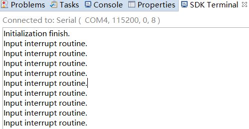
其他文件与上一篇ZYNQ入门实例博文相同。Run程序后多次按下按键,从串口terminal可以看出系统初始化成功,进入按键中断回调函数。开发板上呼吸灯频率也随着按键按下在变化。
最后打开VIVADO硬件管理器,观察AXI总线波形: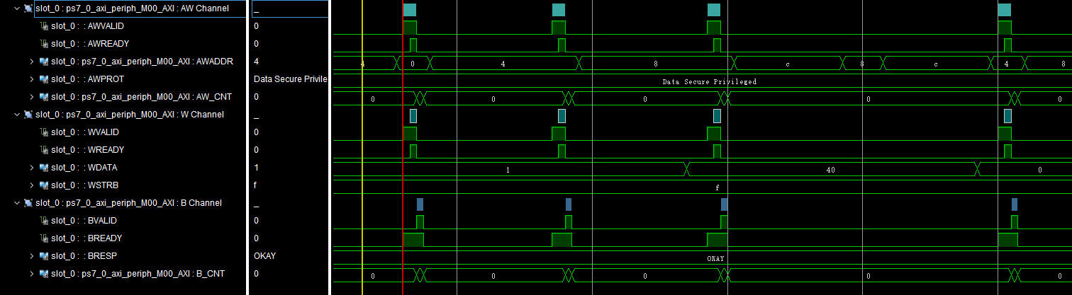
按下步长值增加按键后,会有四次写数据操作,正好对应pwm_led_setFreqStep function中的四次Xil_Out32调用。每次写后一个时钟周期写响应通道BVALID拉高一个时钟周期证明写正确。
再来观察用于确认写入无误的读操作对应总线波形:
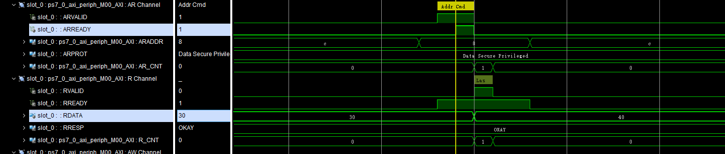
读取数据为40,与写入一致。到此功能定义、设计规划、硬件逻辑设计仿真、IP封装、子系统搭建、软件设计、板级调试的流程全部走完。

 浙公网安备 33010602011771号