经典论文《异步FIFO设计的仿真与综合技术》双语研读
Simulation and Synthesis Techniques for Asynchronous FIFO Design
作者:Clifford E. Cummings,Sunburst Design,Inc,Cliffc@sunburst-design.com
今天对跨时钟域FIFO设计领域的经典论文进行双语研读,力求还原原汁原味。
摘要
1.0 引言
An asynchronous FIFO refers to a FIFO design where data values are written to a FIFO buffer from one clock domain and the data values are read from the same FIFO buffer from another clock domain, where the two clock domains are asynchronous to each other.Asynchronous FIFOs are used to safely pass data from one clock domain to another clock domain.
异步 FIFO 是指一种 FIFO 类型,数据从一个时钟域写入 FIFO Buffer并从同一 FIFO Buffer的另一个时钟域中读出,这两个时钟域是异步的。异步 FIFO 被用于安全地对数据进行跨时钟域传输。
There are many ways to do asynchronous FIFO design, including many wrong ways. Most incorrectly implemented FIFO designs still function properly 90% of the time. Most almost-correct FIFO designs function properly 99%+ of the time. Unfortunately, FIFOs that work properly 99%+ of the time have design flaws that are usually the most difficult to detect and debug (if you are lucky enough to notice the bug before shipping the product), or the most costly to diagnose and recall (if the bug is not discovered until the product is in the hands of a dissatisfied customer).
异步 FIFO 的设计方法有很多种,其中包括许多错误的方法。大多数实现不正确的 FIFO 设计仍然有 90% 的时间正常工作。大多数几乎正确(almost-correct)的 FIFO 设计有 99% 以上的时间正常工作。不幸的是,在 99% 以上的时间里正常工作的 FIFO 中的设计缺陷通常是最难检测和调试的 (如果你足够幸运,在发布产品之前发现了 bug)、或者诊断和召回成本最高的 (如果直到产品到达不满意的客户手中才发现 bug)。
This paper discusses one FIFO design style and important details that must be considered when doing asynchronous FIFO design.The rest of the paper simply refers to an “asynchronous FIFO” as just “FIFO.”
本文讨论了一种 FIFO 设计风格,以及在进行异步 FIFO 设计时必须考虑的重要细节。文章的其余部分只是简单地将 “异步 FIFO” 称为 “FIFO”。
2.0 传递多个异步信号(Passing multiple asynchronous signals)
Attempting to synchronize multiple changing signals from one clock domain into a new clock domain and insuring that all changing signals are synchronized to the same clock cycle in the new clock domain has been shown to be problematic[1]. FIFOs are used in designs to safely pass multi-bit data words from one clock domain to another. Data words are placed into a FIFO buffer memory array by control signals in one clock domain, and the data words are removed from another port of the same FIFO buffer memory array by control signals from a second clock domain. Conceptually, the task of designing a FIFO with these assumptions seems to be easy.
试图将多位变化信号从一个时钟域同步到一个新的时钟域,并确保所有变化信号在新的时钟域中同步到相同的时钟周期是一个难题 [1]。安全地将多位数据字从一个时钟域传递到另一个时钟域需要用到FIFO。数据字(Data Words)通过时钟域“A”中的控制信号放置在 FIFO Buffer的存储器阵列(Memory Array)中,并通过另一个时钟域“B”的控制信号从同一 FIFO Buffer存储器阵列的另一个端口中移除。从概念上来说,设计一个具有这些假设的 FIFO 的任务似乎很容易。
The difficulty associated with doing FIFO design is related to generating the FIFO pointers and finding a reliable way to determine full and empty status on the FIFO.
难点在于生成 FIFO 指针并找到一种可靠的方法来确定 FIFO 的空、满状态。
2.1 同步 FIFO 指针(Synchronous FIFO pointers)
For synchronous FIFO design (a FIFO where writes to, and reads from the FIFO buffer are conducted in the same clock domain), one implementation counts the number of writes to, and reads from the FIFO buffer to increment (on FIFO write but no read), decrement (on FIFO read but no write) or hold (no writes and reads, or simultaneous write and read operation) the current fill value of the FIFO buffer. The FIFO is full when the FIFO counter reaches a predetermined full value and the FIFO is empty when the FIFO counter is zero.
同步 FIFO 设计 (读写 FIFO 都在同一时钟域中进行)需要实现读写 FIFO 的计数,其操作包括增加 (只写不读)、减少 (只读取不写) 或保持 (不读写,或同时进行读写操作) FIFO Buffer中的内容。当 FIFO 计数器达到预定义的满(full)值时,FIFO 为满;当 FIFO 计数器为零时,FIFO 为空。
Unfortunately, for asynchronous FIFO design, the increment-decrement FIFO fill counter cannot be used, because two different and asynchronous clocks would be required to control the counter. To determine full and empty status for an asynchronous FIFO design, the write and read pointers will have to be compared.
遗憾的是,对于异步 FIFO 设计,不能使用增 - 减 FIFO 计数器,因为需要两个不同的异步时钟来控制它。为了确定异步 FIFO 设计的满状态和空状态,必须比较写入和读取指针。
2.2 异步 FIFO 指针(Asynchronous FIFO pointer)
In order to understand FIFO design, one needs to understand how the FIFO pointers work. The write pointer always points to the next word to be written; therefore, on reset, both pointers are set to zero, which also happens to be the next FIFO word location to be written. On a FIFO-write operation, the memory location that is pointed to by the write pointer is written, and then the write pointer is incremented to point to the next location to be written.
为了理解 FIFO 设计,我们需要理解 FIFO 指针的工作原理。write 指针始终指向下一个要写入的字,在Reset时两个指针都会设置为 0,这恰好也是下一个要写入的 FIFO字的位置。在 FIFO 写入操作中,write 指针指向的内存位置被写入,然后 write 指针被递增指向下一个要写入的位置。
Similarly, the read pointer always points to the current FIFO word to be read. Again on reset, both pointers are reset to zero, the FIFO is empty and the read pointer is pointing to invalid data (because the FIFO is empty and the empty flag is asserted). As soon as the first data word is written to the FIFO, the write pointer increments, the empty flag is cleared, and the read pointer that is still addressing the contents of the first FIFO memory word, immediately drives that first valid word onto the FIFO data output port, to be read by the receiver logic. The fact that the read pointer is always pointing to the next FIFO word to be read means that the receiver logic does not have to use two clock periods to read the data word. If the receiver first had to increment the read pointer before reading a FIFO data word, the receiver would clock once to output the data word from the FIFO, and clock a second time to capture the data word into the receiver. That would be needlessly inefficient.
同样,read 指针始终指向当前要读取的字。在Reset时两个指针都重置为 0,FIFO 为空,read 指针指向无效数据 (因为 FIFO 为空,并且empty flas is asserted)。一旦第一字被写入 FIFO, write指针就会增加,空标志会被清除,而仍在处理第一个 FIFO 字的 read 指针会立即将该(第一个)有效字驱动到 FIFO 的数据输出端口,以便由接收器逻辑读取。read 指针始终指向下一个要读取的 FIFO Word意味着接收器逻辑不必使用两个时钟周期来读取数据字。如果接收器在读取 FIFO 数据之前必须先增加 read 指针,在这种情况下,接收器将计数一次以输出 FIFO 中的Word,然后计数第二次以将该Word捕获到接收器中,这将带来不必要的低效。
The FIFO is empty when the read and write pointers are both equal. This condition happens when both pointers are reset to zero during a reset operation, or when the read pointer catches up to the write pointer, having read the last word from the FIFO.A FIFO is full when the pointers are again equal, that is, when the write pointer has wrapped around and caught up to the read pointer. This is a problem. The FIFO is either empty or full when the pointers are equal, but which?
当read指针和write指针都相等时,FIFO 为空。这种情况发生在两个指针都被重置为零时,或者当read指针读取 FIFO 的最后一个词后赶上write指针时。当指针再次相等时,即write指针绕过并追上read指针时,FIFO 就是满的。这里引出一个问题,当指针相等时,FIFO 要么是空的,要么是满的,但究竟是哪种情况呢?
One design technique used to distinguish between full and empty is to add an extra bit to each pointer. When the write pointer increments past the final FIFO address, the write pointer will increment the unused MSB while setting the rest of the bits back to zero as shown in Figure 1 (the FIFO has wrapped and toggled the pointer MSB). The same is done with the read pointer. If the MSBs of the two pointers are different, it means that the write pointer has wrapped one more time that the read pointer. If the MSBs of the two pointers are the same, it means that both pointers have wrapped the same number of times.
用于区分满指针和空指针的一种设计技术是为每个指针添加一个额外的位。当write指针的增量超过最终 FIFO 地址时,write指针会增加未使用的 MSB(最高位)同时将其余位重置为零,如图 1 所示 。read指针也是如此。如果两个指针的 MSB 不同,这意味着写指针比读指针多跑了一轮。两个指针的 MSB 相同则意味着两个指针在同一轮中。

图1.异步FIFO的空满条件
Using n -bit pointers where (n-1) is the number of address bits required to access the entire FIFO memory buffer, the FIFO is empty when both pointers, including the MSBs are equal. And the FIFO is full when both pointers, except the MSBs are equal.The FIFO design in this paper uses n-bit pointers for a FIFO with 2 (n-1) write-able locations to help handle full and empty conditions. More design details related to the full and empty logic are included in section 5.0.
使用 n 位指针,其中 (n-1) 位是访问整个 FIFO 内存缓冲区所需的地址位数,当两个指针 (包括 MSB) 相等时,FIFO 为空。当两个指针 (包括 MSB) 都相等时,FIFO 为满。为了处理空满条件,本文中的 FIFO 设计使用 n 位指针来处理具有 2 (n-1) 个可写位置的 FIFO。更多与空满逻辑相关的设计细节请参见 5.0 节。
2.3 二进制 FIFO 指针注意事项(Binary FIFO pointer considerations)
Trying to synchronize a binary count value from one clock domain to another is problematic because every bit of an n-bit counter can change simultaneously (example 7- >8 in binary numbers is 0111->1000, all bits changed). One approach to the problem is sample and hold periodic binary count values in a holding register and pass a synchronized ready signal to the new clock domain. When the ready signal is recognized, the receiving clock domain sends back a synchronized acknowledge signal to the sending clock domain. A sampled pointer must not change until an acknowledge signal is received from the receiving clock domain. A count-value with multiple changing bits can be safely transferred to a new clock domain using this technique. Upon receipt of an acknowledge signal, the sending clock domain has permission to clear the ready signal and re-sample the binary count value.
尝试将以二进制表示的计数值从一个时钟域同步到另一个时钟域是有问题的,因为 n 位计数器的每个位都可能同时更改 (例如,二进制数 7->8 是 0111->1000, 所有位都已更改)。【*注:此时就变成了多比特跨时钟域问题】
解决这个问题的一种方法是采样并在保持寄存器(holding register)中保存周期性的二进制计数值,然后将同步的ready信号传递给新的时钟域。当识别到ready信号时,接收时钟域会向发送时钟域发回同步的确认信号。在接收到来自接收时钟域的确认信号之前,采样的指针不得更改。【*注:握手的过程】使用这种技术,可以安全地将具有多个位同时变化的计数值传输到新的时钟域。收到确认信号后,发送时钟域有权清除ready信号并采样新的二进制计数值。
Using this technique, the binary counter values are sampled periodically and not all of the binary counter values can be passed to a new clock domain The question is, do we need to be concerned about the case where a binary counter might continue to increment and overflow or underflow the FIFO between sampled counter values? The answer is no[8].
使用这种技术,二进制计数器值是周期性采样的,并非所有二进制计数器值都能传递到新的时钟域。问题是,我们是否需要担心在采样相邻的计数器值之间FIFO增加(increment)、溢出(overflow)或反向溢出(underflow)? 答案是否定的 [8]。
FIFO full occurs when the write pointer catches up to the synchronized and sampled read pointer. The synchronized and sampled read pointer might not reflect the current value of the actual read pointer but the write pointer will not try to count beyond the synchronized read pointer value. Overflow will not occur[8].FIFO empty occurs when the read pointer catches up to the synchronized and sampled write pointer. The synchronized and sampled write pointer might not reflect the current value of the actual write pointer but the read pointer will not try to count beyond the synchronized write pointer value. Underflow will not occur[8].More observations about this technique of sampling binary pointers with a synchronized ready-acknowledge pair of handshaking signals are detailed in section 7.0, after the discussion of synchronized Gray[6] code pointers.
当write指针赶上同步和采样的read指针时,就会发生 FIFO Full。同步和采样的read指针可能不会反映实际read指针的当前值,但write指针不会试图超过同步的read指针值。不会发生溢出 [8]。当read指针赶上同步和采样的write指针时,FIFO 为空。同步和采样的write指针可能不会反映实际write指针的当前值,但read指针不会试图超过同步write指针的值进行计数。不会发生下溢 [8]。在讨论同步 Gray [6] 码指针后的第 7.0 节中,将详细介绍这种使用同步的准确确认握手信号对对采样二进制指针的技术。
A common approach to FIFO counter-pointers, is to use Gray code counters. Gray codes only allow one bit to change for each clock transition, eliminating the problem associated with trying to synchronize multiple changing signals on the same clock edge.
FIFO 计数器的一种常用方法是使用Gary码计数器。Gary码每次时钟沿只允许改变一位,消除了试图在同一时钟沿同步多个变化信号的问题。
2.4 FIFO 测试问题(FIFO testing troubles)
Testing a FIFO design for subtle design problems is nearly impossible to do. The problem is rooted in the fact that FIFO pointers in an RTL simulation behave ideally, even though, if incorrectly implemented, they can cause catastrophic failures if used in a real design.
测试 FIFO 设计中的微妙设计问题几乎是不可能的。问题的根源在于尽管 RTL 仿真中的 FIFO 指针表现理想,但如果实现不当,它们在实际设计中可能会导致灾难性的故障。
In an RTL simulation, if binary-count FIFO pointers are included in the design all of the FIFO pointer bits will change simultaneously; there is no chance to observe synchronization and comparison problems. In a gate-level simulation with no backannotated delays, there is only a slight chance of observing a problem if the gate transitions are different for rising and falling edge signals, and even then, one would have to get lucky and have the correct sequence of bits changing just prior to and just after a rising clock edge. For higher speed designs, the delay differences between rising and falling edge signals diminishes and the probability of detecting problems also diminishes. Finding actual FIFO design problems is greatest for gate-level designs with backannotated delays, but even doing this type of simulation, finding problems will be difficult to do and again the odds of observing the design problems decreases as signal propagation delays diminish.
在 RTL 仿真中,如果设计中包含二进制计数的 FIFO 指针,所有 FIFO 指针位将同时变化;没有机会观察到同步和比较问题。在没有反标延迟的门级仿真中,如果上升和下降沿信号的门延迟(gate transition)不同,观察到问题的机会很小。即使二者相同,在上升时钟沿之前和之后发生正确的位序列变化也是在碰运气。对于更高速度的设计,上升和下降沿信号之间的延迟差异减小,检测到问题的概率也随之降低。在具有反标延迟的门级设计中找到实际的 FIFO 设计问题是最有可能的,但即使进行这种类型的仿真,找到问题也将很困难,而且随着信号传播延迟的减小,观察到设计问题的概率也会降低。
Clearly the answer is to recognize that there are potential FIFO design problems and to do the design correctly from the start.
显然,答案是承认存在潜在的 FIFO 设计问题,并从一开始就正确地进行设计。
The behavioral model that I sometimes use for testing a FIFO design is a FIFO model that is simple to code, is accurate for behavioral testing purposes and would be difficult to debug if it were used as an RTL synthesis model. This FIFO model is only recommended for use in a FIFO testbench. The model accurately determines when FIFO full and empty status bits should be set and can be used to determine the data values that should have been stored into a working FIFO. THIS FIFO MODEL IS NOT SAFE FOR SYNTHESIS!
我有时会用下述的 FIFO 模型测试FIFO设计,它编码简单且对行为级测试目标而言是准确的,但如果用作 RTL 综合模型,调试将会很困难。这个 FIFO 模型仅推荐在 FIFO Teshbench中使用,它准确地确定应该何时设置 FIFO 的空满状态位,并且决定如何存储工作 FIFO 中的数据值。【千万不要将该 FIFO 模型用于综合!】
 1 module beh_fifo (rdata, wfull, rempty, wdata,
 2 winc, wclk, wrst_n, rinc, rclk, rrst_n);
 3     parameter DSIZE = 8;
 4     parameter ASIZE = 4;
 5     output [DSIZE-1:0] rdata;
 6     output wfull;
 7     output rempty;
 8     input [DSIZE-1:0] wdata;
 9     input winc, wclk, wrst_n;
10     input rinc, rclk, rrst_n;
11     reg [ASIZE:0] wptr, wrptr1, wrptr2, wrptr3;
12     reg [ASIZE:0] rptr, rwptr1, rwptr2, rwptr3;
13     parameter MEMDEPTH = 1<<ASIZE;
14     reg [DSIZE-1:0] ex_mem [0:MEMDEPTH-1];
15     always @(posedge wclk or negedge wrst_n)
16         if (!wrst_n) wptr <= 0;
17         else if (winc && !wfull) begin
18             ex_mem[wptr[ASIZE-1:0]] <= wdata;
19             wptr <= wptr+1;
20         end
21     always @(posedge wclk or negedge wrst_n)
22         if (!wrst_n) {wrptr3,wrptr2,wrptr1} <= 0;
23         else {wrptr3,wrptr2,wrptr1} <= {wrptr2,wrptr1,rptr};
24     always @(posedge rclk or negedge rrst_n)
25         if (!rrst_n) rptr <= 0;
26         else if (rinc && !rempty) rptr <= rptr+1;
27     always @(posedge rclk or negedge rrst_n)
28         if (!rrst_n) {rwptr3,rwptr2,rwptr1} <= 0;
29     else {rwptr3,rwptr2,rwptr1} <= {rwptr2,rwptr1,wptr};
30     assign rdata = ex_mem[rptr[ASIZE-1:0]];
31     assign rempty = (rptr == rwptr3);
32     assign wfull = ((wptr[ASIZE-1:0] == wrptr3[ASIZE-1:0]) &&
33     (wptr[ASIZE] != wrptr3[ASIZE] ));
34 endmodule
Example 1.仅测试使用的FIFO行为级模型
In the behavioral model of Example 1, it is okay to use binary-count pointers, a Verilog array to represent the FIFO memory buffer, multi-asynchronous clocks in the same module and non-registered outputs. THIS MODEL IS NOT INTENDED FOR SYNTHESIS! (Hopefully enough capital letters have been used in this section to discourage anyone from trying to synthesize this model!)
在例 1 的行为模型中,使用二进制计数指针、表示 FIFO 内存缓冲区的 Verilog 数组、同一模块中的多个异步时钟和非寄存器输出都是可以的。这个模型不可于 Synthesis !(希望本节中使用的大写字母足够多,以阻止任何人尝试综合这个模型!)
Two of the always blocks in the module (the always blocks with concatenations) are included to behaviorally represent the synchronization that will be required in the actual RTL FIFO design. They are not important to the testing of the data transfer through the FIFO, but they are important to the testing of the correctly timed full and empty flags in the FIFO model. The exact number of synchronization stages required in the behavioral model is FIFO-design dependent. This model can be used to help test the FIFO design described in this paper.
模块中的两个 always 块 (具有连接的 always 块) 被包含在内,以行为级的方式表示实际 RTL FIFO 设计中所需的同步。它们对于测试通过 FIFO 的数据传输并不重要,但对于测试 FIFO 模型中正确计数的空满标志很重要。该模型中所需同步阶段(synchronization stages)的确切数量取决于 FIFO 设计。该模型可用于帮助测试本文中描述的 FIFO 设计。
3.0 格雷码计数器1(Gray code counter-Sytle1)
Gray codes are named for the person who originally patented the code back in 1953, Frank Gray[6]. There are multiple ways to design a Gray code counter. This section details a simple and straight forward method to do the design. The technique described in this paper uses just one set of flip-flops for the Gray code counter. A second method that uses two sets of flip-flops to achieve higher speeds is detailed in shown in section 4.0.
Gray 码是以 1953 年最初为该代码申请专利的人 Frank Gray [6] 命名的。设计 Gray 代码计数器有多种方法,本节详细介绍了一种简单直接的设计方法。本文描述的技术只使用了 Gray 码计数器的一组触发器。第二种方法是使用两组触发器来实现更高的速度,详见 4.0 节。
注:格雷码是一种可靠性编码,任意两个相邻的代码只有一位二进制数不同,其转换过程可以通过将二进制数与其右移一位的数进行异或运算(XOR)来实现。
3.1 格雷码模式(Gray code patterns)
For reasons that will be described later, it is desirable to create both an n-bit Gray code counter and an (n- 1)-bit Gray code counter. It would certainly be easy to create the two counters separately, but it is also easy and efficient to create a common n -bit Gray code counter and then modify the 2nd MSB to form an (n-1)-bit Gray code counter with shared LSBs. In this paper, this will be called a “dual n-bit Gray code counter.”
由于后面将描述的原因,建议同时创建一个 n 位 Gray 码计数器和一个 (n-1) 位 Gray 码计数器。分别创建这两个计数器当然很容易,但创建一个共同的 n 位 Gray 代码计数器,然后修改第二个 MSB 以形成一个具有共享 LSB 的 (n-1) 位 Gray 码计算器,也同样简单高效。在本文中,这将被称为 “双 n 位 Gray 码计数器”。
注:“双n位计数器”意味着该计数器在计数时,0~3bit可以用于4bit格雷码计数,0~2bit同时也满足“任意两个相邻的代码只有一位二进制数不同”
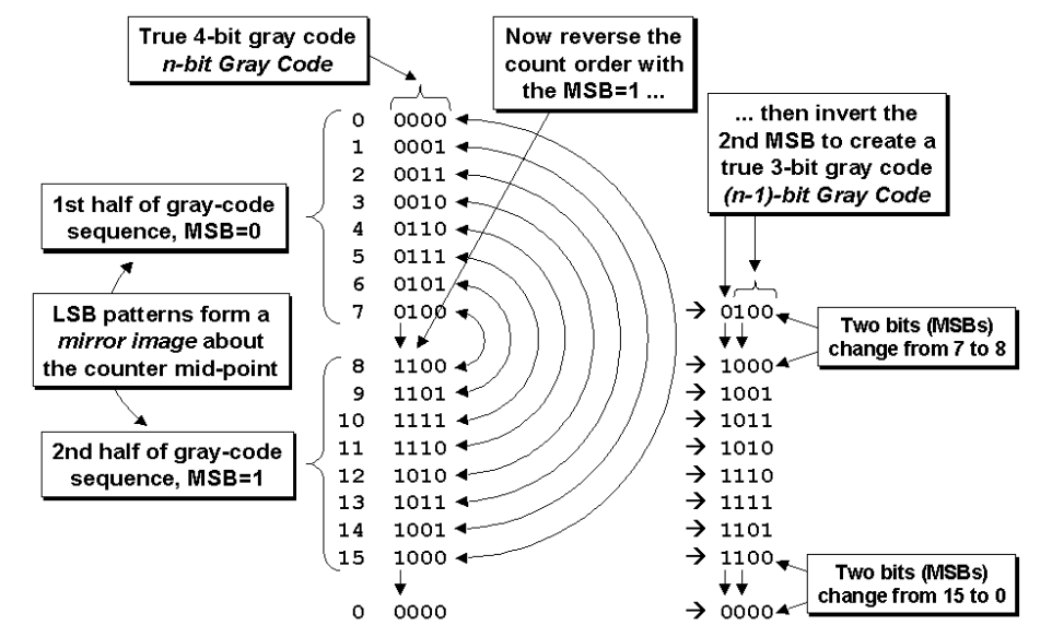
图2. n 位Gary码转换为 (n-1) 位Gary码
To better understand the problem of converting an n-bit Gray code to an (n-1)-bit Gray code, consider the example of creating a dual 4-bit and 3-bit Gray code counter as shown in Figure 2.
为了更好地理解将 n 位 Gray 码转换为 (n-1) 位 Gray 码的问题,请考虑创建一个双 4 位和 3 位 Gray 码计数器的例子,如图2所示。
The most common Gray code, as shown in Figure 2, is a reflected code where the bits in any column except the MSB are symmetrical about the sequence mid-point[6]. This means that the second half of the 4-bit Gray code is a mirror image of the first half with the MSB inverted.
最常见的 Gray 码,如图 2 所示,是一种"反射"代码,其中除 MSB 之外的任何列中的比特都围绕序列中点对称[6]。这意味着 4 比特 Gray 码的后半部分是前半部分的镜像,而MSB 是相反的。
To convert a 4-bit to a 3-bit Gray code, we do not want the LSBs of the second half of the 4-bit sequence to be a mirror image of the LSBs of the first half, instead we want the LSBs of the second half to repeat the 4-bit LSB-sequence of the first half.
若想将 4 位Gary码转换为 3 位Gary码,我们不希望 4 位序列后半部分的 LSB 成为前半部分 LSB 的镜像,而是希望后半部分的 LSB 重复前半部分的 4 位 LSB 序列。
Upon closer examination, it is obvious that inverting the second MSB of the second half of the 4-bit Gray code will produce the desired 3-bit Gray code sequence in the three LSBs of the 4-bit sequence. The only other problem is that the 3-bit Gray code with extra MSB is no longer a true Gray code because when the sequence changes from 7 (Gray 0100) to 8 (~Gray 1000) and again from 15 (~Gray 1100) to 0 (Gray 0000), two bits are changing instead of just one bit. A true Gray code only changes one bit between counts.
仔细观察可以发现,4 位 Gray 码后半部分的第二个 MSB 反转将在 4 位序列的三个 LSB 中产生所需的 3 位 Gray 码序列。唯一的另一个问题是,带有额外 MSB 的 3 位 Gray 码不再是真正的 Gray 码,因为当序列从 7 (Gray 0100) 变为 8 (~Gray 1000), 再从 15 (~Gray 1100) 变为 0 (Gray 0000) 时,变化的是两位而不是一位。真正的 Gray 码在计数之间只变化一位。
3.2 Gray 码计数器基础(Gray code counter basics)
The first fact to remember about a Gray code is that the code distance between any two adjacent words is just 1 (only one bit can change from one Gray count to the next). The second fact to remember about a Gray code counter is that most useful Gray code counters must have power-of-2 counts in the sequence. It is possible to make a Gray code counter that counts an even number of sequences but conversions to and from these sequences are generally not as simple to do as the standard Gray code. Also note that there are no odd-count-length Gray code sequences so one cannot make a 23-deep Gray code. This means that the technique described in this paper is used to make a FIFO that is 2n deep.
关于 Gray 码需要记住的第一个事实是,任何两个相邻字之间的代码距离只有 1 (从一个 Gray 计数到下一个只能改变一位)。关于 Gray 码计数器需要记住的第二个事实是,大多数有用的 Gray 码计数器在序列中必须具有 2 的幂次方的计数。可以创建一个计数偶数个序列的 Gray 码计数器,但在这些序列之间进行转换通常不像标准 Gray 码那样简单。还要注意,没有奇数计数长度的 Gray 码序列,因此无法创建 23 比特深的 Gray 码。这意味着本文中描述的技术被用来创建深度为2n 的FIFO。
Figure 3 is a block diagram for a style #1 dual n-bit Gray code counter. The style #1 Gray code counter assumes that the outputs of the register bits are the Gray code value itself (ptr, either wptr or rptr). The Gray code outputs are then passed to a Gray-to-binary converter (bin), which is passed to a conditional binary-value incrementer to generate the next-binary-count-value (bnext), which is passed to a binary-to-Gray converter that generates the next-Gray-count-value (gnext), which is passed to the register inputs. The top half of the Figure 3 block diagram shows the described logic flow while the bottom half shows logic related to the second Gray code counter as described in the next section.
图 3 是样式 #1 的双 n 位 Gray 码计数器的示意图。该 Gray 码计数器假设寄存器位的输出是 Gray 码值本身 (ptr、wptr 或 rptr)。然后,Gray 码输出被传递给 “Gray 码到二进制码转换器” (bin), 该转换器被传递给一个有条件的二进制值自增器以生成下一个二进制计数值 (bnext), 该值又被传递给“二进制码到 Gray码转换器”,该转换器生成下一个 Gray 计数值 (gnext)并传递给寄存器输入。图 3 的上半部分显示了所描述的逻辑流程,而下半部分显示了下一节将描述的与第二个 Gray 码计数器相关的逻辑。

图 3 双 n-bit Gray 代码计数器
3.3 双 n-bit Gray 码计数器(Dual n-bit Gray code counter)
A dual n-bit Gray code counter is a Gray code counter that generates both an n-bit Gray code sequence (described in section 3.2) and an (n-1)-bit Gray code sequence.The (n- 1)-bit Gray code is simply generated by doing an exclusive-or operation on the two MSBs of the n-bit Gray code to generate the MSB for the (n-1)-bit Gray code. This is combined with the (n-2) LSBs of the n-bit Gray code counter to form the (n-1)-bit Gray code counter[5].
双 n 位 Gray 代码计数器是一种 Gray 代码计数器,它既生成 n 位 Gray 代码序列 (见 3.2 节) 又生成 (n-1) 位 Gray 代码序列。(n-1) 位 Gray 代码是通过对 n-1 位 Gray 代码的两个 MSB 进行排斥或操作来生成的,以生成 (n-1) 位 Gray 代码的 MSB。这与 n-1 位 Gray 代码计数器的 (n-2) LSB 组合在一起,形成 (n-1) 位 Gray 代码计数器 [5]。
3.4 其他Gary码计数器注意事项(Additional Gray code counter considerations)
The binary-value incrementer is conditioned with either an “if not full” or “if not empty” test as shown in Figure 3, to insure that the appropriate FIFO pointer will not increment during FIFO-full or FIFO-empty conditions that could lead to overflow or underflow of the FIFO buffer.If the logic block that sends data to the FIFO reliably stops sending data when a FIFO full condition is asserted, the FIFO design might be streamlined by removing the full-testing logic from the FIFO write pointer.The FIFO pointer itself does not protect the FIFO buffer from being overwritten, but additional conditioning logic could be added to the FIFO memory buffer to insure that a write_enable signal could not be activated during a FIFO full condition.An additional “sticky” status bit, either ovf (overflow) or unf (underflow), could be added to the pointer design to indicate that an additional FIFO write operation occurred during full or an additional FIFO read operation occurred during empty to indicate error conditions that could only be cleared during reset.A safe, general purpose FIFO design will include the above safeguards at the expense of a slightly larger and perhaps slower implementation. This is a good idea since a future co- worker might try to copy and reuse the code in another design without understanding all of the important details that were considered for the current design.
二进制计数器被条件化为 “如果不满” 或 “如果不空” 测试,如图 3 所示,以确保相应的 FIFO 指针在 FIFO 满或 FIFO 空条件下不会增加(这些条件可能导致 FIFO 缓冲区溢出或下溢)。如果向 FIFO 发送数据的逻辑块在断言 FIFO 完整条件时可靠地停止发送数据,则可以通过从 FIFO write指针中删除完整测试逻辑来简化 FIFO 设计。FIFO 指针本身不能保护 FIFO 缓冲区免受覆盖,但可以向 FIFO 内存缓冲区添加额外的条件化逻辑,以确保在 FIFO 完整条件下无法激活 write_enable 信号。可以在指针设计中添加一个额外的 “sticky” 状态位( ovf (溢出) 或 unf (下溢)),指示在满期间发生了额外的 FIFO 写操作、或在空期间发生了额外的 FIFO 读操作这些只能在reset期间清除的错误条件。一个安全、通用的 FIFO 设计将包含上述保障措施,但代价是一个稍大且可能更慢的实现。这是一个好主意,因为未来的复用者可能会试图在另一个设计中复制和重用代码,而不了解当前设计中考虑的所有重要细节。
>>>>>>>>>>>>>>>>>>>持续更新中 Last Modify:25.10.20>>>>>>>>>>>>>>>>>>>>>
参考文献:
《Simulation and Synthesis Techniques for Asynchronous FIFO Design》-- Clifford E. Cummings
[1] Clifford E. Cummings, “Synthesis and Scripting Techniques for Designing Multi-Asynchronous Clock Designs,” SNUG
2001 (Synopsys Users Group Conference, San Jose, CA, 2001) User Papers, March 2001, Section MC1, 3rd paper. Also
available at www.sunburst-design.com/papers
[2] Clifford E. Cummings and Don Mills, “Synchronous Resets? Asynchronous Resets? I am so confused! How will I ever
know which to use?,” SNUG 2002 (Synopsys Users Group Conference, San Jose, CA, 2002) User Papers, March 2002,
Section TB2, 1st paper. Also available at www.sunburst-design.com/papers
[3] Clifford E. Cummings and Peter Alfke, “Simulation and Synthesis Techniques for Asynchronous FIFO Design with
Asynchronous Pointer Comparisons,” SNUG 2002 (Synopsys Users Group Conference, San Jose, CA, 2002) User Papers,
March 2002, Section TB2, 3rd paper. Also available at www.sunburst-design.com/papers
[4] Dinesh Tyagi, former CAE Manager for Synopsys DesignWare product, personal communication
[5] Edward Paluch, personal communication
[6] Frank Gray, "Pulse Code Communication." United States Patent Number 2,632,058. March 17, 1953.
[7] John O’Malley, Introduction to the Digital Computer, Holt, Rinehart and Winston, Inc., 1972, pg. 190.
[8] Steve Golson, personal communication
[9] Synopsys SolvNet, Doc Name: DesignWare-110.html, “Functional Bugs in DesignWare Components,” Updated:
11/30/2000

 浙公网安备 33010602011771号