LogicBlocks & Digital Logic Introduction
LogicBlocks & Digital Logic Introduction
https://learn.sparkfun.com/tutorials/logicblocks--digital-logic-introduction
Introduction
Get up close and personal with the driving force behind the world of digital electronics - digital logic! The LogicBlocks kit is your ticket to discovering digital logic, visualizing how it works, and exploring what it can create.
This tutorial is a continuation of the LogicBlocks Kit Information booklet, which is included with the kit, but we'll regurgitate some of the information in that booklet here. If you've already familiarized yourself with the LogicBlocks kit, I'd encourage you to skip parts 1-3, and head straight down to the experiments in part 4.
Covered In This Tutorial
This tutorial aims to familiarize you with both digital logic and the LogicBlocks. It's split into the following sections:
- What is Digital Logic?
- LogicBlocks Fundamentals
- The Blocks In-Depth
A second tutorial, the Logic Blocks Experiment Guide, follows this tutorial and houses all of the experiments we've concocted with LogicBlocks.
Suggested Reading
Before delving into the LogicBlocks, we recommend reading through these tutorials first:
- Analog vs. Digital -- This tutorial explores the difference between analog and digital signals. Important, since we'll be doing a lot of talking about digital logic.
- Digital Logic -- If you want to go more in-depth into digital logic theory, check out this tutorial.
- Binary -- Binary is the language of computers. Digital logic is a tool we can use to add and store binary numbers.
What is Digital Logic?
!!!
What is Digital?
Electronic signals can be divided into two categories: analog and digital. Analog signals can take any shape and represent an infinite number of possible values. Digital signals have a very defined, discrete set of possible values -- usually only two.
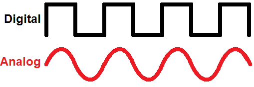
Many electronic systems will use a combination of analog and digital circuits, but at the heart of most computers and other every day electronics are discrete, digital circuits.
What is Digital Logic?
We humans are (mostly) logical beings. When we make decisions and act upon them, logic is working in the background. Logic is the process of evaluating one or more inputs, weighing them against any number of outcomes, and deciding a path to follow. Just like we apply logic to make all of our decisions, computers use digital logic circuits to make theirs. They use a set of standard logic gates to help propogate a decision.
For an in-depth look at digital logic, check out our Digital Logic tutorial!
Where Do We See Digital Logic?
There is logic in all circuits. A connection to a power source is an example of an AND. Only if both power AND ground are connected will the circuit allow electricity to run through it.
Where else? Everywhere! The traffic light in a city uses logic when pedestrians push the walk button. The button starts a process that uses an AND logic gate. If someone pressed the walk button AND there is a red light for traffic where the pedestrian will be walking, the walk signal will activate. If both conditions of this AND statement are not true, the walk signal will never be illuminated.
Inputs and Outputs
A digital logic circuit uses digital inputs to make logical decisions and produce digital outputs. Every logic circuit requires at least one input, before it can produce any kind of output.
Digital logic inputs and outputs are usually binary. In other words they can only be one of two possible values.
There are a number of ways to represent binary values: 1/0 is the least verbose and most common way. However, you may also see them in a boolean representation like TRUE/FALSE or HIGH/LOW. When the values are represented at a hardware level, they might be given actual voltage levels: 0V [Volts] is a 0, while a higher voltage - usually 3V or 5V - is used to represent a 1.
| 1 | 0 |
| HIGH | LOW |
| True | False |
| 5V (Volts) | 0V |
Logic Gates
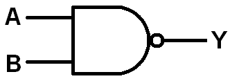
To make their logical decisions, a computer will use any combination of three fundamental logic functions: AND, OR, and NOT.
- AND -- The AND function produces a TRUE output if and only if all of its inputs are also TRUE.
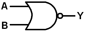
- OR -- An OR will prove TRUE if any (one or more) of its inputs are also TRUE.
- NOT -- The NOT operator has only one input. The NOT operator negates its input, which means the output will be the opposite of the input.
Each of those functions can be realized using logic gates. Logic gates are what we use to create digital logic circuits. They're the building blocks of computers and other electronics . They take one or more inputs, perform a specific function (AND, OR , NOT, etc.) on them, and then produce an output based on that function.
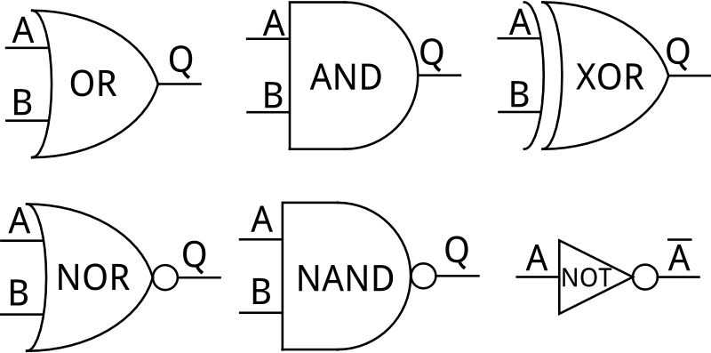
Logic gates all have specific circuit symbols, just like resistors, capacitors, and inductors. And, just like standard electronic component symbols, logic gates can be diagrammed in a schematic by connecting their input and output lines together.
Truth Tables
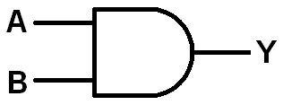
The 'logic' of a logic gate or function can be represented in a number of ways including truth tables, venn diagrams and boolean algebra. Among those, truth tables are the most common. Truth tables are a complete listing of every possible input combination, and the output they produce.
All inputs are arranged on the left side of the table, while the output is on the right. Every row of the table represents one possible input combination.
| Input A | Input B | Output Y |
|---|---|---|
| 0 | 0 | 0 |
| 0 | 1 | 0 |
| 1 | 0 | 0 |
| 1 | 1 | 1 |
Above is the truth table of an AND gate. An AND gate has two inputs and one output, so the truth table has two columns for input and one column for output. Two input values means there are four possible input combinations: 0/0, 0/1, 1/0, and 1/1. So, the AND gate's truth table will have four rows, one for each combination of inputs. The only case where the output of AND is 1 is when both inputs are also 1.
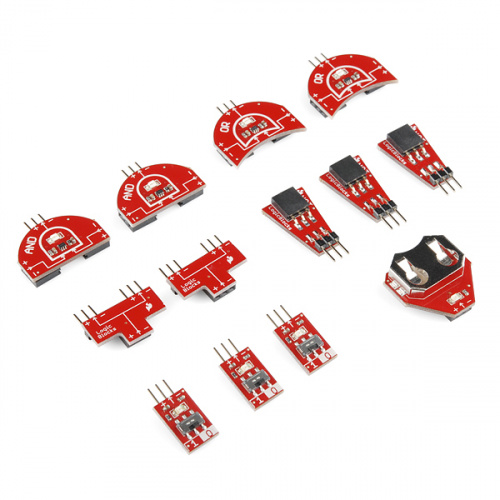
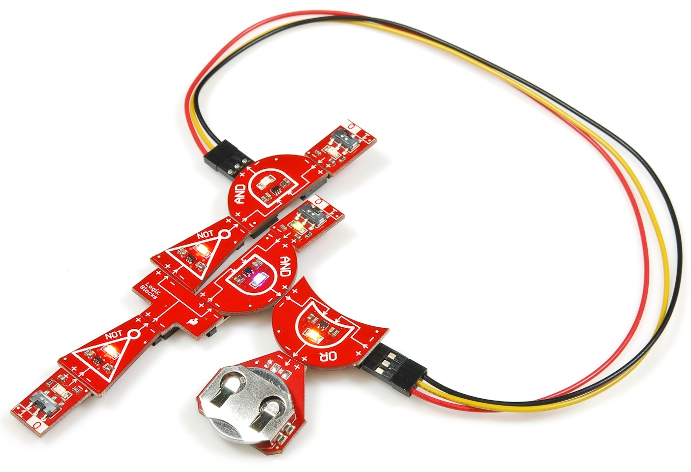
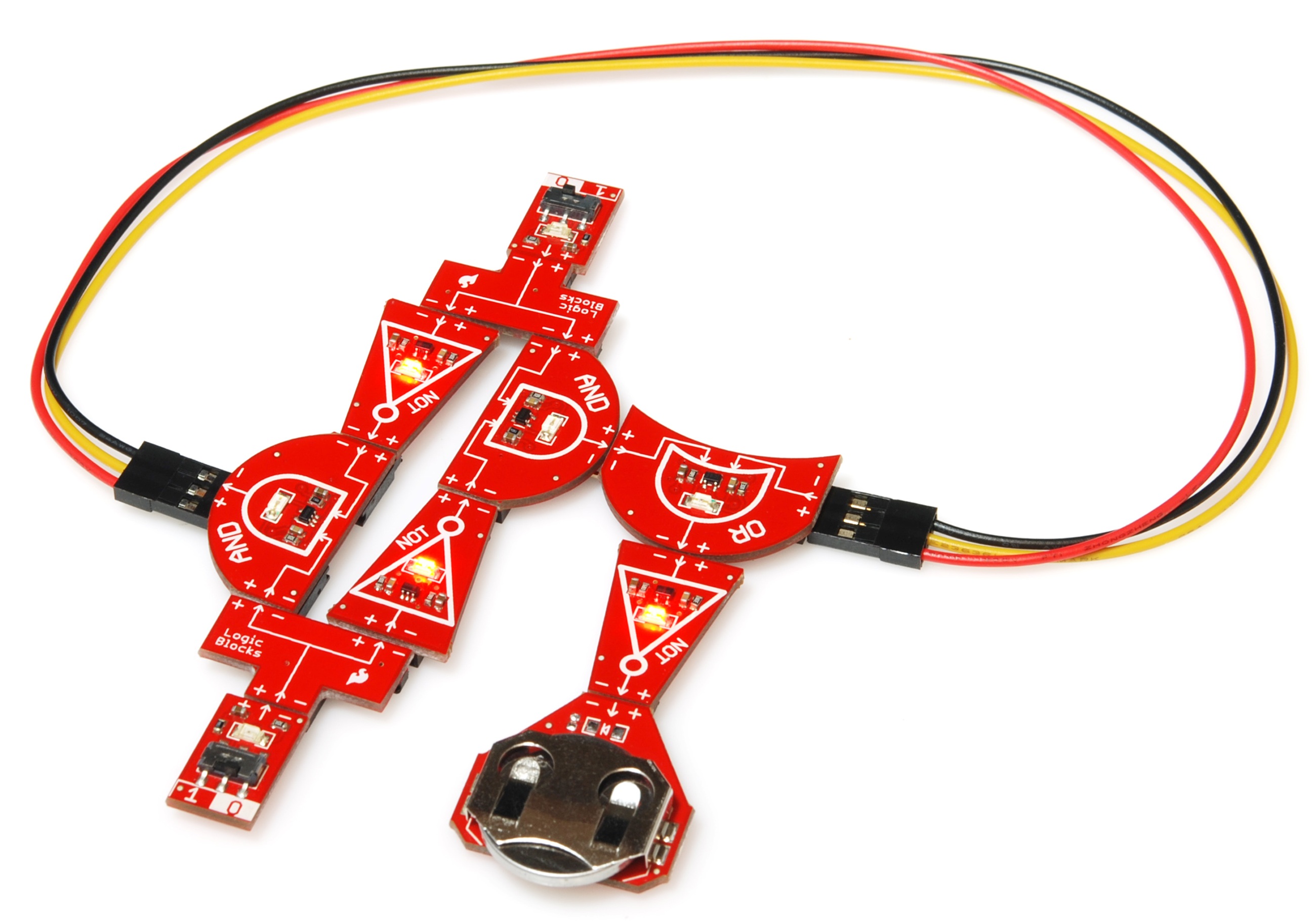
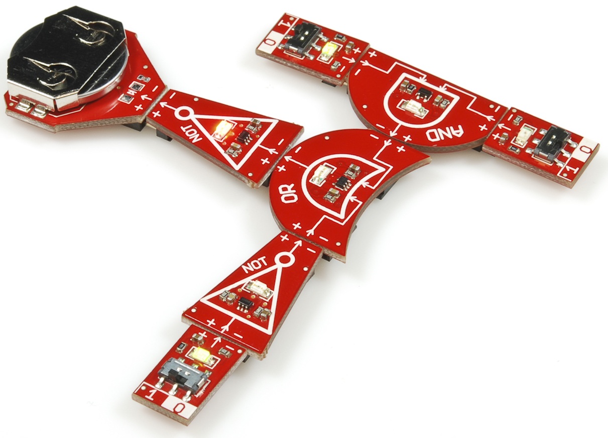
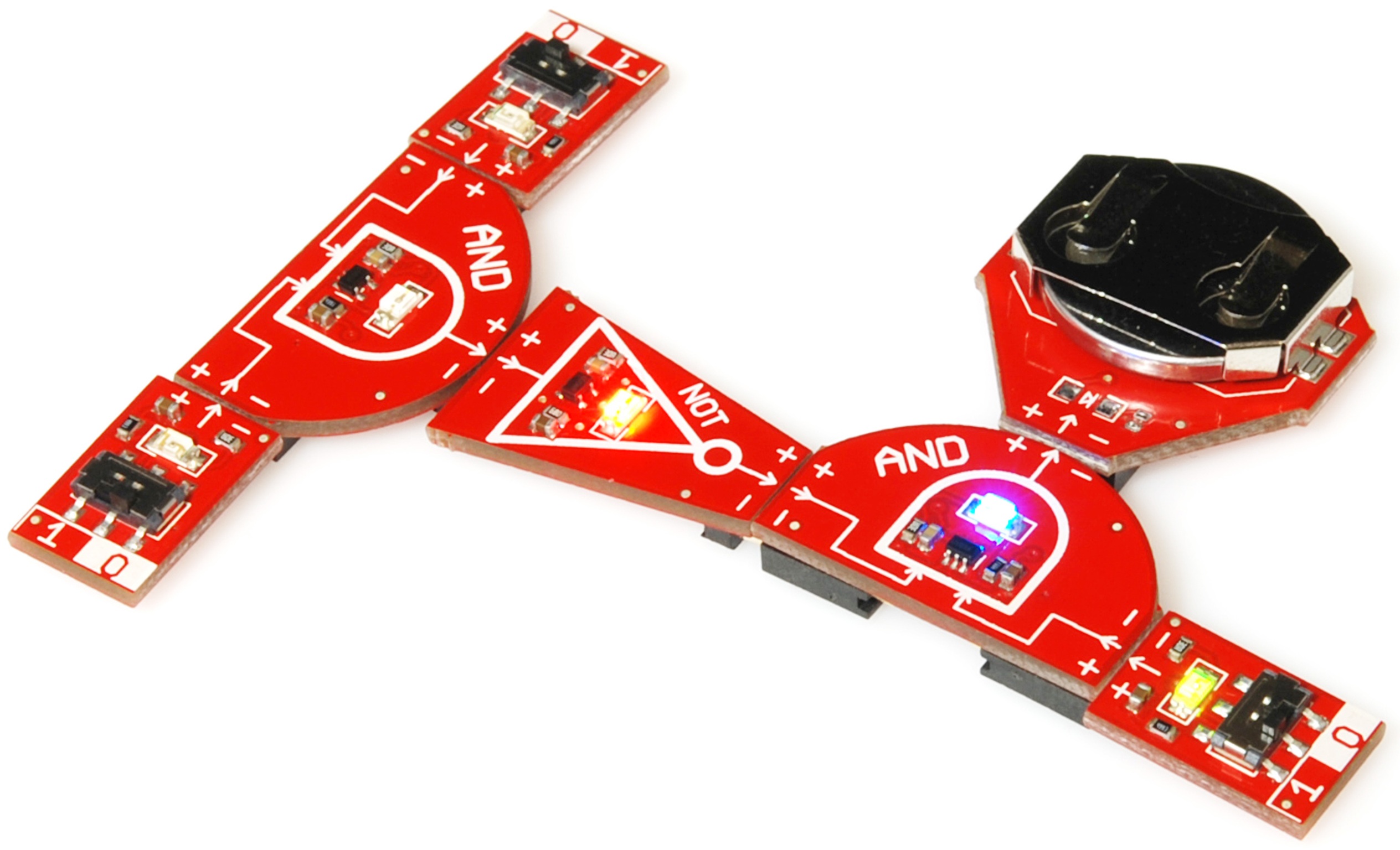
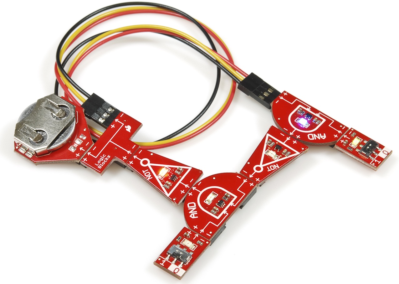
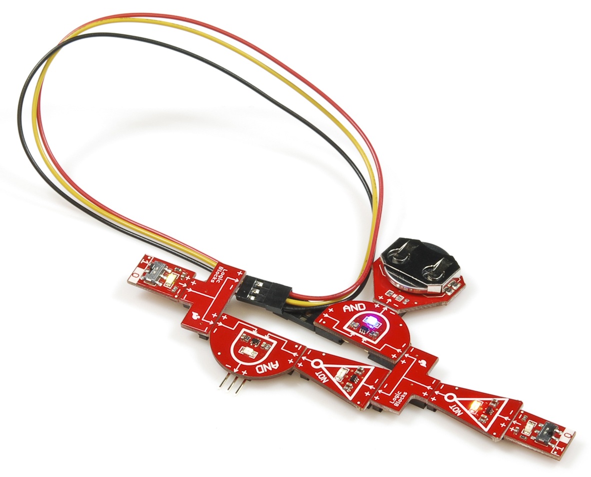
LogicBlocks Fundamentals
There are six separate LogicBlocks, which can be divided into three categores: logic gates, input blocks and utility blocks.
Logic Gate Blocks
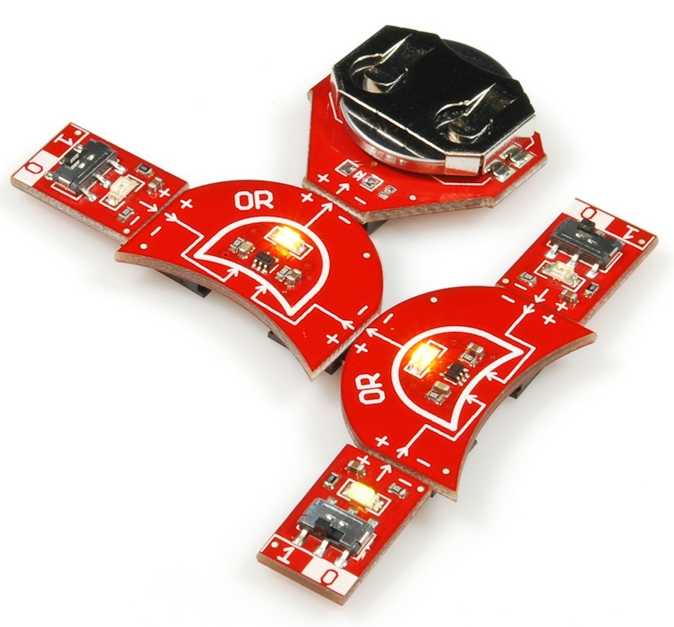
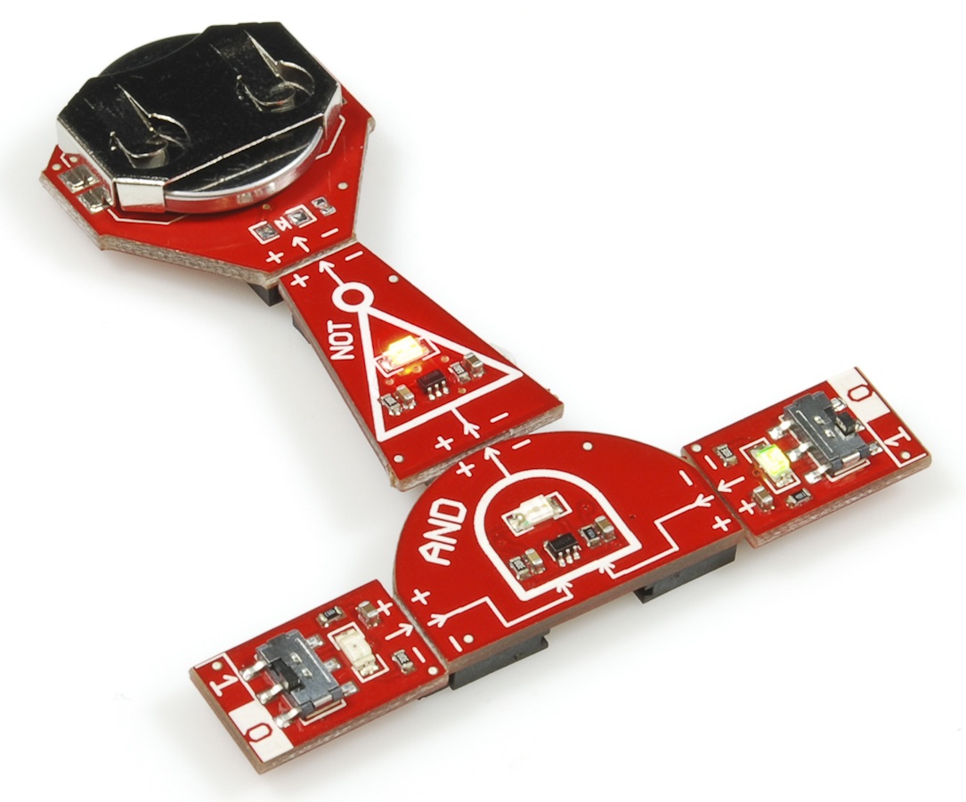
There are three different logic gate LogicBlocks: AND, OR, and NOT - the fundamental logic gates. They're shaped (as much as possible) like their circuit diagram equivalents, and also labeled with their gate name.
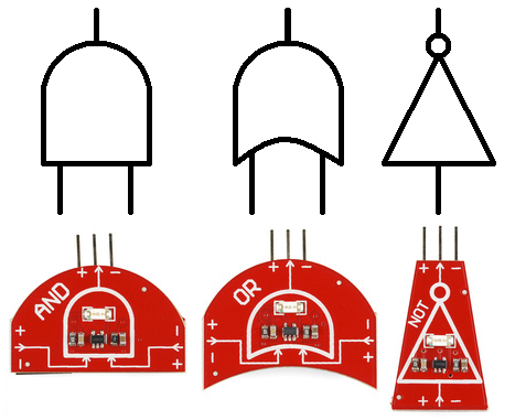
Each gate has one output, a male header (the pointy one). The female headers represent the inputs; the AND and OR gates have two inputs, while the NOT gate has just one.
The logic gate LogicBlocks each have an LED, which represents their output status. An illuminated LED represents a logic gate producing a 1, while an unlit LED means the gate is producing a 0.
Input Blocks
The input blocks are what you'll use to supply LogicBlocks with digital inputs. They have a switch to set the output of the Input block to either 0 or 1. The LED on the Input block displays what value the block is sending out.
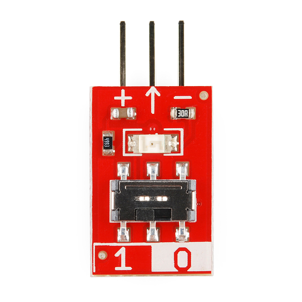
The input blocks have a single, male, output header. This should be plugged into the female inputs of the gate LogicBlocks.
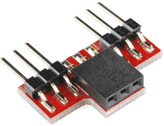
Utility Blocks (and Cables)
Key among the utility boards is the Power block. Each Logic gate requires power to operate, and this board is there to supply it. The Power block has a single, female, input header, and should be plugged into the output of the last logic gate. You'll only need ONE power block to supply power to an entire digital logic circuit.
There's also a Splitter LogicBlock, which simply divides one input into two outputs. It doesn't perform any operation on the signal, just passes it through. This'll come in handy when you create more complicated digital logic circuits which require one input to run into two or more logic gates.
Also lumped into this category is the feedback cable. This cable will usually be used in conjunction with the splitter block, for more advanced LogicBlock circuits.
The Rules
There's really only one rule when it comes to playing with LogicBlocks: When connecting an output of one block to the input of another, make sure each of the three pins match up. Each of the inputs and outputs consist of three pins: Power (“+”), Ground (“−”), and Signal (“->”).
You'll also need to make sure there's always one (and only one) Power Block connected to your LogicBlock circuit.
All inputs of a logic block (or cable) should have the output of another block (or cable) attached to them. If an input is left floating (not connected), the gate won't know if the input is a 1 or a 0, and, as a result, the output will be unreliable.
Response Times
Logic gates form their output decisions faster than any human could ever detect (we're talking nanoseconds). So to make the process more visible, we've slowed the LogicBlocks down so you can see the process they go through. If you've got a long line of logic blocks, this delay will allow you to more visually see how the outcome of one block affects the input of another.
The delay is on the order of half a second. Just long enough to see what's going on.
The Blocks In-Depth
On this page we'll dig into the gritty details of each component in the LogicBlocks kit. We'll talk about what each block's purpose is, examine their truth tables, and look at what other blocks they can plug into.
Here are some quick-links to the blocks we'll be covering on this page:
- Input LogicBlock
- AND Gate LogicBlock
- OR Gate LogicBlock
- NOT Gate LogicBlock
- Power LogicBlock
- Splitter LogicBlock & Feedback Cable
Input LogicBlock
The Input Blocks make the LogicBlocks world go 'round. These small rectangular blocks have one male connector, which plugs into the female input pins of gate blocks, power blocks, and splitters.
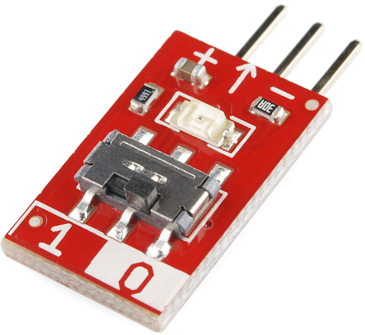
Each Input Block has a two-position switch, which you'll use to set the block as either 1 or 0 (TRUE or FALSE, ON or OFF).
A green LED on the Input Block represents the value it outputs. An illuminated LED indicates that the block is set as 1. If the LED is off, the output value is 0.
AND Gate LogicBlock
The AND LogicBlock is a two-input, single-output AND gate. The block is in a "D shape", much like the AND gate circuit symbol. The two female input headers are located on either side of the AND Block. The output of the AND Block is located at the middle-top.

You can connect either an Input Block or the output from another Gate Block to these inputs. The male output header can be plugged into either the input of another gate or a Power Block.
Each AND Gate Block has a single blue LED, which represents the output of the gate. If the LED is on, then that means the AND Gate is producing a 1 (TRUE, ON) at the output. If the LED is off, then the AND Gate's output is 0.
AND Truth Table, Circuit Symbol, Boolean Notation
Here's a truth table for the AND Block:
| Input A | Input B | Output |
|---|---|---|
| 0 | 0 | 0 |
| 0 | 1 | 0 |
| 1 | 0 | 0 |
| 1 | 1 | 1 |
And the circuit symbol for an AND gate, which you'll get very used to seeing:
The boolean equation symbol for AND is the centered dot (·). For example, the gate above could be represented by the equation: A · B = Y.
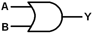
OR Gate LogicBlock
The OR LogicBlock is a two-input, single-output OR gate. The block is shaped like and OR gate circuit symbol -- a convex arc on the output side, and a concave arc on the input side. The two female inputs are located on either side of the OR Block. The output of the OR Block is located at the middle-top of the block.
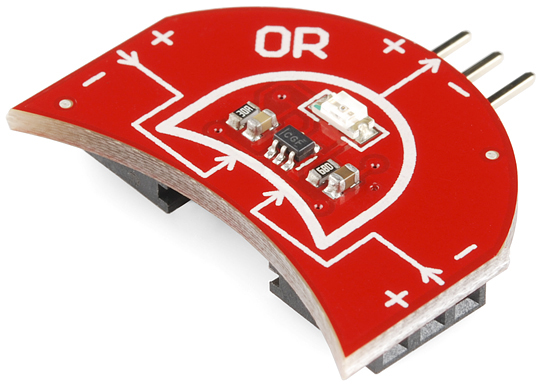
You can connect either an Input Block or the output from another Gate Block to either of the two inputs. This male output connector can be plugged into either the input of another gate, or a Power Block.
Each OR Gate Block has a single yellow LED, which represents the output of the gate. If the LED is on, that means the OR Gate is producing a 1 (TRUE, ON) at the output. If the LED is off, then the OR Gate's output is 0.
OR Truth Table, Circuit Symbol, Boolean Notation
Here's a truth table for the 2-input/1-output OR gate:
| Input A | Input B | Output |
|---|---|---|
| 0 | 0 | 0 |
| 0 | 1 | 1 |
| 1 | 0 | 1 |
| 1 | 1 | 1 |
And the circuit symbol, shaped much like the block itself:

We can represent digital logic using boolean equations. The boolean equation symbol for OR is the plus sign (+). Here's the boolean equation for the OR circuit above: A + B = Y.
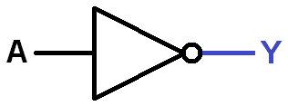
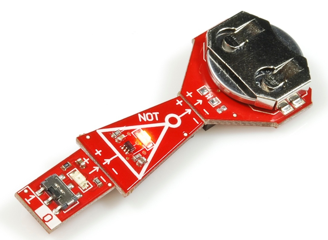
NOT Gate LogicBlock
The NOT LogicBlock is a single-input, single-output NOT Gate. The Block comes in a trapezoid shape (it's as close as we could get to the triangle-shaped NOT gate circuit symbol). The female input connector is located on the side with the larger edge. The output of the NOT Block is located on the smaller edge.
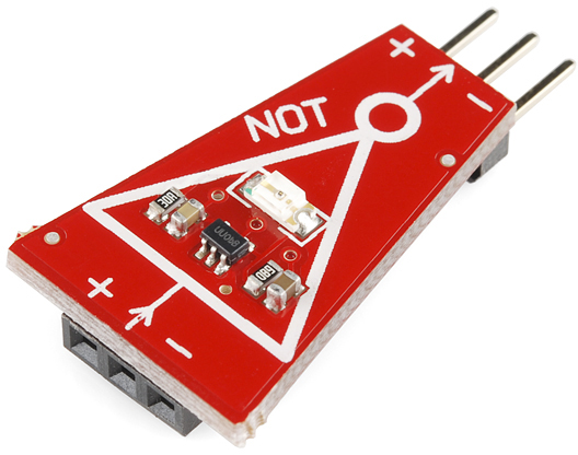
You can connect either an Input Block or the output from another Gate Block to this input. This male connector can be plugged into either the input of another gate or a Power Block.
Each NOT Block has a single red LED, which represents the output of the gate. If the LED is on, then that means the NOT Gate is producing a 1 (TRUE, ON) at the output. IF the LED is off, then the NOT gate's output is 0.
NOT Truth Table, Circuit Symbol, Boolean Notation
A NOT gate is often called an inverter because it inverts any signal it receives. A 0 turns into a 1, and a 1 turns into a 0. An inverter's truth table looks something like this:
| Input A | Output |
|---|---|
| 0 | 1 |
| 1 | 0 |
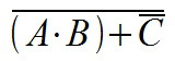
When writing boolean equations, the NOT operation is usually indicated by a bar over any variables it inverts. For example the boolean equation for the circuit above would simply be:  .
.
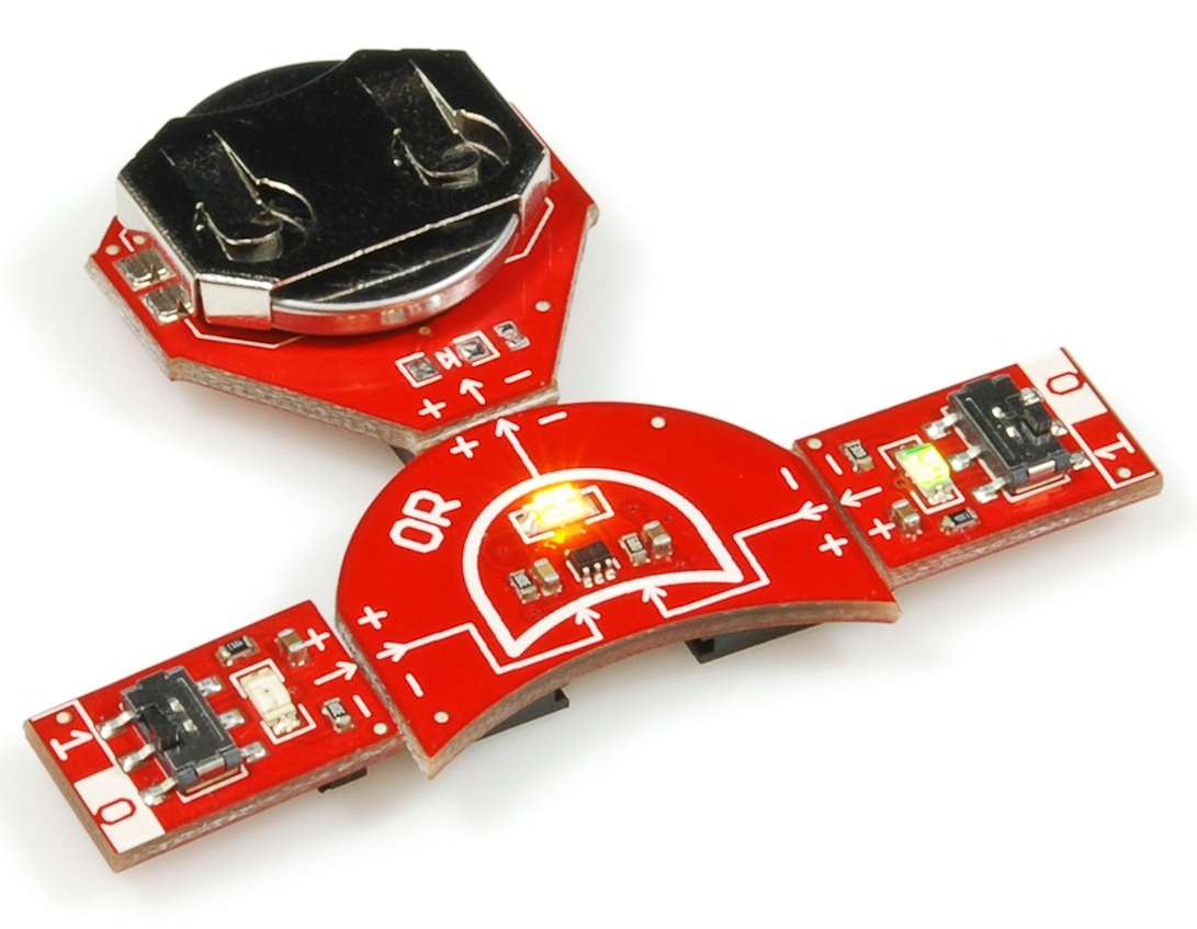
Power LogicBlock
No electronic circuit can work without some form of power. Enter the Power Block!

The Power Block runs on a single 20mm coin cell battery, which optimally provides around 3V, and should last for quite a while. The LogicBlocks can work at voltages between 2 and 5V, and they consume very little current.
The Power Block has a single female connector, which should be connected to the output of a Gate Block. Only one Power Block should be connected in any circuit.
The Power Block is the final piece to any LogicBlock circuit. It should be connected to the output of the very last Logic Block gate.
Splitter LogicBlock and Feedback Cable
The Splitter Block allows the output of one Block to feed into the inputs of two separate Blocks.
For more advanced circuits you'll want to spread inputs to multiple gates, or add feedback. This is where both the Splitter Block and Feedback Cable come in handy. Often the Feedback Cable will be connected to one of the two Splitter Block outputs.
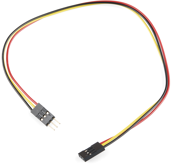
The Feedback Cable is made of three separate wires -- colored red, yellow, and black. Red should always be connected to the + pin, black to the − pin, yellow will pass the signal through.
LogicBlocks Experiments
Now that you've been introduced to the fundamentals of LogicBlocks and digital logic, it's time to experiment! In the LogicBlocks Experimenter's Guide we'll build all sorts of fundamental logic circuits with the handful of components you've been introduced to. Like this 2-to-1 multiplexer:
For all LogicBlocks experiments, please head over to the LogicBlock Experimenter's Guide!
=================
LogicBlocks Experiment Guide
https://learn.sparkfun.com/tutorials/logicblocks-experiment-guide/introduction
Introduction
So you've read through the LogicBlocks introductory tutorial (or the kit's included documentation), and are ready for some experiments!? Time to put those LogicBlocks to use!
You'll be building big ol' LogicBlock circuits like this XNOR in no time!
Table of Contents
Here's a breakdown of the experiments we'll be exploring in this guide:
- 2-Input AND Gate
- 3-Input AND Gate
- NANDs, NORs, and De Morgan's Laws
- Combinational Logic
- Ring Oscillator
- SR Latch
- 2-to-1 Multiplexer
- 1-to-2 Decoder (De-multiplexer)
- XOR Gate
- Beyond LogicBlocks...
Each experiment includes a schematics, and matching LogicBlock layouts for the circuit under test.
There are also smatterings of truth tables, state diagrams, and boolean equations throughout each experiment. And they're all capped off with challenges, questions, and sub-experiments. To get the most out of each experiment, make sure you check out the sub-experiments!
1. 2-Input AND Gate
The first experiment starts off as simple as possible: a dual-input, single output AND gate.
What You'll Need
- 1x AND Block
- 2x Input Blocks
- 1x Power Block
Circuit Diagram

LogicBlock Layout
Nothing too fancy here. An Input Block should be inserted into each of the AND Block's inputs. Then plug the Power Block into the output of the AND Block.

The blue LED on the AND Block will indicate the output status of the circuit.
The Experiment
Try all four possible input combinations: 0/0, 0/1, 1/0, and 1/1. Remember, this is what the AND gate's truth table should look like:
| Input A | Input B | Output |
|---|---|---|
| 0 | 0 | 0 |
| 0 | 1 | 0 |
| 1 | 0 | 0 |
| 1 | 1 | 1 |
- Does the blue AND block LED light up as you'd expect?
Sub-Experiments
While we're here, let's discuss the other two fundamental gates. A two-input OR and a single-input NOT.
Two-Input OR Gate
Can you lay out the fundamental, two-input OR gate with LogicBlocks? It'll require a similar set of blocks to the AND:
After experimenting with that, can you complete this truth table for the OR?:
| Input A | Input B | Output |
|---|---|---|
| 0 | 0 | |
| 0 | 1 | |
| 1 | 0 | |
| 1 | 1 |
Two-Input NOT Gate
Now do the same thing with the NOT gate.
This time you'll only need one Input Block:
Can you complete the NOT truth table?
| Input A | Output |
|---|---|
| 0 | 1 |
| 1 | 0 |
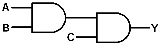
2. 3-Input AND Gate
Sometimes you need to AND more than two inputs together. In fact, 3- and 4-input AND gates are just as common as the dual-input variety. Let’s make a 3-input AND gate out of two two-input AND gates.
What You'll Need
- 3x Input Blocks
- 2x AND Blocks
- 1x Power Block
Circuit diagram
LogicBlock layout
Start by building the 2-input AND block from the last experiment, but plug the output of that into the input of another AND. Then add an Input Block to the second AND's second input.
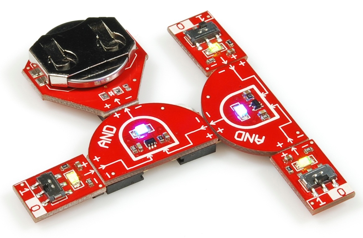
Complete the circuit by adding a Power Block to the output of the second AND.
The blue LED on the second AND gate represents the output of this circuit.
The Experiment
With three total inputs, how many different input combinations can you make? 8! This number grows exponentially at 2n, where n is the number of inputs. So, a 4-input AND gate has 16 possible combinations, 5 inputs would be 32 outputs, and so on.
Try all possible input combinations and fill out the truth table below:
| Input A | Input B | Input C | Output Y |
|---|---|---|---|
| 0 | 0 | 0 | |
| 0 | 0 | 1 | |
| 0 | 1 | 0 | |
| 0 | 1 | 1 | |
| 1 | 0 | 0 | |
| 1 | 0 | 1 | |
| 1 | 1 | 0 | |
| 1 | 1 | 1 |
- Can you think of a situation in real life where three requirements must be met before an outcome becomes true?
- If you had more AND blocks, can you imagine what a 4-input AND block might look like?
Sub-Experiments
Try using two OR gates and three Input Blocks to create a 3-input OR gate.
- Draw a schematic diagram for this circuit.
- Write out a truth table for this circuit. Like the 3-input AND circuit, this circuit will have 8 possible sets of input. But there should be a lot more 1's on the output column!
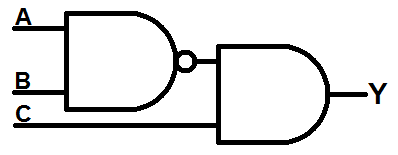
3. NANDs, NORs, and DeMorgan's Laws
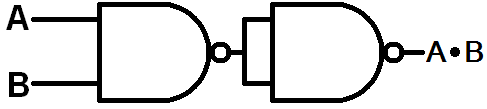
NAND -- in other words NOT AND or negated AND -- is what you get when you place an inverter at the output of an AND gate. NAND gates are very popular in the world of digital logic. They’ve even got their very own circuit symbol, an AND gate with a “bubble” at the output:
Let's make one with LogicBlocks!
What You'll Need
- 1x AND Block
- 1x NOT Block
- 2x Input Blocks
- 1x Power Block
LogicBlocks Layout
This layout is similar to the setup from experiment 1, with the addition of a NOT gate between the AND Block output and the Power Block.
The output of this circuit is represented by the red LED on the NOT gate.
The Experiment
Two inputs means four possible input combinations. Try them all and fill out the 2-input NAND gate's truth table:
| Input A | Input B | Output |
|---|---|---|
| 0 | 0 | 0 |
| 0 | 1 | 0 |
| 1 | 0 | 0 |
| 1 | 1 | 1 |
- How does that compare to the truth table of the AND gate?
Sub-Experiments
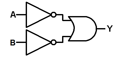
You can also negate an OR gate to create a NOR:

Which also has its own "bubbled" circuit symbol:
- What does the 2-input NOR gate's truth table look like?
DeMorgan's Law
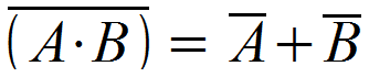
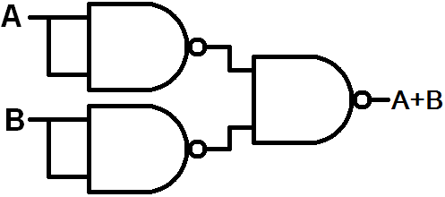
All of this NAND and NOR discussion has me itching to discuss De Morgan's Law! De Morgan's Law allows us to convert NANDs to OR, and NORs to ANDs. There are two parts to De Morgan's Law:
- A 2-input NAND is equivalent to OR-ing two inverted inputs. In boolean equation terms:
![]()
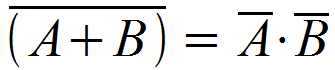
- A 2-input NOR is equal to AND-ing two inverted inputs. Or, in boolean terms:
![]()
Prove it yourself! Build the circuit below with your LogicBlocks, and compare the truth table you filled out for the NAND gate with the truth table for this circuit -- two inverted inputs running into an OR gate.
Are the truth tables the same? You've just verified the first part of DeMorgan's law!
Now, you might be asking: "what's the point?" Well, a big part of digital logic is simplifying the circuit, and using a few gates as possible. Thanks to De Morgan's Law, we can use a NAND gate to stand in for all of the other gates.
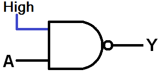
For example, a NOT can be made out of a NAND by simply tying one the inputs permanently high:
Or use three NAND gates to make an OR:
Or use two NANDs to make an AND:
The versatility of NAND gates makes them truly magical!
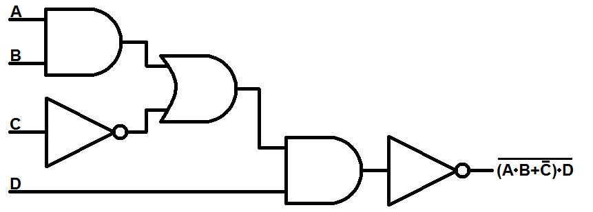
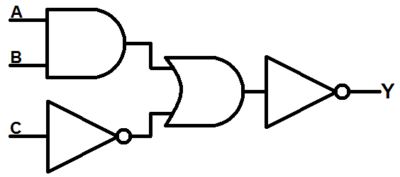
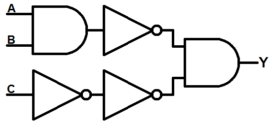
4. Combinational Logic
The circuits in the previous experiments have all been examples of combinational logic circuits. In combinational circuits the output depends exclusively on the current state of the inputs. The circuit flows in one direction, from the inputs (traditionally) on the left, to the outputs on the right.
The opposite of combinational logic is sequential, in which a circuit's current output will affect its future outputs. But we'll get to that in later experiments.
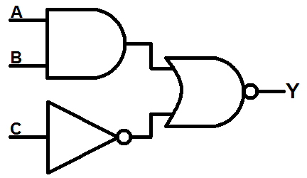
Here's an example of a combinational logic circuit we can build with LogicBlocks:
Given the input names shown in the circuit diagram (A and B feeding into the AND gate, C goes through the first NOT gate), we can form a boolean equation like this:
The output is the negation of ((A and B) or not C) (not the order of operations!). Let's build the above circuit with LogicBlocks!
What You'll Need
- 1x AND Block
- 1x OR Block
- 2x NOT Blocks
- 3x Input Blocks
- 1x Power Block
LogicBlock Layout
The output of an AND Block with two Input Blocks should be connected to one input of an OR Block. The other input of the OR Block should be connected to a NOT Block, which has an Input Block feeding into it. Finally, the output of the OR Block should feed into another NOT block, which is connected to a Power Block.
The output of this combinational logic circuit is represented by the red LED on the final NOT Block.
The Experiment
Try all eight possible input combinations and fill out this circuit's truth table:
| Input A | Input B | Input C | Output Y |
|---|---|---|---|
| 0 | 0 | 0 | |
| 0 | 0 | 1 | |
| 0 | 1 | 0 | |
| 0 | 1 | 1 | |
| 1 | 0 | 0 | |
| 1 | 0 | 1 | |
| 1 | 1 | 0 | |
| 1 | 1 | 1 |
- Does that jive with the equation from above?
- Have another look at that equation, or even the schematic. Recognizing the NANDs and NORs, could the equation be simplified by using De Morgan's Laws? Yes! First, push that inverter into the OR gate to turn it into a NOR:
Then apply De Morgan's law: push the bubble through the NOR gate - turning that gate into an AND - and through to create NOT gates on both inputs:
The two NOT gates on the C input would cancel each other out, so just get rid of them both. The NOT gate on the first AND's output can be pushed onto the gate to create a NAND gate:
We've completely eliminated the OR gate! Would you believe that this circuit produces the same truth table as the circuit at the beginning of this experiment? Try it out for yourself:
Sub-Experiments
- The next experiment takes a pretty giant leap from combinational to sequential logic. At this point, we'd really encourage you to just play around with the LogicBlocks, create your own circuits. Then try to draw out a circuit diagram, and a truth table.
- Are there any real-life scenarios you could imagine solving with digital logic?
5. Ring Oscillator
An oscillator is a circuit whose output periodically and repetitively fluctuates. Oscillators are a critical part of most electronic circuits; they're used to create anything from a clock to radio waves. There are a variety of circuits that can create oscillation, you can use op amps, crystals, 555 timers, and, of course, logic gates!
By stringing an odd number of NOT gates together, and introducing feedback -- looping the output of the last inverter back to the input of the first -- we can create a ring oscillator. Let's LogicBlock it!
What You'll Need
- 3x NOT Blocks
- 1x Splitter Block
- 1x Feedback Cable
- 1x Power Block
Circuit Diagram
This circuit introduces a concept we've only briefly mentioned so far: sequential circuits. Unlike combinational circuits, the output of a sequential circuit depends on previous output states.
Here is the circuit for a ring oscillator:
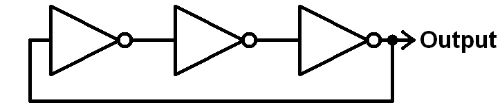
See how the output of third and final NOT gate splits into two directions? The first goes straight out to the output, like we're used to, but it also loops back into the input of the the first NOT gate. This is called feedback -- a term almost synonymous with sequential circuits. The current state of the output depends on what it was doing in the past.
LogicBlock Layout
First link up three NOT gates and plug the third into a Splitter Block. Use the Feedback Cable to connect one of the Splitter Block outputs to the input of the first NOT gate. Finally, plug the Power Block into the second output of the Splitter Block.
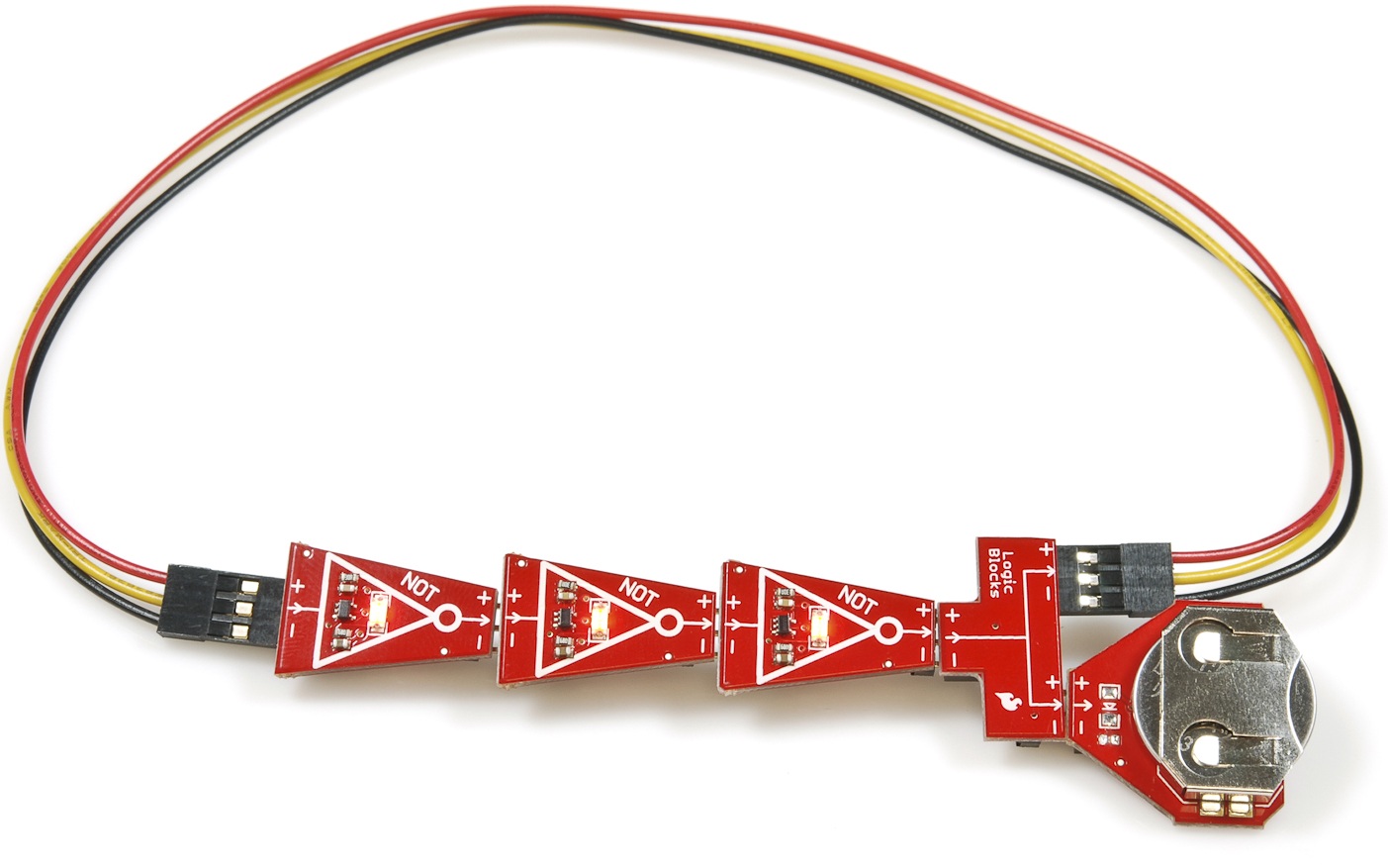
The output of this circuit is represented by the red LED on the third and final NOT block.
The Experiment
What does the truth table look like for this circuit? Wait. Does it even have a truth table? There aren't any inputs! Instead of a standard truth table, we can create a state table that defines the value of the current output as dependent on the previous output:
| Previous Output | Current Output |
|---|---|
| 0 | 1 |
| 1 | 0 |
- Does the number of inverters have to be odd? What happens if there are an even number of inverters? Try removing one of them.
- Can you calculate how fast the LED on the final NOT Block is blinking? Each block has a delay of about 1 second. What effect would increasing the number of inverters to 5 have on the blinking rate of the output?
Sub-Experiments
In some cases it may be handy to have an enable input on your oscillator. Enable inputs -- commonly found in many digital logic circuits -- control the overall operation of the circuit. When the enable input is set to 1, the circuit operates as normal, but when its set to 0 the circuit's operation is halted.
We can add an enable input to the ring oscillator by introducing an AND gate. Have a look at this circuit diagram:
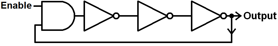
Build it by plugging an AND Block into the first NOT gate (removing the feedback cable). Then plug the male end of the feedback cable into one of the AND Block's inputs, and an Input Block (our enable) into the other input.
Now flip the switch on the enable input to see how it affects the output of the oscillator.
What would the state table look like now?
| Enable | Previous Output | Current Output |
|---|---|---|
| 0 | 0 | |
| 0 | 1 | |
| 1 | 0 | |
| 1 | 1 |
6. SR Latch
A latch (also called a flip-flop) is a fundamental component of data storage. A single latch can hold 1-bit of data, increase that number by many orders of magnitude and you can create kilo-, mega-, giga-, even tera-bytes of memory. Of course, like most digital circuits, latches are made out of digital logic gates!
There are many different kinds of latches, all with somewhat cryptic names like SR, D, JK, and T. The SR-latch we'll be experimenting with is one of the most fundamental forms of a latch.
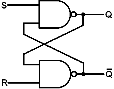
There are a few ways to make an SR latch. Here’s an example of a NOR SR latch:
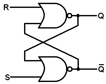
Notice the feedback? This is another sequential logic circuit. The two NOR gates each have their output flow into the input of the other. There are two controllable inputs: reset (R) and set (S), which produce the two outputs: Q and Q' ("Q-not"). That's where the SR latch get's its name -- it's a set/reset latch.
The SR latch comes with a rule, which cannot ever be broken: Q' must always be the opposite of Q. These outputs are called complements. In our application Q is the only output we really care about -- that's where the latch's data is usually stored and retreived -- but it's important to observe that the two outputs are opposites.
An SR latch is so important it even gets its very own circuit symbol:

Here is the state table, which is a bit wonky. Because the circuit is sequential, the current value of Q depends on its previous state:
| S | R | Previous Q | Current Q | Current Q' |
|---|---|---|---|---|
| 0 | 0 | 0 | 0 (no change) | 1 |
| 0 | 0 | 1 | 1 (no change) | 0 |
| 0 | 1 | 0 | 0 (no change) | 1 |
| 0 | 1 | 1 | 0 | 1 |
| 1 | 0 | 0 | 1 | 0 |
| 1 | 0 | 1 | 1 (no change) | 0 |
| 1 | 1 | 0 | 0 (Restricted, Q and Q' would not be complements) | 0 |
| 1 | 1 | 1 | 0 (Restricted, Q and Q' would not be complements) | 0 |
Put into words, the output, Q, can be in any of the following states:
- Steady: When S and R are both 0, then Q remains steady. It keeps the value it had before. If it was 0 it'll remain 0, if it was 1 it will still be 1.
- Set: Changing S to 1 has the potential to "set" the output of Q. If Q was 0, changing S to 1 will change Q to 1 as well. If Q was already 1, making S=1 will have no effect.
- Reset: Moving the R input from 0 to 1 can "reset" Q. As long as Q was 1, setting R to 1 will change Q to 0. If Q was already 0, though, R won't have any effect on it.
- Restricted: When both S and R are 1, we enter restricted territory: our rule that Q and Q' must be complements is broken, as they both go to 0. So we call S=1/R=1 a restricted combination. In most latch circuits precautions are taken to keep those inputs from both being 1. Our LogicBlock circuit isn't quite that smart, so you'll need to take the "circuit safety" precautions into your own hands to make sure they're never both 1 (don't worry, the universe should survive the contradiction if you set both inputs high).
We can also use a state diagram to document the possible states of Q:

Enough conceptual stuff. Let's lay out the SR latch with LogicBlocks!
What You'll Need
- 2x OR Blocks
- 2x NOT Blocks
- 2x Input Blocks
- 1x Splitter Block
- 1x Feedback Cable
- 1x Power Block
LogicBlock Layout
Construct the LogicBlock circuit like below:
In our mind, we need to assign names to both inputs. One should be R (reset) the other should be S (set). Because the circuit is symmetric, it doesn't matter which input we call which, but the name of the input will affect which output is which.
There are two outputs to keep an eye on in this circuit; both are indicated by the red LEDs on the NOT gates. The NOT gate coming out of the OR gate with S as its direct input indicates the Q' output. Our Q output is indicated by the red LED on the NOT gate fed by the OR gate with R as its input.
The Experiment
Give this series of steps a try, and observe both Q and Q' outputs.
- We need an initial state to start us off. Begin by setting both S=0 and R=0.
- Now, set R=1. Q should "reset", if it wasn't already 0, it will become 0. If Q already was 0, it will stay there. Obeying our rule, Q' should be 1.
- Set R=0. Nothing should change on Q or Q'. They hold steady.
- Set S=1. Now Q should 'set' and go high, while Q' goes low.
- Set S=0. There shouldn't be any effect on Q or its complement.
- Can you see how this might work as a piece of memory? Imagine a single bit of data being stored in the Q output!
- Try entering the restricted state by setting both S and R to 1. Q and Q' should both be 0; our complement rule has been broken! To avoid this from happening safeguards will usually be placed on the inputs (in the form of more logic gates!), which will convert the restricted combination to an allowed input value.
Sub-Experiments
You can also make a latch out of NAND gates. Just swap the ORs with ANDs. Too keep the names of the inputs in line with the outcome they produce, we also swap the S and R inputs (or Q and Q', depending on how you look at it).
And lay it out with Logic Blocks like this (just replace the OR blocks with AND blocks):
You still have two stable states, but the truth table changes. Write out the state table for the NAND SR latch, and compare it with the NOR SR latch above. Which combination of inputs creates a restricted output in this case?
| S | R | Previous Q | Current Q | Current Q' |
|---|---|---|---|---|
| 0 | 0 | 0 | ||
| 0 | 0 | 1 | ||
| 0 | 1 | 0 | ||
| 0 | 1 | 1 | ||
| 1 | 0 | 0 | ||
| 1 | 0 | 1 | ||
| 1 | 1 | 0 | ||
| 1 | 1 | 1 |
- Latches are the building blocks of many types of memory, including SRAM (static random access memory). As we've seen, a single latch can store one bit of data. How many latches do you think a piece of 1 Mb (1 million bits) SRAM has? How many NOR gates is that? Zounds!
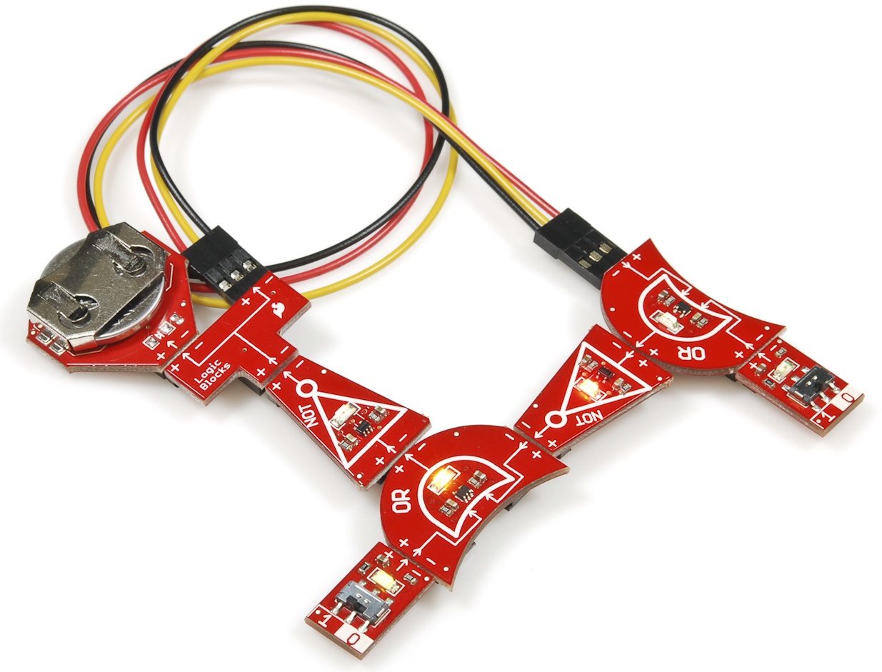
7. 2-to-1 Multiplexer
A multiplexer (or mux) is a common digital circuit used to mix a lot of signals into just one. If you want multiple sources of data to share a single, common data line, you’d use a multiplexer to run them into that line. Multiplexers come in all sorts of shapes and sizes, but they’re all made out of logic gates.
Every multiplexer has at least one select line, which is used to select which input signal gets relayed to the output. In a 2-to-1 multiplexer, there’s just one select line. More inputs means more select lines: a 4-to-1 multiplexer would have 2 select lines, an 8-to-1 has 3, and so on (2n inputs requires n select lines).
Think of a mux as a "digital switch". The select line is the throw on the switch, it chooses which of the many inputs get to be the output.
Here’s how you might make a 2-to-1 multiplexer out of logic gates. A and B are the two inputs, X is the select input, and Y is the output.
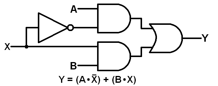
Here's what a truth table would look like for such a circuit:
| Select Input (X) | Input A | Input B | Output Y |
|---|---|---|---|
| 0 | 0 | 0 | 0 |
| 0 | 0 | 1 | 0 |
| 0 | 1 | 0 | 1 |
| 0 | 1 | 1 | 1 |
| 1 | 0 | 0 | 0 |
| 1 | 0 | 1 | 1 |
| 1 | 1 | 0 | 0 |
| 1 | 1 | 1 | 1 |
LogicBlock time!
What You'll Need
- 2x AND Blocks
- 1x OR Block
- 1x Inverter Block
- 1x Splitter Block
- 3x Input Blocks
- 1x Feedback Cable
- 1x Power Block
LogicBlocks Layout
Follow the layout below to create a 2-to-1 multiplexer (Hint: pay more attention than we did to matching up the + and − labels!):

We'll need to internally label each of the inputs. The selector input (X) is the lonely input running into the NOT gate. The remaining two inputs are our A and B, which you can arbitrarily name as you wish.
The output of this multiplexer is indicated by the yellow LED on the OR gate.
The Experiment
Give this order of operations a try:
- Initial state: set all three inputs to 0. The output should be 0.
- Flip A to 1. Nothing should happen to the output, since, with the selector switch set to 0, the B input is being fed into the output.
- Toggle the B input to 1. Observe the output, and set B back to 0. The output should follow your toggling on B!
- Switch the selct to 1. The output should now follow the A input, and it won't care what B is set to.
- Is this circuit combinational or sequential? (Don't let the "Feedback" cable fool you!)
- Can you imagine what a 4-to-1 multiplexer might look like? It'd require double the inputs lines -- two selectors and four possible inputs. Here's a (color-coded) schematic for a 4-to-1 multiplexer:
![]()
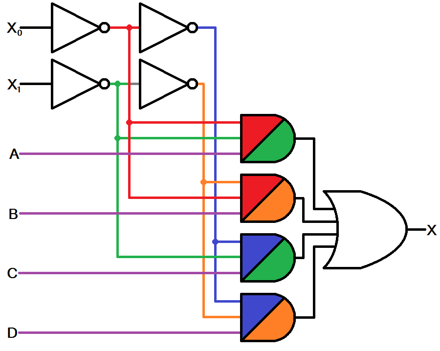
A 4-to-1 demux requires four 3-input ANDs, four NOTs, and one 4-input OR. This circuit allows us to choose to send either A, B, C, or D into the X output. X0 and X1 do the selecting.
- How many gates do you think a 8-to-1 multiplexer might require?
8. 1-to-2 Decoder (De-Multiplexer)
The opposite of a multiplexer is a de-multiplexer, also called a demux or decoder. A demux allows a single input line to be passed through to multiple output lines, again using a select line to choose which output the input goes to.
The schematic for a 2-to-1 demultiplexer looks like this:
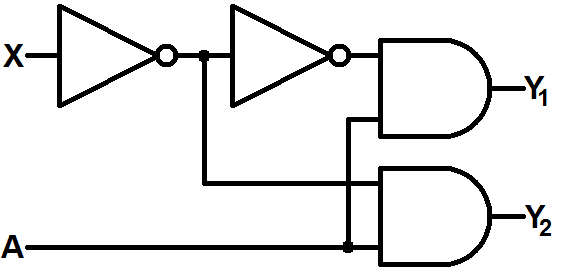
There are two inputs (X and A) and two outputs Y1 and Y2. X is our selector input, it decides which of the two outputs the A input is routed to. When X is 0, the output at Y2 mirrors A (while Y1 will always be 0). When X is 1, the A input is routed to Y1.
The demultiplexer becomes really handy when we have limited outputs available in our system and we need to interface with many many input devices.
What You'll Need
- 2x AND Blocks
- 2x NOT Blocks
- 2x Input Blocks
- 2x Splitter Blocks
- 1x Power Block
- 1x Feedback Cable
LogicBlocks Layout
Construct the LogicBlocks circuit as shown below. Use the feedback cable to simply extend the output of one splitter (you'll need to fuss with it a bit to fit it into both blocks).
In this LogicBlock circuit, our selector input (X) is represented by the Input Block that runs into the NOT Block. The only remaining input is our A input.
The two outputs are each represented by the blue LEDs on each of the AND gates. Y1 is the AND Block without the Power Block attached.
The Experiment
Give this order of operations a try:
- Flip the selector input (X) to 0. Then try toggling the A input both high and low. Only one of the AND Blocks should change, and it should be the same value as the input.
- Flip the X input to 1. Again toggle A a few times. Now the other AND gate should be keeping pace with A.
- Can you imagine what a larger demux might look like? Here's an example circuit for a 2-to-4 decoder:
![]()
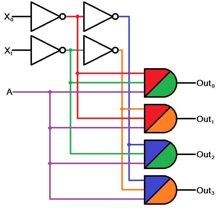
This circuit has two selector inputs (X0 and X1) which route our input (A) to one of the four outputs.
- Compare the 2-to-4 decoder to a 4-to-1 multiplexer (from the last experiment). How do they differe?
- Can you imagine what a circuit for a 3-to-8 decoder might look like?
9. XOR Gate
Up till now, you've been happily living in a world with just three fundamental logic gates. It's time to shatter that perception! Prepare for the revelation that is...the exclusive OR.
An exclusive OR, shortened to XOR, is similar to an OR gate with one major difference. Can you tell from the truth table?:
| Input A | Input B | Output |
|---|---|---|
| 0 | 0 | 0 |
| 0 | 1 | 1 |
| 1 | 0 | 1 |
| 1 | 1 | 0 |
When we say exclusive, we mean it. An XOR only produces a 1 when a lone input is also 1. If two or more inputs are 1, the XOR gate outputs a 0.
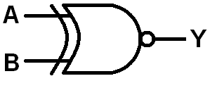
It turns out the XOR gate is an incredibly useful function in digital logic. So useful, in fact, that it gets its own circuit symbol -- kind of a modified OR gate, with a concave line preceding the gate we're used to:
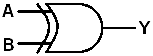
Like all of the previous experiments, the XOR gate can be implemented with the three fundamental digital logic gates. A mix of NOTs, ANDs, and an OR:
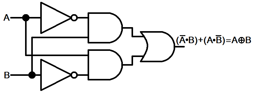
Let's LogicBlock it!
What You'll Need
- 2x AND Blocks
- 1x OR Block
- 2x NOT Blocks
- 2x Input Blocks
- 2x Splitter Blocks
- 1x Power Block
- 1x Feedback cable
LogicBlocks Layout
Construct the XOR as shown below:
The output of the XOR LogicBlocks circuit is represented by the yellow LED on the final OR gate.
The Experiment
Prove the XOR truth table true by toggling both inputs. The LED on the OR block should only light up when you have one or the other of the inputs on.
- Is the XOR a combinational or sequential circuit?
- Can you think of a real life example where a statement is true if only one of the inputs is also true?
Sub-Experiments
Remember NAND and NOR? Well XOR has it's own complement...XNOR. Like the other two negative gates, XNOR has its own bubbled circuit diagram:
The truth table for the 2-input XNOR looks like this:
| Input A | Input B | Output |
|---|---|---|
| 0 | 0 | 1 |
| 0 | 1 | 0 |
| 1 | 0 | 0 |
| 1 | 1 | 1 |
What's really neat about the XNOR is it only proves true when both inputs are the same. That's why we call this operator the logical equality. You could even use the equals sign (=) as the XNOR operator. The equality operator is used all over electronics and programming. If you ever need to check if two statements are equal, an XNOR will be involved.
Hey we've got another NOT Block lying around, let's make an XNOR LogicBlocks circuit! Replace the Power Block with a NOT Block, and plug the Power Block into the end of that.
The output of this circuit is represented by the red LED on the final NOT Block.
- Try toggling both Input Blocks. Does the output LED only illuminate when they're both equal?
Logic Beyond LogicBlocks...
These experiments have barely covered the tip of the proverbial iceberg. We've discovered a lot of fundamental electronics building blocks, but there are many left to uncover. Unfortunately, with the standard kit we've run out of blocks. Here are a few of the foundational circuits and concepts we'd be remiss if we didn't discuss:
Adders
Adders are actual circuits (as opposed to the snakes) that add numbers, and they're built with logic gates! A half-adder is the most simple adder circuit there is. It adds two bits together and has two outputs: the sum (S) and a carry (C). As you can see, the circuit isn't all that complicated:
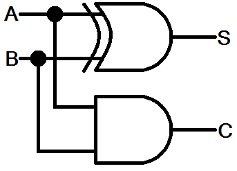
The sum of the two bits is just their XOR, and if both A and B are 1 we generate a carry output.
More complete adders, called full-adders, also have a carry input. These circuits can be strung together in long chains to create a multi-bit binary adder.
Most processors have a block of circuitry within them called an arithmetic logic unit (ALU), where all of the addition, subtraction, multiplication, and division operations are performed. The ALU houses hundreds of adder circuits (among others), and links them to create enormous 32- or 64-bit adders.
Flip-Flops (Latches)
We talked about flip-flops in the SR Latch experiment, but we only glossed over the importance of these circuits. The SR latch we made is one of the more simple latches in electronics. We can modify the SR latch to create a D latch:
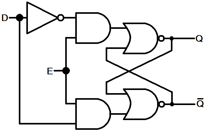
Notice the SR latch in there? The D latch has two inputs -- data (D) and enable (E). As long as the enable input is 1, the Q output will be whatever D is. If enable goes low, Q will retain its set value regardless of what the data input does.
Another popular latch is the JK latch. This latch is also based on the SR latch, but it modifies that "illegal" set of inputs (the one where Q and Q were equal) to instead toggle the current output. Here's how the JK latch is built:
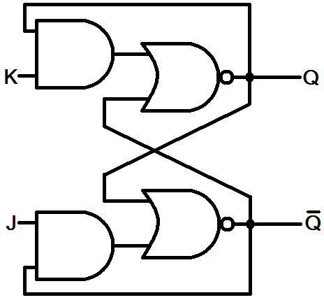
The truth table for a JK latch looks something like this:
| J | K | Previous Q | Current Q |
|---|---|---|---|
| 0 | 0 | 0 | 0 (hold state) |
| 0 | 0 | 1 | 1 (hold state) |
| 0 | 1 | X (don't care) | 0 (reset) |
| 1 | 0 | X | 1 (set) |
| 1 | 1 | 0 | 1 (toggle) |
| 1 | 1 | 1 | 0 (toggle) |
Now, let's turn that JK latch into a JK flip-flop. Flip-flops are usually created by adding a clock input to a latch. A flip-flop with a clock input will usually only perform an operation on the rising edge of a clock signal. The clock input can be used in many ways, for instance multiple flip flops can be synchronized by sharing a clock input. By replacing those 2-input AND gates with a 3-input variety, we can add a clock input to the JK flip-flop:
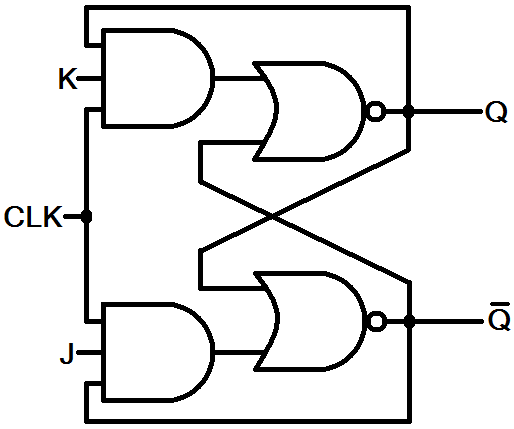
Now, the JK flop-flop will only produce a new output when the clock input is high. This gives us a bit more control over the operation of the flip-flop.
The JK flip-flop will come in handy in the next section...counters.
Counters
Adders add and counters count. Counters are a key element in most processors, especially in timing applications. Your digital clock has to count seconds somehow, right?
A really simple counter can be created by linking together numerous JK flip-flops. If multiple JK flip-flops are all set to constantly toggle (J=K=1), and we link the output of one flip-flop to the input of the next, we can create an asynchronous ripple counter. Here's how we might make a 3-bit ripple counter out of JK flip-flops:
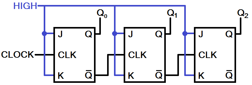
Q0, Q1, and Q2 are our three outputs; Q0 the least-significant bit, Q2 most. With three bits, this circuit can count all the way from 0 to 7 in binary. We can apply a periodic clock to the initial clock input, and begin the counting. Every rising edge on the clock leads to an increment on the counter. Since we've hooked up the complemented output from one JK to the clock input of the next, the Q outputs will toggle whenever the previous one falls.
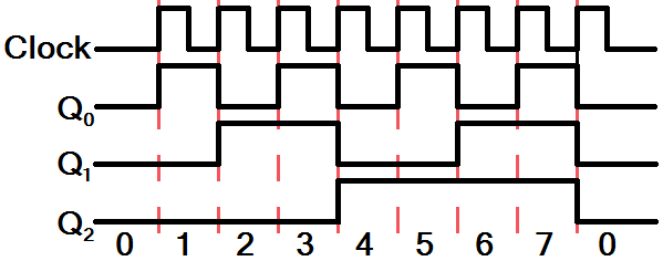
This 3-bit counter will overflow at 7, but adding more flip-flops will increase the upper limit by powers of 2 (n flip-flops count to 2n-1), so we'd need 20 flip-flops to count above 1 million.
There are other types of counters, but this is a good example built with logic circuits that aren't actually all that far-stretched from what we've learned so far.
7400 Series Logic Chips
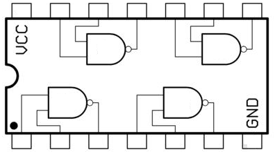
If you're looking for somewhere to go after LogicBlocks, we'd recommend looking into 7400 series logic chips. The 7400s are a huge range of integrated circuits (ICs) that implement all sorts of digital logic functions. You can find quad-NAND gates, along with a variety of other standard digital logic gates. In fact, the chips on the LogicBlock Gate blocks are 7400-series parts -- little single-circuit SMD versions.
Flip flops, counters, multiplexers, decoders, all sorts of other circuits we've covered in this tutorial are implemented in a 7400 series chip. Even more complicated circuits like entire 4-bit ALUs, memories, comparators...seriously, it's a pretty long list, check this out.
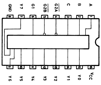
Most 7400 series chips come in a breadboard-friendly DIP package, like the 3-to-8 decoder below (74238). So you can experiment and explore without having to actually solder anything.
If you still can't get enough digital logic, CPLDs (compact programmable logic devices) or even FPGAs (field programmable gate array) would be the next step. They represent a giant leap in complexity from even the 7400 series chips, but those ICs can pack thousands of configurable digital logic circuits into a tiny space. There's a lot of digital logic out there for you to explore, but I hope the LogicBlocks have been a good introduction.
================== End

 浙公网安备 33010602011771号