
【协议时序】- SPI-READ读操作-实验
分析
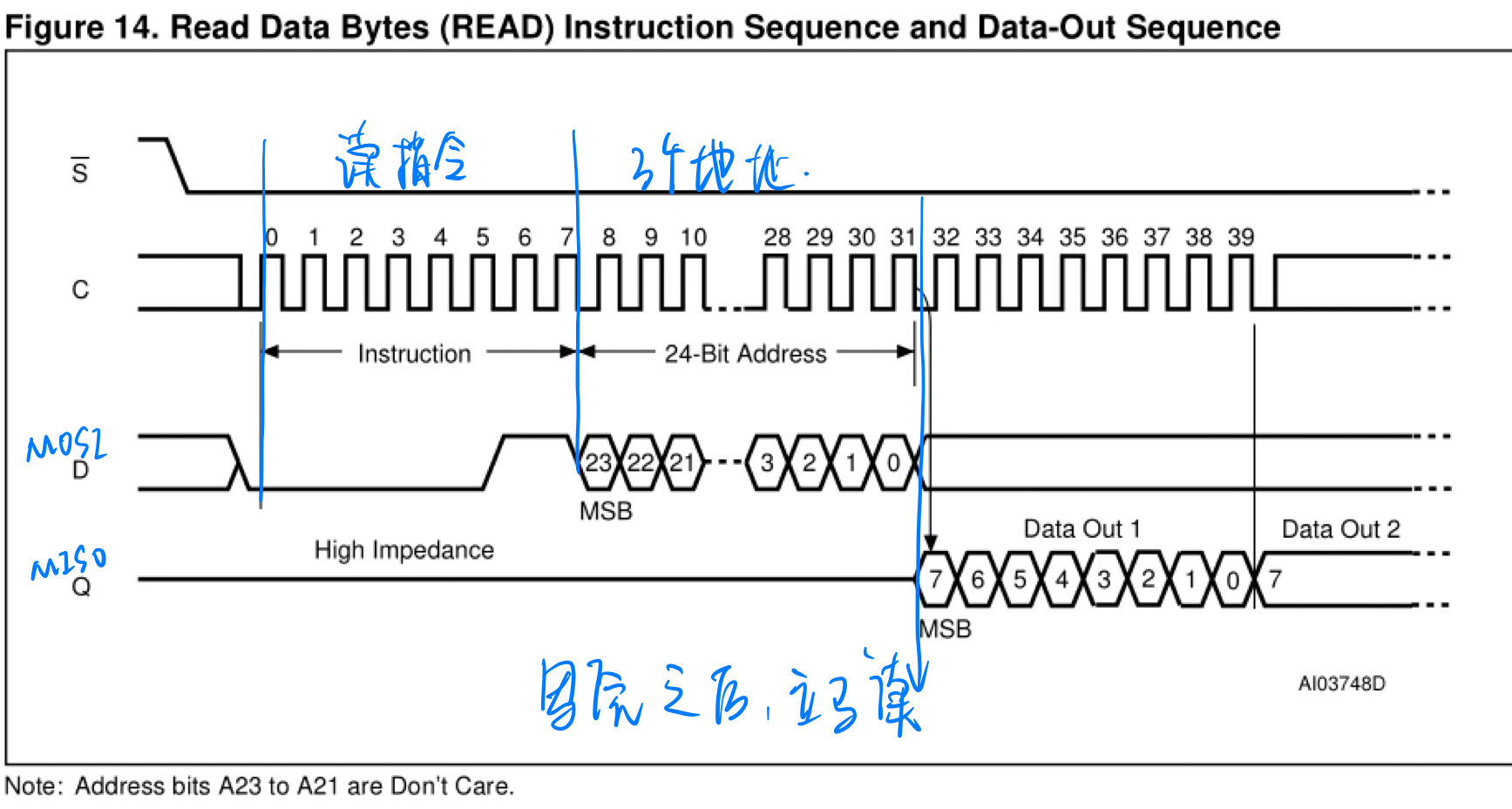
首先需要注意的是,读操作是在SCK上升沿更新数据,写操作是在SCK下降沿更新数据
该实验的具体流程如下:
通过W_R 控制驱动模块处于读操作还是写操作,在写指令和3字节的地址部分,SPI驱动模块处于写操作,
当第三个字节的地址传输完成后,进入读操作去读取Flash传回的数据
时序图
一、设计文件
读指令模块
`timescale 1ns / 1ps
//////////////////////////////////////////////////////////////////////////////////
// Company:
// Engineer:
//
// Create Date: 2022/05/11 21:17:39
// Design Name:
// Module Name: SPI_READ
// Project Name:
// Target Devices:
// Tool Versions:
// Description:
//
// Dependencies:
//
// Revision:
// Revision 0.01 - File Created
// Additional Comments:
//
//////////////////////////////////////////////////////////////////////////////////


module SPI_READ(
    input clk,
    input rst_n,
    input READ_start,
    input read_done,
    input write_done,
    input [7:0]data_read,

    output reg spi_start,
    output reg spi_end,
    output reg W_R,
    output reg [7:0] data_write

    );
    // 状态
    parameter IDLE_S = 3'b001,
              READ_S = 3'b010,
              DRR_S = 3'b100;
    // 指令
    parameter READ = 8'b0000_0011,
              DRR_01 = 8'b0000_0000,
              DRR_02 = 8'b0000_0000,
              DRR_03 = 8'b0000_0000;

    // 状态机
    reg [2:0] state;
    reg [2:0] next_state;

    // 计数器
    reg [7:0] byte_cnt;

always @(posedge clk or negedge rst_n) begin
    if(!rst_n)
        byte_cnt <= 8'd0;
    else if(write_done)begin
        case(state)
            IDLE_S: byte_cnt <= 8'd0;
            READ_S: byte_cnt <= 8'd0;
            DRR_S:
                if(byte_cnt == 8'd2)
                    byte_cnt <= 8'd0;
                else
                    byte_cnt <= byte_cnt + 8'd1;
            default:byte_cnt <= 8'd0;
        endcase

    end

end

always @(posedge clk or negedge rst_n) begin
    if(!rst_n)
        state <= IDLE_S;
    else
        state <= next_state;
end

always @(*) begin
    case(state)
    IDLE_S:
        if(READ_start)
            next_state <= READ_S;
        else
            next_state <= IDLE_S;
    READ_S:
        if(write_done && byte_cnt == 8'd0)
            next_state <= DRR_S;
        else
            next_state <= READ_S;
    DRR_S:
        if(write_done && byte_cnt == 8'd2)
            next_state <= IDLE_S;
        else
            next_state <= DRR_S;
    default: next_state <= IDLE_S;
    endcase

end

// 输出信号
always @(posedge clk or negedge rst_n) begin
    if(!rst_n)
        spi_start <= 1'b0;
    else if(state == IDLE_S && next_state == READ_S)
        spi_start <= 1'b1;
    else
        spi_start <= 1'b0;
end

always @(posedge clk or negedge rst_n) begin
    if(!rst_n)
        spi_end <= 1'b0;
    else if(state == DRR_S && next_state == IDLE_S && read_done)
        spi_end <= 1'b1;
    else
        spi_end <= 1'b0;
end

always @(posedge clk or negedge rst_n) begin
    if(!rst_n)
        W_R <= 1'b0;
    else if(READ_start)
        W_R <= 1'b1;
    else if(state == DRR_S && next_state == IDLE_S)//state == DRR_S && next_state == IDLE_S
        W_R <= 1'b0;
end

always @(*) begin
    case(state)
        IDLE_S: data_write <= 8'd0;
        READ_S: data_write <= READ;
        DRR_S:
        case(byte_cnt)
            8'd0: data_write <= DRR_01;
            8'd1: data_write <= DRR_02;
            8'd2: data_write <= DRR_03;
            default: data_write <= 8'd0;
        endcase
        default: data_write <= 8'd0;
endcase
end

endmodule
SPI驱动模块
`timescale 1ns / 1ps
//////////////////////////////////////////////////////////////////////////////////
// Company:
// Engineer:
//
// Create Date: 2022/04/29 21:51:51
// Design Name:
// Module Name: SPI
// Project Name:
// Target Devices:
// Tool Versions:
// Description:
// SPI驱动模块,工作在模式0,即SCK空闲状态为低电平,SCK下降沿更新MOSI的数据,MSB
// Dependencies:
//
// Revision:
// Revision 0.01 - File Created
// Additional Comments:
//
//////////////////////////////////////////////////////////////////////////////////


module SPI_drive_my(

input           clk             ,
input           rst_n           ,
input           spi_start       ,
input           spi_end         ,
input   [7:0]   data_write         ,
input           W_R             ,//判断模块工作模式:读、写

input             spi_MISO        ,
output    reg      spi_SCK         ,
output    reg      spi_CE          ,
output    reg     spi_MOSI        ,

output  reg        read_done        ,
output  reg        write_done         ,
output  reg [7:0]   data_read

    );
// 定义状态机
parameter IDLE = 3'b001,
          WR = 3'b010,
          RD = 3'b100;
reg     [2:0]       state       ;
reg     [2:0]       next_state  ;

//定义计数器
reg     [1:0]       cnt_4      ;
reg     [3:0]       cnt_8       ;
parameter           MAX_CNT_4  =   3        ,
                    MAX_CNT_8   =   7       ;

always@(posedge clk or negedge rst_n)begin
    if(!rst_n)
        state <= IDLE     ;
    else
        state <= next_state     ;
end

always @(*) begin
    case(state)
        IDLE:
            if(spi_start == 1'b1 && W_R == 1'b0)
                next_state <= RD  ;
            else if(spi_start == 1'b1 && W_R == 1'b1)
                next_state <= WR  ;
        RD:
            if(spi_end)
                next_state <= IDLE  ;
            else if(cnt_4 == 2'd0 &&  cnt_8 == 8'd0) begin
                    if(W_R == 1'b0)
                        next_state <= RD  ;
                    else
                        next_state <= WR  ;

            end
        WR:
            if(spi_end)
                next_state <= IDLE  ;
            else if(cnt_4 == 2'd0 &&  cnt_8 == 8'd0) begin
                    if(W_R == 1'b0)
                        next_state <= RD  ;
                    else
                        next_state <= WR  ;

            end
            default:next_state <= IDLE  ;
    endcase
end

// 计数器
// SCK时钟计数器
always@(posedge clk or negedge rst_n)begin
    if(!rst_n)
        cnt_4  <=  2'd0   ;
    else if(state != IDLE)
        cnt_4  <=  cnt_4  +   2'd1   ;
end

always@(posedge clk or negedge rst_n)begin
    if(!rst_n)
        cnt_8 <= 8'd0;
    else if(cnt_4 == MAX_CNT_4)begin
            cnt_8 <= cnt_8 + 8'd1;
        if(cnt_8 == MAX_CNT_8)
            cnt_8 <= 8'd0;
    end

end

always@(posedge clk or negedge rst_n)begin
    if(!rst_n)
        spi_SCK <= 1'd0;
    else if(cnt_4 == 2'd0 && state != IDLE)
        spi_SCK <= 2'd0;
    else if(cnt_4 == 2'd2 && state != IDLE)
        spi_SCK <= 1'd1;
end

always@(posedge clk or negedge rst_n)begin
    if(!rst_n)
        spi_CE <= 1'b1;
    else if(spi_start == 1'b1)//SPI开始工作
        spi_CE <= 1'b0;
    else if(next_state == IDLE && cnt_8 == MAX_CNT_8 || spi_end)//SPI结束工作
        spi_CE <= 1'b1;
    else
        spi_CE <= spi_CE;
end

always@(posedge clk or negedge rst_n)begin
    if(!rst_n)
        spi_MOSI <= 1'b0;
    else if(!spi_CE && cnt_4 == 2'd0)//0模式、BSM
        spi_MOSI <= data_write[7-cnt_8];
    else if(spi_CE)
        spi_MOSI <= 1'b0;
    else
        spi_MOSI <= spi_MOSI;
end
// 发送数据完成-标志位
always@(posedge clk or negedge rst_n)begin
    if(!rst_n)
        read_done <= 1'b0;
    else if(cnt_4 == 2'd3 && cnt_8 == 3'd7 && state == RD)
        read_done <= 1'd1;
    else
        read_done <= 1'b0;
end
// 接收数据完成-标志位
always@(posedge clk or negedge rst_n)begin
    if(!rst_n)
        write_done <= 1'b0;
    else if(cnt_4 == 2'd2 && cnt_8 == 3'd7 && state == WR)
        write_done <= 1'd1;
    else
        write_done <= 1'b0;
end

always@(posedge clk or negedge rst_n)begin
    if(!rst_n)
        data_read <= 8'd0;
    else if(cnt_4 == 2'd2 && state == RD)
        data_read[7-cnt_8] <= spi_MISO;
    else
        data_read <= data_read;
end


endmodule
顶层模块
`timescale 1ns / 1ns
//////////////////////////////////////////////////////////////////////////////////
// Company:
// Engineer:
//
// Create Date: 2022/05/11 22:12:52
// Design Name:
// Module Name: top_SPI_READ
// Project Name:
// Target Devices:
// Tool Versions:
// Description:
//
// Dependencies:
//
// Revision:
// Revision 0.01 - File Created
// Additional Comments:
//
//////////////////////////////////////////////////////////////////////////////////


module top_SPI_READ(
    input clk,
    input rst_n,
    input READ_start,
    input spi_MISO,

    output spi_SCK,
    output spi_CE,
    output spi_MOSI

);

wire spi_start,spi_end,W_R,read_done,write_done;
wire [7:0] data_write;
wire [7:0] data_read;

SPI_drive_my SPI_drive_my_inst
(

.clk(clk)             ,
.rst_n(rst_n)           ,
.spi_start(spi_start)       ,
.spi_end(spi_end)         ,
.data_write(data_write)         ,
.W_R(W_R)             ,

.spi_MISO(spi_MISO)        ,
.spi_SCK(spi_SCK)         ,
.spi_CE(spi_CE)          ,
.spi_MOSI(spi_MOSI)        ,

.read_done(read_done)        ,
.write_done(write_done)         ,
.data_read(data_read)

    );

SPI_READ SPI_READ_inst
(
.clk(clk),
.rst_n(rst_n),
.READ_start(READ_start),
. read_done(read_done),
.write_done(write_done),
.data_read(data_read),

.spi_start(spi_start),
.spi_end(spi_end),
.W_R(W_R),
.data_write(data_write)

    );

endmodule
二、测试文件
`timescale 1ns / 1ps
//////////////////////////////////////////////////////////////////////////////////
// Company:
// Engineer:
//
// Create Date: 2022/05/11 22:28:58
// Design Name:
// Module Name: tb_top_SPI_READ
// Project Name:
// Target Devices:
// Tool Versions:
// Description:
//
// Dependencies:
//
// Revision:
// Revision 0.01 - File Created
// Additional Comments:
//
//////////////////////////////////////////////////////////////////////////////////


module tb_top_SPI_READ();

reg clk,rst_n,READ_start,spi_MISO;
wire spi_SCK,spi_CE,spi_MOSI;

initial begin
    clk = 1'b0;
    rst_n = 1'b0;
    READ_start = 1'b0;
    spi_MISO <= 1'b0;

    #80
    rst_n = 1'b1;
    READ_start = 1'b1;
    #20
    READ_start = 1'b0;

    wait(top_SPI_READ_inst.SPI_READ_inst.state == top_SPI_READ_inst.SPI_READ_inst.DRR_S
            && top_SPI_READ_inst.SPI_READ_inst.next_state == top_SPI_READ_inst.SPI_READ_inst.IDLE_S)
    @(negedge spi_SCK);
    spi_MISO <= 1'b0;
    @(negedge spi_SCK);
    spi_MISO <= 1'b1;
    @(negedge spi_SCK);
    spi_MISO <= 1'b0;
    @(negedge spi_SCK);
    spi_MISO <= 1'b0;
    @(negedge spi_SCK);
    spi_MISO <= 1'b0;
    @(negedge spi_SCK);
    spi_MISO <= 1'b0;
    @(negedge spi_SCK);
    spi_MISO <= 1'b1;
    @(negedge spi_SCK);
    spi_MISO <= 1'b1;
end

always #10 clk = ~ clk;


top_SPI_READ top_SPI_READ_inst
(
.clk(clk),
.rst_n(rst_n),
.READ_start(READ_start),
.spi_MISO(spi_MISO),

.spi_SCK(spi_SCK),
.spi_CE(spi_CE),
.spi_MOSI(spi_MOSI)
);
endmodule
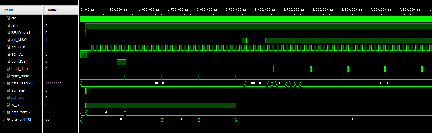
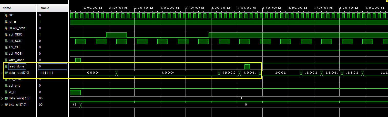
三、波形图

 浙公网安备 33010602011771号