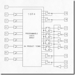
PLD
PLD:
A programmable logic device is an electronic component used to build reconfigurable digital circuits. Unlike integrated circuits(IC) which conist of logic gates and have a fixed function, a PLD has an undefined function at the time of manufacture. Before the PLD can be used in a circuit it must be programmed (reconfigured) by using a specialized program.
Early programmable logic:
1969-XC157(Motorola), a mask-programmable gate array with 12 gates and 30 uncommitted input/output pins.
1970-TI developed a mask-programmable IC based on the IBM read-only memory associative memory or ROAM.--TMS2000(17inputs and 18 outputs with 8 JK flip flop)
1971-General Electric Company was developing a programmable logic device based on the new PROM technology.
1973-DM7575(National Semiconductor)----with no memory registers with 14 inputs and 8 outputs.
1974-MMI(Monolithic Memories)
PLA:(1970—TI)
PLAs differ from programmable Array Logic devices(PALs and GALs) in that both AND and OR gate planes are programmable.
Implementation procedure:
1preparation in SOP(sum of products) form
2Obtain the minimum SOP form to reduce the number of product terms to a minimum.
3Decide the input connection of the AND matrix for generating the required product term.
4Then decide the input connections of OR matrix to generate the sum terms
5Decide the connections of invert matrix.
6Program the PLA.
PAL:(1978-MMI)
PAL architecture:
the PAL architecture consists of two main components : a logic plane and output logic macrocells.
programmable logic plane is a programmable read-only memory(PROM) array .
fixed-OR, programmable-AND
GALs:(Lattice Semiconductor )
Generic Array Logic
innovation of the PAL
CPLDs:
Some of the CPLD features are in common with PALs:
Non-volatile configuration memory. Unlike many FPGAs, an external configuration ROM isn't required, and the CPLD can function immediately on system start-up.
For many legacy CPLD devices, routing constrains most logic blocks to have input and output signals connected to external pins, reducing opportunities for internal state storage and deeply layered logic. This is usually not a factor for larger CPLDs and newer CPLD product families.
Other features are in common with FPGAs:
Large number of gates available. CPLDs typically have the equivalent of thousands to tens of thousands of logic gates, allowing implementation of moderately complicated data processing devices. PALs typically have a few hundred gate equivalents at most, while FPGAs typically range from tens of thousands to several million.
Some provisions for logic more flexible than sum-of-product expressions, including complicated feedback paths between macro cells, and specialized logic for implementing various commonly used functions, such as integer arithmetic.
The most noticeable difference between a large CPLD and a small FPGA is the presence of on-chip non-volatile memory in the CPLD, which allows CPLDs to be used for "boot loader" functions, before handing over control to other devices not having their own permanent program storage. A good example is where a CPLD is used to load configuration data for an FPGA from non-volatile memory
FPGAs:
How PLDs retain their configuration:
A PLD is a combination of a logic device and a memory device.
The memory is used to store the pattern that was given to the chip during programming. Most of the methods for storing data in an integrated circuit have been adapted for use in PLDs.
These include:Silicon antifuses(反熔丝)、SRAM、EPROM\EEPROM、Flash memory
PLD programming languages:
JEDEC files
HDLs
VHDL、Verilog
PALASM、ABEL、CPUL


 浙公网安备 33010602011771号