有趣的Cache创新@HotChips'33
姚伟峰
当前流行的计算架构(包括CPU、GPU等)大多数还是follow冯-诺依曼架构(如下)。
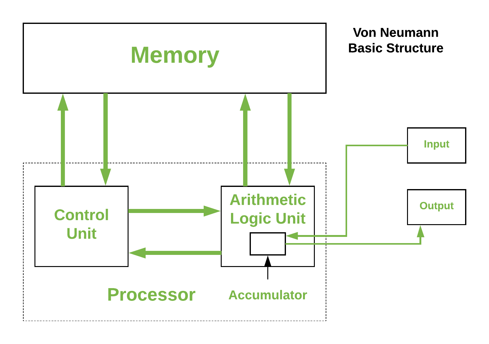
冯-诺依曼体系结构用(processor,memory,IO)三元组建模计算架构,三者配合开展工作,因此会受到短板效应的影响,一般叫冯-诺伊曼bottleneck。随着工艺技术和应用(如AI等计算密集型应用)的推进,行业在processor的计算能力上取得了摩尔以及超摩尔的进展,而memory的进展以density为主,在带宽上远远没赶上processor的脚步。
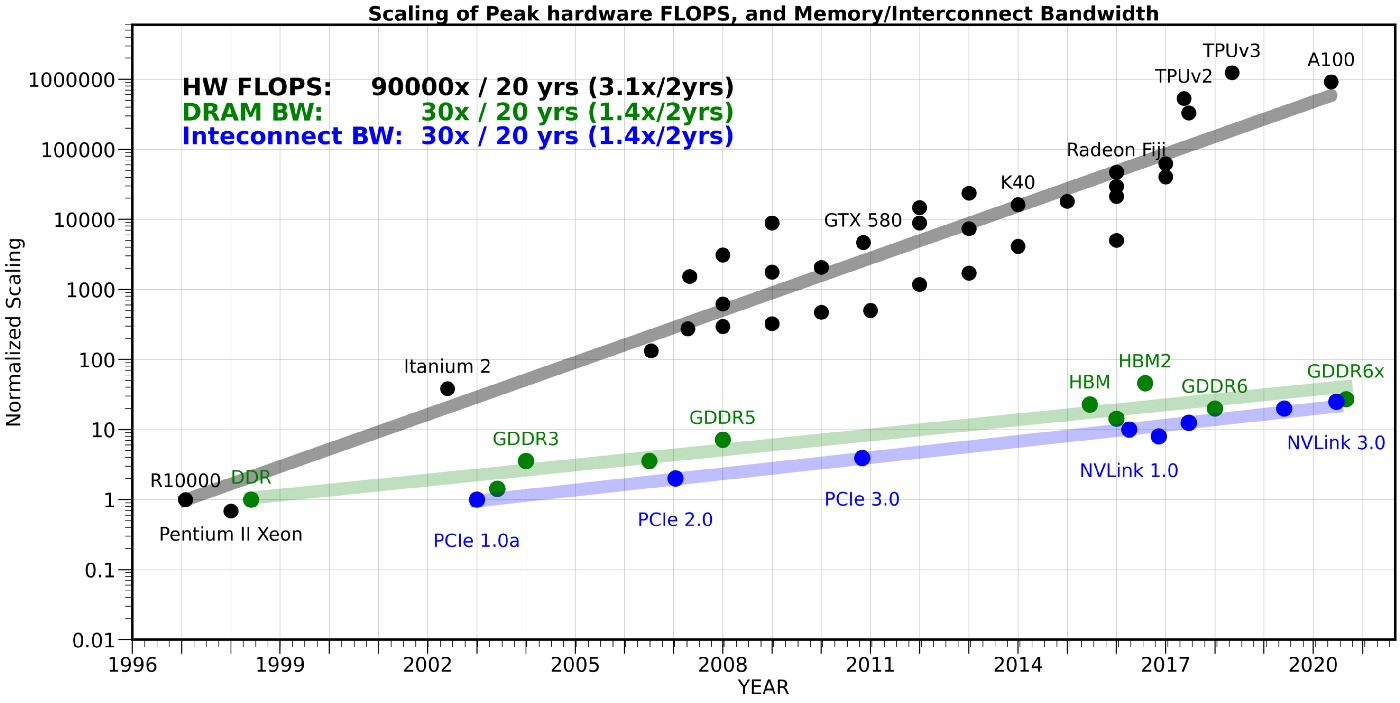
下面这个图告诉我们:HW FLOPS 20年提高了90,000倍,而memory带宽仅有30倍,连脚拇指都没摸上。因此,memory带宽越来越成为冯-诺依曼结构释放系统性能的瓶颈,称为memory wall。
冯-诺依曼系统在设计时其实已经加入了memory hierarchy,来缓解memory wall:
基于这个hierarchy继续缓解memory wall有两种方法:
-
提高memory带宽。这个近几年在HBM->HBM2->HBM3的演进中有所进展,但仍不能独力满足需求。
-
提高memory access的cache bound,充分利用cache的高带宽优势。提高cache bound对算法、系统、微架构都有一定的要求,这里只谈对微架构的要求,主要是提高cache的capacity。
知易行难,由于Moore定律的放缓,使得增加die size或者减少逻辑电路面积变得越来越难,因此暂时堵住了暴力增加on-die SRAM来增加cache capacity的路。
从HotChips’33 CPU track的presentations来看,工业界花了很多心思在如何解决这个问题上,innovate more on Cache than IPC(Instructions Per Cycle)。AMD,Intel,IBM都提出了自己的方法。
AMD - Zen 3
V-Cache(Vertical Cache)
V-Cache expands L3 cache size through advanced package innovation, since the slow-down of Moore’s Law makes increasing die sizes and/or shrinking logic circuits hard.
具体示意图如下:
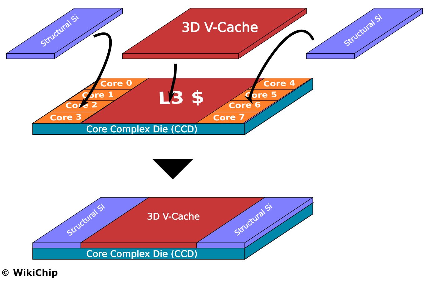
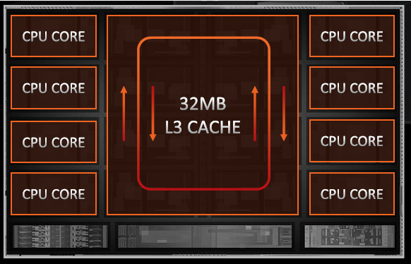
通过V-Cache封装技术,L3$的capacity得到了增加:
-
per CCD(Core Complex Die)
32 MiB L3 Cache + 64 MiB V-Cache = 96 MiB -
per core
96 / 8 MiB = 12 MiB
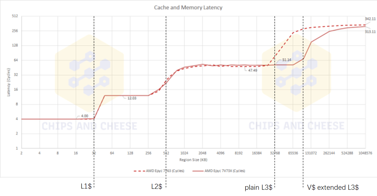
Chips and Cheese测试了V-Cache对data access latency和bandwidth造成的影响。如下:
-
Latency
-
Bandwidth
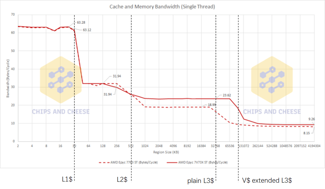
由上述测试数据,可以得到一些观察:
-
V-Cache和on-die的L3 cache是统一编址使用的,因此在on-die L3 cache能cover的区域内,数据访问延时有3~4个cycles的增加,但3~4个cycles是一个很小的数字了。
-
V-Cache增加了cache capacity,减少了32M~256MB大小数据的access latency。且由于增加了cache命中率,增加了数据访问带宽。
L3 Fabric
AMD claim了:bi-directional ring bus, 156.8 GB/s per CCD@4.9GHz.
这个就还好吧,core少的时候采用ring作为NOC感觉算是个公认的practice,没有get到点。
Intel - CPU and GPU
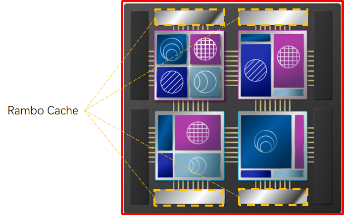
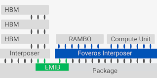
Rambo Cache
Rambo Cache与 V-Cache思路相同,但使用了不同的封装技术。从已公开的资料看,与V-Cache采用cache 3D stacking方法不一样,Rambo Cache使用了2.5D stacking的interposer方法(与HBM与计算器件连接的思路相似),区别是Rambo Cache使用了Foveros Interposer。具体看如下两张图便知:
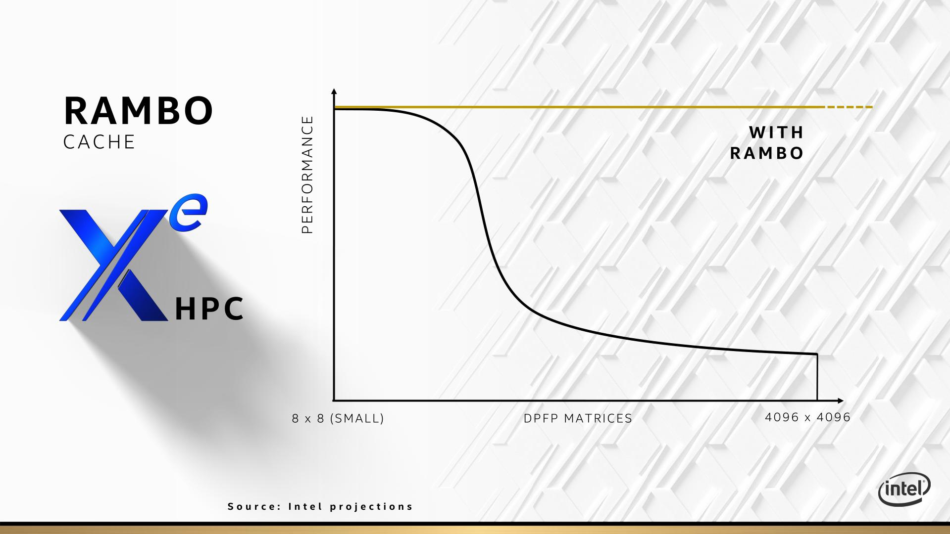
目前尚无公开的Rambo Cache第三方测试数据,只有一张Intel自己展示的projection效果展示。
IBM - Telum
Virtual Cache
AMD和Intel的做法是延续性创新:不改变目前的memory hierarchy组成,通过封装工艺来增大cache size,以解决当前on-die cache size无法增大的问题。
IBM的Virtual Cache玩的是颠覆式创新,想玩一把大的,改变当前L2$和L3$是分离的物理器件的做法。它取消了物理的L3$(及L4$, 若有),而是使用chip内L2$作为virtual L3$,机箱内L2$ virtual cache,妥妥的cache pooling的想法。
具体做法为:
-
首先,直接把L2$ size扩大到32MB,这是别人L3$的size;
-
然后,取消L3$,把同一个chip内的其他cores的L2$作为当前core的L3$;
-
最后,把同一个drawer(即机箱)内的其他chip的cores的 L2$作为当前core的L4$;
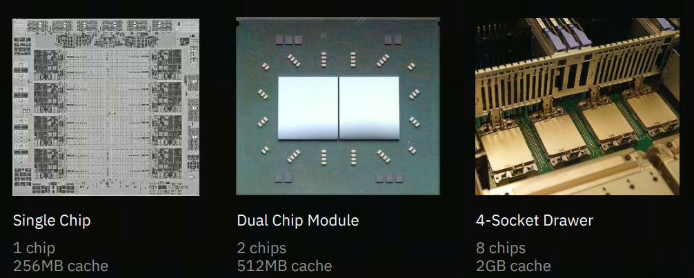
对一个 4-Socket的drawer(如下图所示),每个drawer由4个sockets,每个socket有2个chips, 每个chip有8个cores。
对每个core,有:
-
32MB的private L2$ (19-cycle latency)
-
224MB(32MB * 8 - 32MB)的on-chip shared virtual L3$ (+12ns latency)
-
7936MB(256MB * 8 - 256MB)的off-chip shared virtual L4$
具体spec有:


目前尚无公开的第三方测试数据,IBM自称using this virtual cache system, there is the equivalent of 1.5x more cache per core than the IBM z15, but also improved average latencies for data access. Overall there is a per-socket performance improvement of >40%.
想法很酷,但魔鬼总是在执行细节中,需要时间来告诉我们答案。
References
-
HotChips'33 slides


 浙公网安备 33010602011771号