HDLBits(14)3.1
3 电路
3.2 时序逻辑
3.2.1 锁存器与触发器(Latches and Flip-Flops)
- Dff8ar(DFF with asynchronous reset)
创建 8 位具有高电平有效异步复位的 D 触发器。所有 DFF 都应由clk的上升沿触发。
*同步和异步复位触发器之间代码的唯一区别在于敏感变量
module top_module(
    input clk,
    input areset,
    input [7:0]d,
    out[7 :0]q
);
    always @(posedge clk or posedge areset)begin
        if(areset)
            q<=8'd0;
        else
            q<=d;
    end
endmodule
对于同步复位系统来说,当同步复位事件发生时,等到下一个时钟上升沿才会得到响应,响应的速度较慢
与之相对的异步复位的响应就很快,因为在异步复位有效的时刻,复位响应就会发生
- Dff16e(DFF with byte enable)
创建 16 位D触发器。有时只修改一组触发器的一部分很有用。字节使能(byte-enable)输入控制 16 个寄存器中的每个字节是否应在该周期写入。byteena[1]控制高字节d[15:8],而byteena[0]控制低字节d[7:0]。resetn是一个同步的低电平有效复位。所有 DFF 都应由clk的上升沿触发
module top_module (
    input clk,
    input resetn,
    input [1:0] byteena,
    input [15:0] d,
    output [15:0] q
);
    always @(posedge clk) begin
        if(!resetn)
            q<=16'd0;
        else
            begin
                q[7:0]<=byteena[0]?d[7:0]:q[7:0];
                q[15:8]<=byteena[1]?d[15:8]:q[15:8];
            end
    end
endmodule
- D Latch
实现以下电路:
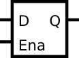
同 D触发器相比,这个元件没有 clk 端口,取而代之的是 ena 端口,所以这是一个锁存器。锁存器的特征在于,相较于 D触发器的触发事件发生于 clk 时钟的边沿,锁存器锁存的触发事件发生于使能端 ena 的电平。
当你成功实现了这个锁存器时,Quartus 会提醒(祝贺)你生成了一个锁存器。锁存器相比触发器会消耗更多的资源,所以综合器会在推断出锁存器时产生提醒,防止开发者在不想使用锁存器时,因为代码风格等原因误产生了锁存器。
module top_module (
    input d,
    input ena,
    output reg q);
    always@(*)begin
        if(ena)begin
            q<=d;
        end
    end
endmodule
module top_module (
input d,
input ena,
output q);
always @(*)
begin
if(ena)
q <= d;
end
endmodule
- DFF
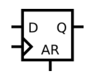
AR 代表 asynchronous reset,所以这是一个带有异步复位的 D 触发。
图中的三角形代表时钟,不再用 CLK 标出。
module top_module (
    input clk,
    input d,
    input ar,   // asynchronous reset
    output reg q);
    always@(posedge clk or posedge ar)begin
        if(ar)begin
        	q <= 1'b0;
        end else begin
            q <= d;
    end
    end
endmodule
module top_module (
input clk,
input d,
input ar, //异步复位
output q);
always @(posedge clk or posedge ar)
begin
if(ar)
q <= 1'b0;
else
q <= d;
end
endmodule
- DFF
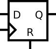
R表示synchronous reset(同步复位)
module top_module (
    input clk,
    input d,
    input r,   // synchronous reset
    output reg q);
    always @(posedge clk) begin
        if(r)
            q <= 1'b0;
        else
            q <= d;
    end
endmodule
- DFF+Gate

module top_module (
    input clk,
    input in,
    output out);
    always @(posedge clk) begin
        out<=in^out;
    end
endmodule
- Mux and DFF
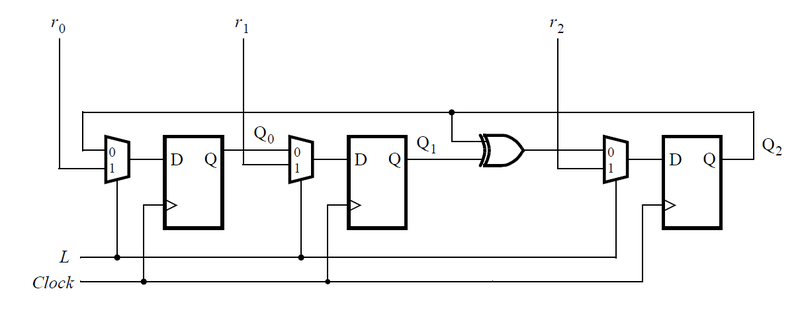
用三个包含触发器和多路选择器的子模块实现图中电路,题目只要求写出包含一个触发器和多路选择器的子模块
module top_module(
    input clk,
    input L,
    input r_in,
    input q_in,
    output reg Q
);
    wire temp;
    assign temp = L?r_in:q_in;
    always @(posedge clk)
        begin
            Q <= temp;
        end
endmodule- Mux and DFF
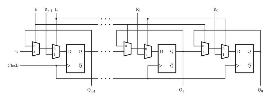
module top_module (
    input clk,
    input w, R, E, L,
    output Q
);
    wire temp1, temp2;
    assign temp1 = E ? w:Q;
    assign temp2 = L ? R:temp1;
    always @ (posedge clk)
        begin
           Q <= temp2;
        end
endmodule- DFF and gates

给定如图所示的有限状态机电路,假设 D 触发器在机器开始之前初始复位为零,建立这个电路。小心复位状态。确保每个 D 触发器的Q非·输出确实是其 Q 输出的倒数,即使在模拟的第一个时钟沿之前也是如此。
module top_module (
    input clk,
    input x,
    output z
);
    reg q1,q2,q3;
    always @(posedge clk) begin
            q1 <= x^q1;
            q2 <= x&(~q2);
            q3 <= x|(~q3);
    end
    assign z = ~(q1|q2|q3);
endmodule

 浙公网安备 33010602011771号