

PWM DAC vs. Standalone
Posted by AnalogAdvocate on April 09, 2010
Design, General
In today’s highly competitive electronics environment, designers are constantly looking for ways to reduce overall system costs. One of the most commonly asked questions that analog specialists at digital microcontroller (MCU) companies hear from customers is, is the almost cost-free Pulse-Width-Modulation (PWM) Digital-to-Analog Converter (DAC) good enough for my application, or do I need a higher-performance, standalone DAC instead?”
The generation of an analog voltage using a digital Pulse-Width-Modulated signal is known as a PWM DAC. As most designers’ PCB boards have a microcontroller with a built-in PWM-output feature onboard, a simple digital-to-analog data conversion can be easily realized by adding a few passive components at the MCU’s PWM-output pin. This is an alternative to using a standalone DAC. In the MCU application environment, system designers can have DAC functionality nearly free of charge. PWM DACs are widely used in very low-cost applications, where accuracy is not a primary concern. Standalone DACs, however, are used for applications requiring higher accuracy.
Although the PWM DAC can be realized with the simple addition of a few passive components, implementing a PWM DAC for system applications is not a simple task. There are many limitations associated with this. Understanding the complexities of using the PWM DAC and its effects can save significant development time and effort. This article presents a technique for converting a PWM pulse to an analog voltage using a simple, RC low-pass filter. This entry also reviews the PWM DAC’s limitations and its key design constraints on resolution, frequency, ripple, settling time and current consumption are discussed, which are very important design parameters that are largely affected by the R and C values, as well as the PWM duty cycle and frequency.
Standalone DACs
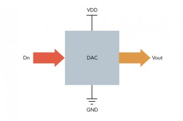
Figure 1 shows an example of a standalone DAC. Its analog output voltage is given by:
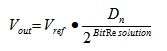
Where Dn is the digital code. For example, with a 12-bit DAC, the user can get Vout = 2.5V with Vref = 5V and Dn = 1000-0000-0000. Typical standalone DAC devices provide good linearity and a short settling time, which is the time required to update each output voltage.
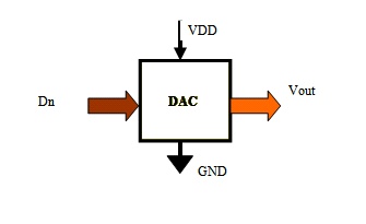
Figure 1 Configuration of Standalone DAC
How PWM DACs Work
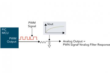
Figure 2 shows a basic configuration of the PWM DAC. The MCU outputs a PWM signal to an RC low pass-filter. The PWM pulse train’s digital value becomes an analog voltage, when it passes through the RC filter. At a given period of time, the analog output is proportional to the PWM pulse’s high durations.

Figure 2 Block Diagram of a PWM DAC
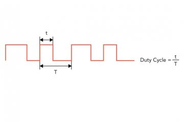
A PWM signal is defined as a digital signal with a fixed frequency, but a varying duty cycle. Figure 3 illustrates a PWM signal. The PWM period (T) is the time interval required to complete one full PWM cycle. The duty cycle is the ratio of the high duration (t) to the total period (T).
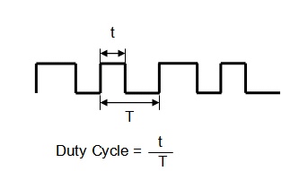
Figure 3 PWM Signal
The PWM signal and RC-filter circuit parameters affect the analog output’s resolution, amplitude, settling time and ripple. The PWM DAC’s limitations are clearly demonstrated by analyzing the interaction of the PWM parameters and the RC filter. A better understanding of the relationship between these parameters enables designers to optimize the PWM to best suit their application’s requirements, while minimizing design time.
PWM DAC Bit Resolution
The PWM counter length (L) and the smallest duty-cycle change in the PWM counter (C) determine the PWM DAC’s bit resolution. The following equation expresses the maximum bit resolution of the PWM DAC:

For example, if the system generates an analog output voltage from a PWM DAC with a counter of 4096 (L) and a minimum count step of one (C), the PWM DAC’s bit resolution is 12-bits.
When the PWM resolution is determined, it is possible to calculate the Least Significant Bit (LSB) size. The LSB size is dependant upon the PWM resolution and the PWM’s output-high level voltage (VOH), and can be calculated using the following equation.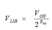
For example, a 12-bit PWM DAC with a VOH of 5V has an LSB size of 1.2mV.
RC Filter Design Considerations for PWM DAC
One key design consideration when determining the PWM’s resolution is output-voltage ripple. Ripple occurs due to overshoot and undershoot as the PWM charges and discharges the RC circuit. One way to approximate the charge characteristics is to modify the equations to charge and discharge an RC-filter circuit. As the effects of this are cumulative, the following equations can be used as approximations.
 (4)
(4) (5)
(5) (6)
(6)
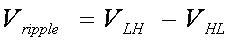
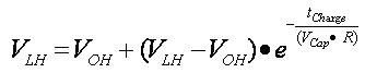
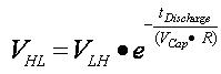
VLH is the voltage increase for a specific PWM period, and VHL is the voltage decrease for a specific PWM period. The values of VLH and VHL are dependant upon not only the RC filter values, but also upon the PWM frequency and duty cycle. The PWM frequency and duty cycle determine the time available for the PWM to charge (tcharge) and discharge (tdischarge) the capacitor. Vripple is the difference between VLH and VHL for the same PWM period.
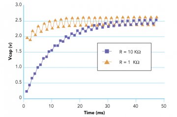
Figure 4 illustrates the magnitude of the voltage ripple across the output capacitor vs. time. The vertical axis displays the magnitude of the ripple voltage, while the horizontal axis provides the corresponding time. The plot shows how the ripple voltage settles at approximately 125 mV in a time interval of approximately 40 ms for R = 10K ohms, and 250 mV at 20 ms for R = 1 K ohm. In the previous example, an LSB size of less than 1.2mV for a 12-bit system was needed. This ripple is greater than 100 LSB for 12-bit DAC with a 5V reference, meaning that the resulting PWM DAC solution has an effective resolution of less than 6 bits due to the ripples.
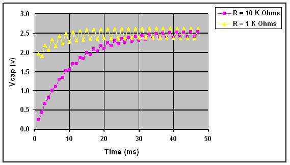
Figure 4: Voltage Ripple Comparison for VOH = 5V, C = 1μF, PWM frequency = 1 kHz, Duty Cycle = 50%
The ripple can be reduced by increasing the capacitor and the resistor values or increasing the PWM frequency. All of these will decrease the ripple’s magnitude.
As shown in Figure 4, the ripple decreases as the resistance value increases. However, nothing comes without a price-the settling time doubles as the ripple decreases by 50 %.
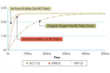
For applications that require faster settling time (increased bandwidth) and higher resolution, one could add a second RC filter. The obvious tradeoffs include the cost of additional components and the increased board space occupied. Figure 5 shows a model for a two-pole RC low-pass filter. Figure 6 shows the analog output voltage of this model.
Figure 5: PSPICE Model for Two-Pole RC Low-Pass Filter
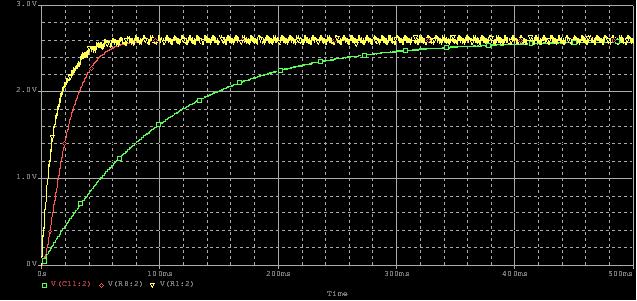
Figure 6: Analog Voltage Output vs. Settling Time of the Two Pole RC Low-Pass Filtere
There are a couple of things to keep in mind when designing the filter. First, make sure that the pole of the RC is set at a much greater frequency than that of the signal being generated. Secondly, if you are designing a two-pole filter, make sure that R2 > R1.
The 3dB corner frequency of the RC filter is given by:
 (7)
(7)
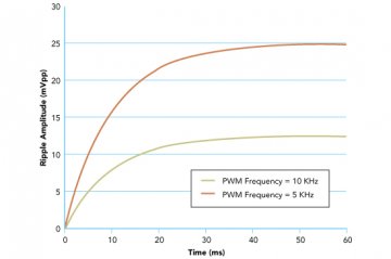
There are a couple of additional things to consider. Increasing the PWM frequency will also decrease the ripple, but the tradeoff is increased settling time. Figure 7 shows the cases for 10 kHz and 5 kHz
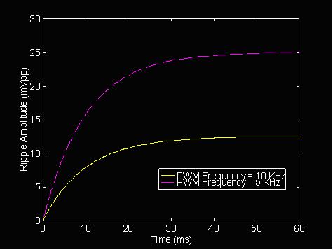
Figure 7: Voltage Ripple at the PWM DAC when PWM Frequency Changes. Where VOH = 5V, C = 1μF, R = 10 kΩ, Duty Cycle = 50 %, PWM Frequency = 10 kHz and 5 kHz
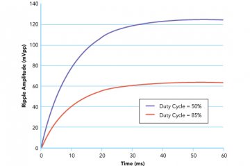
The worst-case ripple occurs at a 50% duty cycle. The ripple will decrease as the duty cycle moves closer to 0% or 100%. Figure 8 shows the peak-to-peak magnitude of ripples on the PWM DAC output. The ripple decreases almost two times as the duty cycle changes from 50 % to 85 %.
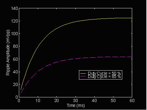
Figure 8: Voltage Ripple at the PWM DAC when PWM Duty Cycle Changes. VOH = 5V, C = 10 μF, R = 1 kΩ, PWM Frequency = 1 kHz, Duty Cycle = 50 % (Solid Curve) and 85 % (Dotted Curve)
PWM DACs and Power Consumption
Many electronic products today are portable or handheld devices. These devices are battery powered, and many have strict constraints with regard to power consumption. Therefore, it is a good idea to minimize the PWM DAC’s power consumption. The current consumed in the PWM solution is simple to approximate, using the following equation:
 (8)
(8)
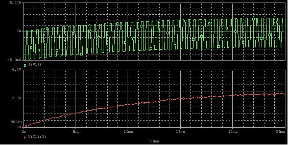
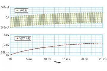
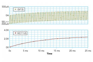
Figure 9: Current and Voltage Plots of PWM DAC with R =1000 Ω, C = 10μF, Duty Cycle = 50 %, VOH = 5V
Figure 9 shows the current and voltage plots. As sown in the plot, the PWM DAC with a lower resistor draws a significant amount of current (in the range of a few mA). This high level of current consumption is unacceptable for many battery-powered applications. Current can be decreased by increasing the resistor value.
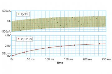
In Figure 10, the resistor value has been increased by a factor of ten, which has likewise decreased the current consumption by a factor of ten.
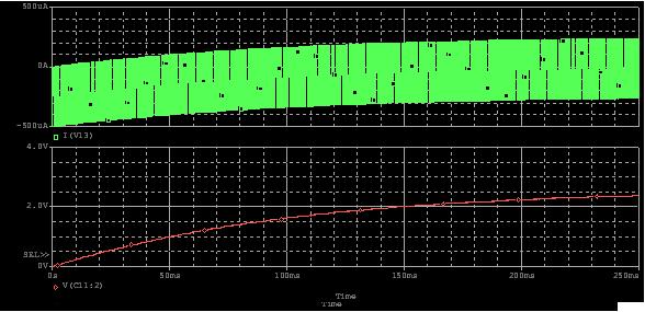
Figure 10: Current and Voltage Plots of PWM DAC with R =10,000 Ω, C = 10μF, Duty Cycle = 50 %, VOH = 5V
As the resistor limits the current available to charge/discharge the capacitor, decreasing the amount of current available (increasing resistance) to the circuit will increase the settling time.
Another factor to consider is the filter’s pole. As the resistor value increases, the 3 dB frequency decreases by the same magnitude. This can be compensated for by reducing the capacitor value by the same magnitude, which offsets the increased settling time and maintains the original pole of the filter. Figure 11 demonstrates this. Note that, as the capacitor value reduces, the circuit becomes more susceptible to loading. This is another important design consideration.
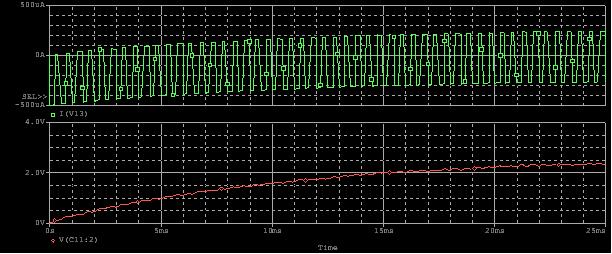
Figure 11: Current and Voltage Plots of PWM DAC with R =10,000 Ω, C = 1μF, Duty Cycle = 50 %, VOH = 5Vircuit

 浙公网安备 33010602011771号