

(原創) 如何實現Real Time的Sobel Edge Detector? (SOC) (Verilog) (Image Processing) (DE2-70) (TRDB-D5M) (TRDB-LTM)
 本文使用Verilog在DE2-70實現Sobel Edge Detector,並深入探討Line Buffer在Video Processing上的應用。
Abstract
本文使用Verilog在DE2-70實現Sobel Edge Detector,並深入探討Line Buffer在Video Processing上的應用。
Introduction
使用環境:Quartus II 8.0 + DE2-70 (Cyclone II EP2C70F896C6N) + TRDB-D5M + TRDB-LTM
Sobel Edge Detector是常用的Edge Detection演算法,在(原創) 如何實現Sobel Edge Detector? (Image Processing) (C/C++) (C++/CLI) (C)中,我曾經使用C與C++/CLI以軟體的方式實現, 在本文,我會用Verilog以硬體的方式在FPGA上實現。
用Verilog做影像處理所遇到的難題
用C做影像處理,大抵都是先將每個pixel的RGB放在二維的array中,由於C本身語言的特性,或許你會改用一維array,但觀念上其實仍是二維array。不過不管怎樣,總是有個記憶體位址能實際掌握每個pixel的RGB資訊。
但用Verilog做影像處理,由於是real time,SDRAM只是frame buffer,可以看成是一個FIFO,影像不斷地從CMOS進來,經過SDRAM之後,不斷地從VGA出去,我們並無法使用記憶體位址的概念去存取每個pixel的RGB資訊,也無法建立一個二維array來存取,這是用Verilog做影像處理所面臨最大的挑戰。
Sobel Edge Detector
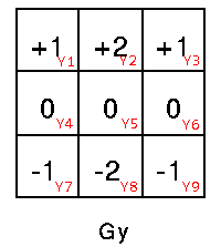
詳細的Sobel演算法流程,我就不再多談,請參考Sobel Edge Detector。下圖的Gx與Gy是Sobel edge detector在X方向與Y方向的kernel,將與P5這個pixel做convolution。
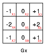
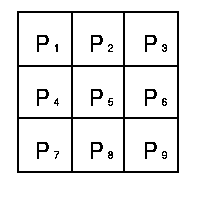
雖然是對P5運算,卻必須同時知道P1、P2、P3、P4、P6、P7、P8、P9的資訊,這在C不是問題,因為都在array內,只要改變一下array的index就可得到,但在Verilog卻做不到。
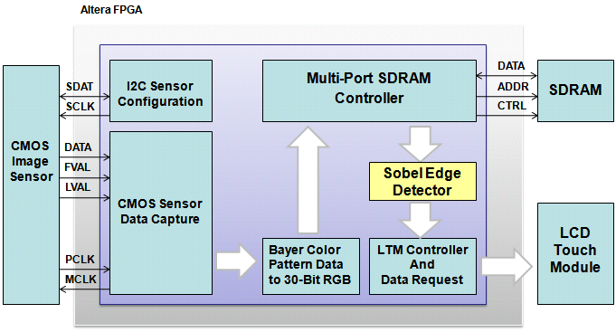
系統架構圖
使用Verilog實現Sobel Edge Detector
Sobel.v / Verilog
2 (C) OOMusou 2008 http://oomusou.cnblogs.com
3
4 Filename : Sobel.v
5 Compiler : Quartus II 8.0
6 Description : Demo how to implement Sobel Edge Detector on DE2-70
7 Release : 09/27/2008 1.0
8 */
9
10 module Sobel (
11 input iCLK,
12 input iRST_N,
13 input [7:0] iTHRESHOLD,
14 input iDVAL,
15 input [9:0] iDATA,
16 output reg oDVAL,
17 output reg [9:0] oDATA
18 );
19
20 // mask x
21 parameter X1 = 8'hff, X2 = 8'h00, X3 = 8'h01;
22 parameter X4 = 8'hfe, X5 = 8'h00, X6 = 8'h02;
23 parameter X7 = 8'hff, X8 = 8'h00, X9 = 8'h01;
24
25 // mask y
26 parameter Y1 = 8'h01, Y2 = 8'h02, Y3 = 8'h01;
27 parameter Y4 = 8'h00, Y5 = 8'h00, Y6 = 8'h00;
28 parameter Y7 = 8'hff, Y8 = 8'hfe, Y9 = 8'hff;
29
30 wire [7:0] Line0;
31 wire [7:0] Line1;
32 wire [7:0] Line2;
33
34 wire [17:0] Mac_x0;
35 wire [17:0] Mac_x1;
36 wire [17:0] Mac_x2;
37
38 wire [17:0] Mac_y0;
39 wire [17:0] Mac_y1;
40 wire [17:0] Mac_y2;
41
42 wire [19:0] Pa_x;
43 wire [19:0] Pa_y;
44
45 wire [15:0] Abs_mag;
46
47 LineBuffer_3 b0 (
48 .clken(iDVAL),
49 .clock(iCLK),
50 .shiftin(iDATA[9:2]),
51 .taps0x(Line0),
52 .taps1x(Line1),
53 .taps2x(Line2)
54 );
55
56 // X
57 MAC_3 x0 (
58 .aclr0(!iRST_N),
59 .clock0(iCLK),
60 .dataa_0(Line0),
61 .datab_0(X9),
62 .datab_1(X8),
63 .datab_2(X7),
64 .result(Mac_x0)
65 );
66
67 MAC_3 x1 (
68 .aclr0(!iRST_N),
69 .clock0(iCLK),
70 .dataa_0(Line1),
71 .datab_0(X6),
72 .datab_1(X5),
73 .datab_2(X4),
74 .result(Mac_x1)
75 );
76
77 MAC_3 x2 (
78 .aclr0(!iRST_N),
79 .clock0(iCLK),
80 .dataa_0(Line2),
81 .datab_0(X3),
82 .datab_1(X2),
83 .datab_2(X1),
84 .result(Mac_x2)
85 );
86
87 // Y
88 MAC_3 y0 (
89 .aclr0(!iRST_N),
90 .clock0(iCLK),
91 .dataa_0(Line0),
92 .datab_0(Y9),
93 .datab_1(Y8),
94 .datab_2(Y7),
95 .result(Mac_y0)
96 );
97
98 MAC_3 y1 (
99 .aclr0(!iRST_N),
100 .clock0(iCLK),
101 .dataa_0(Line1),
102 .datab_0(Y6),
103 .datab_1(Y5),
104 .datab_2(Y4),
105 .result(Mac_y1)
106 );
107
108 MAC_3 y2 (
109 .aclr0(!iRST_N),
110 .clock0(iCLK),
111 .dataa_0(Line2),
112 .datab_0(Y3),
113 .datab_1(Y2),
114 .datab_2(Y1),
115 .result(Mac_y2)
116 );
117
118 PA_3 pa0 (
119 .clock(iCLK),
120 .data0x(Mac_x0),
121 .data1x(Mac_x1),
122 .data2x(Mac_x2),
123 .result(Pa_x)
124 );
125
126 PA_3 pa1 (
127 .clock(iCLK),
128 .data0x(Mac_y0),
129 .data1x(Mac_y1),
130 .data2x(Mac_y2),
131 .result(Pa_y)
132 );
133
134 SQRT sqrt0 (
135 .clk(iCLK),
136 .radical(Pa_x * Pa_x + Pa_y * Pa_y),
137 .q(Abs_mag)
138 );
139
140 always@(posedge iCLK, negedge iRST_N) begin
141 if (!iRST_N)
142 oDVAL <= 0;
143 else begin
144 oDVAL <= iDVAL;
145
146 if (iDVAL)
147 oDATA <= (Abs_mag > iTHRESHOLD) ? 0 : 1023;
148 else
149 oDATA <= 0;
150 end
151 end
152
153 endmodule
19行
parameter X1 = 8'hff, X2 = 8'h00, X3 = 8'h01;
parameter X4 = 8'hfe, X5 = 8'h00, X6 = 8'h02;
parameter X7 = 8'hff, X8 = 8'h00, X9 = 8'h01;
// mask y
parameter Y1 = 8'h01, Y2 = 8'h02, Y3 = 8'h01;
parameter Y4 = 8'h00, Y5 = 8'h00, Y6 = 8'h00;
parameter Y7 = 8'hff, Y8 = 8'hfe, Y9 = 8'hff;
定義Sobel的Gx與Gy兩個kernel,X1因為是-1,所以用的是2's complement。
48行
.clken(iDVAL),
.clock(iCLK),
.shiftin(iDATA[9:2]),
.taps0x(Line0),
.taps1x(Line1),
.taps2x(Line2)
);
本文最關鍵的地方就在這個Line Buffer,也是最難理解的地方,為了講解方便,先假設一個frame只有9個pixel,欲搭配Gx做運算,如下圖所示:
根據Sobel edge detector演算法:
X1 ~ X9沒問題,都已經在parameter上了,但 P1 ~ P9的取得就是大問題, 他是P1、P2、P3....P9依序的傳入,沒有C的位址概念,也沒有2維array概念,為此我特別設計了3條line buffer做以上的運算。
3條line buffer使用Megafunction的altshift_tab達成,與Gx乘加的部分由Megafunction的altmult_add與parallel_add完成。
為了加強了解,我特別設計了只有3條line buffer,每條line buffer只有3個pixel的小程式來仿真:

我們可以發現,在最後一個pixel:9輸入後,下一個clock得到的是pixel 1、4、7,在下一個clock是2、5、8、最後一個clock是9、6、3,也就是Line0依次得到9、8、7,Line1得到6、5、4,Line3得到3、2、1,所以Line0必須與X9、X8、X7做乘加,其餘同理,所以在58行
MAC_3 x0 (
.aclr0(!iRST_N),
.clock0(iCLK),
.dataa_0(Line0),
.datab_0(X9),
.datab_1(X8),
.datab_2(X7),
.result(Mac_x0)
);
Mac_3是Megafunction的altmult_add,其餘的x1、x2與y0、y1、y2同理。
119行
.clock(iCLK),
.data0x(Mac_x0),
.data1x(Mac_x1),
.data2x(Mac_x2),
.result(Pa_x)
);
使用Megafunction的parallel_add做加總,pa1同理。
135行
.clk(iCLK),
.radical(Pa_x * Pa_x + Pa_y * Pa_y),
.q(Abs_mag)
);
根據Sobel演算法,要平方相加再開根號,其實只是為了取正值而已,也可以簡單的用 |Pa_x| + |Pa_y|計算。
46行
判斷threshold值。
在DE2-70實現Sobel Edge Detector
我是以DE2-70 CD中的DE2_70_D5M_LTM為藍本修改而成,這是一個以DE2-70 + 500萬像素CMOS:TRDB-D5M + 4.3寸 800x400 LTM為平台的範例。
DE2_70.v / Verilog
2 (C) OOMusou 2008 http://oomusou.cnblogs.com
3
4 Filename : DE2_70.v
5 Compiler : Quartus II 8.0
6 Description : Demo how to implement Sobel Edge Detector on DE2-70
7 Release : 08/25/2008 1.0
8 */
9
10 module DE2_70 (
11 //////////////////////// Clock Input ////////////////////////
12 input iCLK_28, // 28.63636 MHz
13 input iCLK_50, // 50 MHz
14 input iCLK_50_2, // 50 MHz
15 input iCLK_50_3, // 50 MHz
16 input iCLK_50_4, // 50 MHz
17 input iEXT_CLOCK, // External Clock
18 //////////////////////// Push Button ////////////////////////
19 input [3:0] iKEY, // Pushbutton[3:0]
20 //////////////////////// DPDT Switch ////////////////////////
21 input [17:0] iSW, // Toggle Switch[17:0]
22 //////////////////////// 7-SEG Dispaly ////////////////////////
23 output [6:0] oHEX0_D, // Seven Segment Digit 0
24 output oHEX0_DP, // Seven Segment Digit 0 decimal point
25 output [6:0] oHEX1_D, // Seven Segment Digit 1
26 output oHEX1_DP, // Seven Segment Digit 1 decimal point
27 output [6:0] oHEX2_D, // Seven Segment Digit 2
28 output oHEX2_DP, // Seven Segment Digit 2 decimal point
29 output [6:0] oHEX3_D, // Seven Segment Digit 3
30 output oHEX3_DP, // Seven Segment Digit 3 decimal point
31 output [6:0] oHEX4_D, // Seven Segment Digit 4
32 output oHEX4_DP, // Seven Segment Digit 4 decimal point
33 output [6:0] oHEX5_D, // Seven Segment Digit 5
34 output oHEX5_DP, // Seven Segment Digit 5 decimal point
35 output [6:0] oHEX6_D, // Seven Segment Digit 6
36 output oHEX6_DP, // Seven Segment Digit 6 decimal point
37 output [6:0] oHEX7_D, // Seven Segment Digit 7
38 output oHEX7_DP, // Seven Segment Digit 7 decimal point
39 //////////////////////////// LED ////////////////////////////
40 output [8:0] oLEDG, // LED Green[8:0]
41 output [17:0] oLEDR, // LED Red[17:0]
42 //////////////////////////// UART ////////////////////////////
43 output oUART_TXD, // UART Transmitter
44 input iUART_RXD, // UART Receiver
45 output oUART_CTS, // UART Clear To Send
46 input iUART_RTS, // UART Requst To Send
47 //////////////////////////// IRDA ////////////////////////////
48 output oIRDA_TXD, // IRDA Transmitter
49 input iIRDA_RXD, // IRDA Receiver
50 /////////////////////// SDRAM Interface ////////////////////////
51 inout [31:0] DRAM_DQ, // SDRAM Data bus 32 Bits
52 output [12:0] oDRAM0_A, // SDRAM0 Address bus 13 Bits
53 output [12:0] oDRAM1_A, // SDRAM1 Address bus 13 Bits
54 output oDRAM0_LDQM0, // SDRAM0 Low-byte Data Mask
55 output oDRAM1_LDQM0, // SDRAM1 Low-byte Data Mask
56 output oDRAM0_UDQM1, // SDRAM0 High-byte Data Mask
57 output oDRAM1_UDQM1, // SDRAM1 High-byte Data Mask
58 output oDRAM0_WE_N, // SDRAM0 Write Enable
59 output oDRAM1_WE_N, // SDRAM1 Write Enable
60 output oDRAM0_CAS_N, // SDRAM0 Column Address Strobe
61 output oDRAM1_CAS_N, // SDRAM1 Column Address Strobe
62 output oDRAM0_RAS_N, // SDRAM0 Row Address Strobe
63 output oDRAM1_RAS_N, // SDRAM1 Row Address Strobe
64 output oDRAM0_CS_N, // SDRAM0 Chip Select
65 output oDRAM1_CS_N, // SDRAM1 Chip Select
66 output [1:0] oDRAM0_BA, // SDRAM0 Bank Address
67 output [1:0] oDRAM1_BA, // SDRAM1 Bank Address
68 output oDRAM0_CLK, // SDRAM0 Clock
69 output oDRAM1_CLK, // SDRAM1 Clock
70 output oDRAM0_CKE, // SDRAM0 Clock Enable
71 output oDRAM1_CKE, // SDRAM1 Clock Enable
72 //////////////////////// Flash Interface ////////////////////////
73 inout [14:0] FLASH_DQ, // FLASH Data bus 15 Bits (0 to 14)
74 inout FLASH_DQ15_AM1, // FLASH Data bus Bit 15 or Address A-1
75 output [21:0] oFLASH_A, // FLASH Address bus 26 Bits
76 output oFLASH_WE_N, // FLASH Write Enable
77 output oFLASH_RST_N, // FLASH Reset
78 output oFLASH_WP_N, // FLASH Write Protect /Programming Acceleration
79 input iFLASH_RY_N, // FLASH Ready/Busy output
80 output oFLASH_BYTE_N, // FLASH Byte/Word Mode Configuration
81 output oFLASH_OE_N, // FLASH Output Enable
82 output oFLASH_CE_N, // FLASH Chip Enable
83 //////////////////////// SRAM Interface ////////////////////////
84 inout [31:0] SRAM_DQ, // SRAM Data Bus 32 Bits
85 inout [3:0] SRAM_DPA, // SRAM Parity Data Bus
86 output [18:0] oSRAM_A, // SRAM Address bus 21 Bits
87 output oSRAM_ADSC_N, // SRAM Controller Address Status
88 output oSRAM_ADSP_N, // SRAM Processor Address Status
89 output oSRAM_ADV_N, // SRAM Burst Address Advance
90 output [3:0] oSRAM_BE_N, // SRAM Byte Write Enable
91 output oSRAM_CE1_N, // SRAM Chip Enable
92 output oSRAM_CE2, // SRAM Chip Enable
93 output oSRAM_CE3_N, // SRAM Chip Enable
94 output oSRAM_CLK, // SRAM Clock
95 output oSRAM_GW_N, // SRAM Global Write Enable
96 output oSRAM_OE_N, // SRAM Output Enable
97 output oSRAM_WE_N, // SRAM Write Enable
98 //////////////////// ISP1362 Interface ////////////////////////
99 inout [15:0] OTG_D, // ISP1362 Data bus 16 Bits
100 output [1:0] oOTG_A, // ISP1362 Address 2 Bits
101 output oOTG_CS_N, // ISP1362 Chip Select
102 output oOTG_OE_N, // ISP1362 Read
103 output oOTG_WE_N, // ISP1362 Write
104 output oOTG_RESET_N, // ISP1362 Reset
105 inout OTG_FSPEED, // USB Full Speed, 0 = Enable, Z = Disable
106 inout OTG_LSPEED, // USB Low Speed, 0 = Enable, Z = Disable
107 input iOTG_INT0, // ISP1362 Interrupt 0
108 input iOTG_INT1, // ISP1362 Interrupt 1
109 input iOTG_DREQ0, // ISP1362 DMA Request 0
110 input iOTG_DREQ1, // ISP1362 DMA Request 1
111 output oOTG_DACK0_N, // ISP1362 DMA Acknowledge 0
112 output oOTG_DACK1_N, // ISP1362 DMA Acknowledge 1
113 //////////////////// LCD Module 16X2 ////////////////////////////
114 inout [7:0] LCD_D, // LCD Data bus 8 bits
115 output oLCD_ON, // LCD Power ON/OFF
116 output oLCD_BLON, // LCD Back Light ON/OFF
117 output oLCD_RW, // LCD Read/Write Select, 0 = Write, 1 = Read
118 output oLCD_EN, // LCD Enable
119 output oLCD_RS, // LCD Command/Data Select, 0 = Command, 1 = Data
120 //////////////////// SD Card Interface ////////////////////////
121 inout SD_DAT, // SD Card Data
122 inout SD_DAT3, // SD Card Data 3
123 inout SD_CMD, // SD Card Command Signal
124 output oSD_CLK, // SD Card Clock
125 //////////////////////// I2C ////////////////////////////////
126 inout I2C_SDAT, // I2C Data
127 output oI2C_SCLK, // I2C Clock
128 //////////////////////// PS2 ////////////////////////////////
129 inout PS2_KBDAT, // PS2 Keyboard Data
130 inout PS2_KBCLK, // PS2 Keyboard Clock
131 inout PS2_MSDAT, // PS2 Mouse Data
132 inout PS2_MSCLK, // PS2 Mouse Clock
133 //////////////////////// VGA ////////////////////////////
134 output oVGA_CLOCK, // VGA Clock
135 output oVGA_HS, // VGA H_SYNC
136 output oVGA_VS, // VGA V_SYNC
137 output oVGA_BLANK_N, // VGA BLANK
138 output oVGA_SYNC_N, // VGA SYNC
139 output [9:0] oVGA_R, // VGA Red[9:0]
140 output [9:0] oVGA_G, // VGA Green[9:0]
141 output [9:0] oVGA_B, // VGA Blue[9:0]
142 //////////////// Ethernet Interface ////////////////////////////
143 inout [15:0] ENET_D, // DM9000A DATA bus 16Bits
144 output oENET_CMD, // DM9000A Command/Data Select, 0 = Command, 1 = Data
145 output oENET_CS_N, // DM9000A Chip Select
146 output oENET_IOW_N, // DM9000A Write
147 output oENET_IOR_N, // DM9000A Read
148 output oENET_RESET_N, // DM9000A Reset
149 input iENET_INT, // DM9000A Interrupt
150 output oENET_CLK, // DM9000A Clock 25 MHz
151 //////////////////// Audio CODEC ////////////////////////////
152 inout AUD_ADCLRCK, // Audio CODEC ADC LR Clock
153 input iAUD_ADCDAT, // Audio CODEC ADC Data
154 inout AUD_DACLRCK, // Audio CODEC DAC LR Clock
155 output oAUD_DACDAT, // Audio CODEC DAC Data
156 inout AUD_BCLK, // Audio CODEC Bit-Stream Clock
157 output oAUD_XCK, // Audio CODEC Chip Clock
158 //////////////////// TV Devoder ////////////////////////////
159 input iTD1_CLK27, // TV Decoder1 Line_Lock Output Clock
160 input [7:0] iTD1_D, // TV Decoder1 Data bus 8 bits
161 input iTD1_HS, // TV Decoder1 H_SYNC
162 input iTD1_VS, // TV Decoder1 V_SYNC
163 output oTD1_RESET_N, // TV Decoder1 Reset
164 input iTD2_CLK27, // TV Decoder2 Line_Lock Output Clock
165 input [7:0] iTD2_D, // TV Decoder2 Data bus 8 bits
166 input iTD2_HS, // TV Decoder2 H_SYNC
167 input iTD2_VS, // TV Decoder2 V_SYNC
168 output oTD2_RESET_N, // TV Decoder2 Reset
169 //////////////////////// GPIO ////////////////////////////////
170 inout [31:0] GPIO_0, // GPIO Connection 0 I/O
171 input GPIO_CLKIN_N0, // GPIO Connection 0 Clock Input 0
172 input GPIO_CLKIN_P0, // GPIO Connection 0 Clock Input 1
173 inout GPIO_CLKOUT_N0, // GPIO Connection 0 Clock Output 0
174 inout GPIO_CLKOUT_P0, // GPIO Connection 0 Clock Output 1
175 inout [31:0] GPIO_1, // GPIO Connection 1 I/O
176 input GPIO_CLKIN_N1, // GPIO Connection 1 Clock Input 0
177 input GPIO_CLKIN_P1, // GPIO Connection 1 Clock Input 1
178 inout GPIO_CLKOUT_N1, // GPIO Connection 1 Clock Output 0
179 inout GPIO_CLKOUT_P1 // GPIO Connection 1 Clock Output 1
180 );
181
182 wire [11:0] CCD_DATA;
183 wire CCD_SDAT;
184 wire CCD_SCLK;
185 wire CCD_FLASH;
186 wire CCD_FVAL;
187 wire CCD_LVAL;
188 wire CCD_PIXCLK;
189 wire CCD_MCLK; // CCD Master Clock
190
191 wire [15:0] Read_DATA1;
192 wire [15:0] Read_DATA2;
193 wire VGA_CTRL_CLK;
194 wire [11:0] mCCD_DATA;
195 wire mCCD_DVAL;
196 wire mCCD_DVAL_d;
197 wire [15:0] X_Cont;
198 wire [15:0] Y_Cont;
199 wire [9:0] X_ADDR;
200 wire [31:0] Frame_Cont;
201 wire DLY_RST_0;
202 wire DLY_RST_1;
203 wire DLY_RST_2;
204 wire Read;
205 reg [11:0] rCCD_DATA;
206 reg rCCD_LVAL;
207 reg rCCD_FVAL;
208 wire [11:0] sCCD_R;
209 wire [11:0] sCCD_G;
210 wire [11:0] sCCD_B;
211 wire sCCD_DVAL;
212 reg [1:0] rClk;
213 wire sdram_ctrl_clk;
214
215
216 // Touch panel signal
217 wire [7:0] ltm_r; // LTM Red Data 8 Bits
218 wire [7:0] ltm_g; // LTM Green Data 8 Bits
219 wire [7:0] ltm_b; // LTM Blue Data 8 Bits
220 wire ltm_nclk; // LTM Clcok
221 wire ltm_hd;
222 wire ltm_vd;
223 wire ltm_den;
224 wire adc_dclk;
225 wire adc_cs;
226 wire adc_penirq_n;
227 wire adc_busy;
228 wire adc_din;
229 wire adc_dout;
230 wire adc_ltm_sclk;
231 wire ltm_grst;
232 // LTM Config
233 wire ltm_sclk;
234 wire ltm_sda;
235 wire ltm_scen;
236 wire ltm_3wirebusy_n;
237
238 assign CCD_DATA[0] = GPIO_1[11];
239 assign CCD_DATA[1] = GPIO_1[10];
240 assign CCD_DATA[2] = GPIO_1[9];
241 assign CCD_DATA[3] = GPIO_1[8];
242 assign CCD_DATA[4] = GPIO_1[7];
243 assign CCD_DATA[5] = GPIO_1[6];
244 assign CCD_DATA[6] = GPIO_1[5];
245 assign CCD_DATA[7] = GPIO_1[4];
246 assign CCD_DATA[8] = GPIO_1[3];
247 assign CCD_DATA[9] = GPIO_1[2];
248 assign CCD_DATA[10] = GPIO_1[1];
249 assign CCD_DATA[11] = GPIO_1[0];
250 assign GPIO_CLKOUT_N1 = CCD_MCLK;
251 assign CCD_FVAL = GPIO_1[18];
252 assign CCD_LVAL = GPIO_1[17];
253 assign CCD_PIXCLK = GPIO_CLKIN_N1;
254 assign GPIO_1[15] = 1'b1; // tRIGGER
255 assign GPIO_1[14] = DLY_RST_1;
256
257 assign oLEDR = iSW;
258 assign oLEDG = Y_Cont;
259
260 assign oTD1_RESET_N = 1'b1;
261 assign oVGA_CLOCK = VGA_CTRL_CLK;
262
263 assign CCD_MCLK = rClk[0];
264
265 assign oUART_TXD = iUART_RXD;
266
267 assign adc_penirq_n = GPIO_CLKIN_N0;
268 assign adc_dout = GPIO_0[0];
269 assign adc_busy = GPIO_CLKIN_P0;
270 assign GPIO_0[1] = adc_din;
271 assign GPIO_0[2] = adc_ltm_sclk;
272 assign GPIO_0[3] = ltm_b[3];
273 assign GPIO_0[4] = ltm_b[2];
274 assign GPIO_0[5] = ltm_b[1];
275 assign GPIO_0[6] = ltm_b[0];
276 assign GPIO_0[7] =~ltm_nclk;
277 assign GPIO_0[8] =ltm_den;
278 assign GPIO_0[9] =ltm_hd;
279 assign GPIO_0[10] =ltm_vd;
280 assign GPIO_0[11] =ltm_b[4];
281 assign GPIO_0[12] =ltm_b[5];
282 assign GPIO_0[13] =ltm_b[6];
283 assign GPIO_CLKOUT_N0=ltm_b[7];
284 assign GPIO_0[14] =ltm_g[0];
285 assign GPIO_CLKOUT_P0=ltm_g[1];
286 assign GPIO_0[15] =ltm_g[2];
287 assign GPIO_0[16] =ltm_g[3];
288 assign GPIO_0[17] =ltm_g[4];
289 assign GPIO_0[18] =ltm_g[5];
290 assign GPIO_0[19] =ltm_g[6];
291 assign GPIO_0[20] =ltm_g[7];
292 assign GPIO_0[21] =ltm_r[0];
293 assign GPIO_0[22] =ltm_r[1];
294 assign GPIO_0[23] =ltm_r[2];
295 assign GPIO_0[24] =ltm_r[3];
296 assign GPIO_0[25] =ltm_r[4];
297 assign GPIO_0[26] =ltm_r[5];
298 assign GPIO_0[27] =ltm_r[6];
299 assign GPIO_0[28] =ltm_r[7];
300 assign GPIO_0[29] =ltm_grst;
301 assign GPIO_0[30] =ltm_scen;
302 assign GPIO_0[31] =ltm_sda;
303
304 assign ltm_grst = iKEY[0];
305 assign adc_ltm_sclk = ltm_sclk ;
306
307
308
309
310
311
312 always@(posedge iCLK_50)
313 rClk <= rClk+1;
314
315 always@(posedge CCD_PIXCLK) begin
316 rCCD_DATA <= CCD_DATA;
317 rCCD_LVAL <= CCD_LVAL;
318 rCCD_FVAL <= CCD_FVAL;
319 end
320
321 Reset_Delay reset0 (
322 .iCLK(iCLK_50),
323 .iRST(iKEY[0]),
324 .oRST_0(DLY_RST_0),
325 .oRST_1(DLY_RST_1),
326 .oRST_2(DLY_RST_2)
327 );
328
329 CCD_Capture capture0 (
330 .oDATA(mCCD_DATA),
331 .oDVAL(mCCD_DVAL),
332 .oX_Cont(X_Cont),
333 .oY_Cont(Y_Cont),
334 .oFrame_Cont(Frame_Cont),
335 .iDATA(rCCD_DATA),
336 .iFVAL(rCCD_FVAL),
337 .iLVAL(rCCD_LVAL),
338 .iSTART(!iKEY[3]),
339 .iEND(!iKEY[2]),
340 .iCLK(CCD_PIXCLK),
341 .iRST(DLY_RST_2)
342 );
343
344 RAW2RGB raw0 (
345 .iCLK(CCD_PIXCLK),
346 .iRST_n(DLY_RST_1),
347 .iData(mCCD_DATA),
348 .iDval(mCCD_DVAL),
349 .oRed(sCCD_R),
350 .oGreen(sCCD_G),
351 .oBlue(sCCD_B),
352 .oDval(sCCD_DVAL),
353 .iMIRROR(iSW[17]),
354 .iX_Cont(X_Cont),
355 .iY_Cont(Y_Cont)
356 );
357
358 SEG7_LUT_8 seg0 (
359 .oSEG0(oHEX0_D),
360 .oSEG1(oHEX1_D),
361 .oSEG2(oHEX2_D),
362 .oSEG3(oHEX3_D),
363 .oSEG4(oHEX4_D),
364 .oSEG5(oHEX5_D),
365 .oSEG6(oHEX6_D),
366 .oSEG7(oHEX7_D),
367 .iDIG(Frame_Cont[31:0])
368 );
369
370 vga_pll vga_pll0 (
371 .inclk0(iCLK_50_2),
372 .c0(ltm_nclk)
373 );
374
375 sdram_pll sdram_pll0 (
376 .inclk0(iCLK_50_3),
377 .c0(sdram_ctrl_clk),
378 .c1(oDRAM0_CLK),
379 .c2(oDRAM1_CLK)
380 );
381
382 Sdram_Control_4Port sdram0 (
383 // HOST Side
384 .REF_CLK(iCLK_50),
385 .RESET_N(1'b1),
386 .CLK(sdram_ctrl_clk),
387 // FIFO Write Side 1
388 .WR1_DATA({sCCD_G[11:7], sCCD_B[11:2]}),
389 .WR1(sCCD_DVAL),
390 .WR1_ADDR(0),
391 .WR1_MAX_ADDR(800*480),
392 .WR1_LENGTH(9'h100),
393 .WR1_LOAD(!DLY_RST_0),
394 .WR1_CLK(CCD_PIXCLK),
395 // FIFO Read Side 1
396 .RD1_DATA(Read_DATA1),
397 .RD1(wDAL_sobel),
398 .RD1_ADDR(0),
399 .RD1_MAX_ADDR(800*480),
400 .RD1_LENGTH(9'h100),
401 .RD1_LOAD(!DLY_RST_0),
402 .RD1_CLK(~ltm_nclk),
403 // SDRAM Side
404 .SA(oDRAM0_A[11:0]),
405 .BA(oDRAM0_BA),
406 .CS_N(oDRAM0_CS_N),
407 .CKE(oDRAM0_CKE),
408 .RAS_N(oDRAM0_RAS_N),
409 .CAS_N(oDRAM0_CAS_N),
410 .WE_N(oDRAM0_WE_N),
411 .DQ(DRAM_DQ[15:0]),
412 .DQM({oDRAM0_UDQM1,oDRAM0_LDQM0})
413 );
414
415 Sdram_Control_4Port sdram1 (
416 // HOST Side
417 .REF_CLK(iCLK_50),
418 .RESET_N(1'b1),
419 .CLK(sdram_ctrl_clk),
420 // FIFO Write Side 1
421 .WR1_DATA({sCCD_G[6:2], sCCD_R[11:2]}),
422 .WR1(sCCD_DVAL),
423 .WR1_ADDR(0),
424 .WR1_MAX_ADDR(800*480),
425 .WR1_LENGTH(9'h100),
426 .WR1_LOAD(!DLY_RST_0),
427 .WR1_CLK(CCD_PIXCLK),
428 // FIFO Read Side 1
429 .RD1_DATA(Read_DATA2),
430 .RD1(wDAL_sobel),
431 .RD1_ADDR(0),
432 .RD1_MAX_ADDR(800*480),
433 .RD1_LENGTH(9'h100),
434 .RD1_LOAD(!DLY_RST_0),
435 .RD1_CLK(~ltm_nclk),
436 // SDRAM Side
437 .SA(oDRAM1_A[11:0]),
438 .BA(oDRAM1_BA),
439 .CS_N(oDRAM1_CS_N),
440 .CKE(oDRAM1_CKE),
441 .RAS_N(oDRAM1_RAS_N),
442 .CAS_N(oDRAM1_CAS_N),
443 .WE_N(oDRAM1_WE_N),
444 .DQ(DRAM_DQ[31:16]),
445 .DQM({oDRAM1_UDQM1,oDRAM1_LDQM0})
446 );
447
448 I2C_CCD_Config i2c_ccd_config0 (
449 // Host Side
450 .iCLK(iCLK_50),
451 .iRST_N(DLY_RST_1),
452 .iEXPOSURE_ADJ(iKEY[1]),
453 .iEXPOSURE_DEC_p(iSW[0]),
454 .iMIRROR_SW(iSW[17]),
455 // I2C Side
456 .I2C_SCLK(GPIO_1[20]),
457 .I2C_SDAT(GPIO_1[19])
458 );
459
460 touch_tcon vga0 (
461 .iCLK(ltm_nclk),
462 .iRST_n(DLY_RST_2),
463 // sdram side
464 .iREAD_DATA1({wDISP_G[9:5], wDISP_B}),
465 .iREAD_DATA2({wDISP_G[4:0], wISP_R}),
466 .oREAD_SDRAM_EN(Read),
467 // lcd side
468 .oLCD_R(ltm_r),
469 .oLCD_G(ltm_g),
470 .oLCD_B(ltm_b),
471 .oHD(ltm_hd),
472 .oVD(ltm_vd),
473 .oDEN(ltm_den)
474 );
475
476 lcd_3wire_config lcd_config0 (
477 // Host Side
478 .iCLK(iCLK_50),
479 .iRST_n(DLY_RST_0),
480 // 3 wire Side
481 .o3WIRE_SCLK(ltm_sclk),
482 .io3WIRE_SDAT(ltm_sda),
483 .o3WIRE_SCEN(ltm_scen),
484 .o3WIRE_BUSY_n(ltm_3wirebusy_n)
485 );
486
487 // sobel ----------------------------------------------------
488 // RGB
489 wire [9:0] wVGA_R = Read_DATA2[9:0];
490 wire [9:0] wVGA_G = {Read_DATA1[14:10],Read_DATA2[14:10]};
491 wire [9:0] wVGA_B = Read_DATA1[9:0];
492
493 // sobel
494 wire wDVAL_sobel;
495 wire [9:0] wSobel;
496
497 Sobel sobel0 (
498 .iCLK(ltm_nclk),
499 .iRST_N(DLY_RST_2),
500 .iTHRESHOLD(iSW[9:2]),
501 .iDVAL(Read),
502 .iDATA(wVGA_G), // gray
503 .oDVAL(wDAL_sobel),
504 .oDATA(wSobel)
505 );
506
507 // gray
508 wire [9:0] wGray_R = wVGA_G;
509 wire [9:0] wGray_G = wVGA_G;
510 wire [9:0] wGray_B = wVGA_G;
511
512 // to display
513 wire [9:0] wDISP_R = iSW[15] ? wGray_R : // Gray
514 iSW[14] ? wSobel : // Sobel
515 wVGA_R; // Color
516 wire [9:0] wDISP_G = iSW[15] ? wGray_G : // Gray
517 iSW[14] ? wSobel : // Sobel
518 wVGA_G; // Color
519 wire [9:0] wDISP_B = iSW[15] ? wGray_B : // Gray
520 iSW[14] ? wSobel : // Sobel
521 wVGA_B; // Color
522
523 endmodule
497行
.iCLK(ltm_nclk),
.iRST_N(DLY_RST_2),
.iTHRESHOLD(iSW[9:2]),
.iDVAL(Read),
.iDATA(wVGA_G), // gray
.oDVAL(wDAL_sobel),
.oDATA(wSobel)
);
引用剛剛所建立的Sobel.v module,為什麼iDATA()傳入的是mVGA_G呢?因為Sobel edge detector處理的是灰階影像,在(原創) 如何Real Time產生灰階影像? (SOC) (DE2) (TRDB-DC2)曾經談到使用G來代表灰階影像的理由。而SW[9:2]則可動態的調整threshold值。
512行
wire [9:0] wDISP_R = iSW[15] ? wGray_R : // Gray
iSW[14] ? wSobel : // Sobel
wVGA_R; // Color
wire [9:0] wDISP_G = iSW[15] ? wGray_G : // Gray
iSW[14] ? wSobel : // Sobel
wVGA_G; // Color
wire [9:0] wDISP_B = iSW[15] ? wGray_B : // Gray
iSW[14] ? wSobel : // Sobel
wVGA_B; // Color
加上了SW控制,可切換顯示彩色、灰階與經過Sobel取過edge的影像。
操作方式
KEY[0]:reset
KEY[1]:調整曝光值
KEY[2]:capture
KEY[3]:free run
SW[0]:on:減少曝光值模式,off : 增加曝光值模式
SW[2] ~ SW[9]:調整threshold
SW[15]:on:灰階模式,off:彩色模式
SW[15] off + SW[14] on:Sobel edge模式
SW[17]:on:啟動mirror,off:不啟動mirror
建議最佳Sobel edge模式:SW[5]、SW[6]、SW[14]、SW[17]為on,其他SW為off。
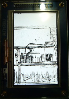
執行結果
依次為:彩色模式、灰階模式、Sobel edge模式
完整程式碼下載
DE2_70_D5M_LTM_sobel.7z
Altshift_tabs_lab0.7z (altshift_tabs仿真小程式)
Conclusion
本文的重點在於學會使用altshift_tab做line buffer,這招學會後,就可以運用在很多電腦視覺的演算法上。若要將這個方法運用在其他平台,如DE2的DE2_CCD範例上,別忘了要將line buffer的長度改為640,因為VGA是640 * 480,而不是本範例的800。
See Also
(原創) 如何實現Sobel Edge Detector? (Image Processing) (C/C++) (C++/CLI) (C)
(原創) 如何Real Time產生灰階影像? (SOC) (DE2) (TRDB-DC2)
(原創) 如何Real Time產生灰階影像? (SOC) (DE2-70) (TRDB-D5M)
(原創) 如何實現Real Time的Sobel Edge Detector? (SOC) (Verilog) (Image Processing) (DE2) (TRDB-DC2)
(原創) 如何實現Real Time對Binary Image做Dilation? (SOC) (Verilog) (Image Processing) (DE2-70) (TRDB-D5M) (TRDB-LTM)
(原創) 如何設計乘加電路? (SOC) (Verilog) (MegaCore)
(原創) 如何將DE2_70_TV範例加上Sobel Edge Detector? (SOC) (Verilog) (Image Processing) (DE2-70)

 浙公网安备 33010602011771号