
(原創) 深入探討Altera的Checksum Master範例 (SOC) (SOPC Builder) (Nios II) (DE2)
Abstract
checksum master是Quartus II Handbook Vol.4中示範Nios II與Avalon Bus應用的範例,是一個學習Nios II軟硬體設計很好的範本。
Introduction
使用環境:Quartus II 7.2 SP3 + Nios II EDS 7.2 SP3 + DE2(Cyclone II EP2C35F627C6)
本文無法取代Quartus II Handbook Vol.4 Ch.9介紹SOPC Builder使用部分,只將重心放在探討其source code以彌補手冊之不足,所以請先閱讀Quartus II Handbook Vol.4 Ch.9 Developing Components for SOPC Builder。
在(原創) 如何在DE2執行Checksum Master範例? (IC Design) (DE2) (Quartus II) (Nios II) (SOPC Builder)中,我曾經深入討論如何在DE2執行這個範例, 不過我當時並未深入去研究其code,也沒研究其演算法,只關注在slave interface部分,以及如何在DE2跑起來。最近花了時間仔細的看了一次,發現這真是個好範例,不虧是Quartus II Handbook Vol. 4中,唯一一個完整且具代表性的範例。
Checksum Master範例的特點
1.同時示範了master interface與slave interface,而前一代的PWM範例只示範了slave interface。
2.搭配Quartus II 7.1大改的SOPC Builder介面、新的程式寫法與更好的naming convention。
3.演算法部分很簡單,並沒有牽涉到什麼專業部分。
4.可從中學習到軟硬體設計的方法。
Checksum Master的演算法
首先先來看看CheckSum Master演算法的流程:
test_checksum.c / C
2 (C) OOMusou 2008 http://oomusou.cnblogs.com
3
4 Filename : test_checksum.c
5 Compiler : Nios II EDS 7.2 SP3
6 Description : Demo how to use checksum master component
7 Release : 07/29/2008 1.0
8 */
9 #include <stdio.h>
10 #include <stdlib.h>
11 #include "altera_avalon_checksum_regs.h"
12 #include "system.h"
13 #include <alt_types.h>
14
15 int len; // how many 8 bit 0xf0 will write to memory
16
17 /* Simple function that sets all contents of a buffer to the specified value. */
18 // buf8 : pointer for 8 bit int buffer
19 // offset : offset to buf8
20 // val : 0xf0 to write to memory
21 int set_buf_val(alt_u8* buf8, int offset, alt_u8 val) {
22 int ret_code = 0; // return code for success(0) or failure(-1)
23
24 /* Ok
 one byte at a time is not efficientC'est La Vie! */
25 while(offset>=0) {
26 *(buf8 + offset) = val; // write 0xf0 to memory
27 if (*(buf8 + offset) != val) // check whether write success
28 ret_code = -1;
29
30 offset--;
31 }
32
33 return ret_code;
34 }
35
36 /* This program points the checksum component at a small buffer and
37 * computes the checksum by hardware. */
38 void compute_by_hw() {
39 /* Setup the checksum component. */
40 /* IORD and IOWR macros setup in alter_avalon_checksum_regs.h and io.h */
41 int status; // computing status : busy or done?
42 int result; // result for checksum
43
44 /* Store the address (must be 32-bit word aligned address). */
45 printf("Writing to address register. \n");
46 IOWR_ALTERA_AVALON_CHECKSUM_ADDR(ALTERA_AVALON_CHECKSUM_INST_BASE, ONCHIP_RAM_BASE);
47
48 /* Store the length in bytes (up to a 16-bit value). */
49 printf("Writing to length register. \n");
50 IOWR_ALTERA_AVALON_CHECKSUM_LENGTH(ALTERA_AVALON_CHECKSUM_INST_BASE, len);
51
52 /* Tell it to "go". */
53 printf("Writing to go bit in control register. \n");
54 IOWR_ALTERA_AVALON_CHECKSUM_CTRL(ALTERA_AVALON_CHECKSUM_INST_BASE+ALTERA_AVALON_CHECKSUM_CTRL_GO_OFST, ALTERA_AVALON_CHECKSUM_CTRL_GO_MSK);
55
56 /* Polling loop waiting for the component to be done. */
57 status = IORD_ALTERA_AVALON_CHECKSUM_STATUS(ALTERA_AVALON_CHECKSUM_INST_BASE);
58 printf("Polling for DONE bit in status register. . . \n");
59 while (!(status & ALTERA_AVALON_CHECKSUM_STATUS_DONE_MSK))
60 status = IORD_ALTERA_AVALON_CHECKSUM_STATUS(ALTERA_AVALON_CHECKSUM_INST_BASE);
61
62 printf( "Done bit asserted, exiting polling loop. \n");
63
64 result = IORD_ALTERA_AVALON_CHECKSUM_RESULT(ALTERA_AVALON_CHECKSUM_INST_BASE);
65 printf( "Done
Result = 0x%x.\n", result);66 }
67
68 /* This program points the checksum component at a small buffer and
69 * computes the checksum by software. */
70 void compute_by_sw() {
71 alt_u32 *buf32 = (alt_u32*)ONCHIP_RAM_BASE; // pointer for 32 bit int buffer
72 alt_u32 sum_1; // sum_1 = *buf32[31:16] + *buf32[15:0]
73 alt_u32 sum_reg = 0;// sum of *buf32
74 alt_u32 sum_2; // sum_2 = sum_reg[31:16] + sum_reg[15:0]
75 alt_u32 sum_3; // sum_3 = sum_2[31:16] + sum_2[31:16]
76 int cnt = len * 8 / 32; // times to sum
77 int result; // one's complement for sum_3
78
79 while(cnt--) {
80 // verilog : assign sum_1 = data_in_reg[31:16] + data_in_reg[15:0];
81 sum_1 = (*buf32 & (0x0000ffff)) + ((*buf32 >> 16) & (0x0000ffff));
82
83 // verilog : assign next_sum_reg = sum_1 + sum_reg;
84 sum_reg += sum_1;
85 buf32++; // next 32 bit int buffer
86 }
87
88 // verilog : assign sum_2 = sum_reg[31:16] + sum_reg[15:0];
89 sum_2 = (sum_reg & (0x0000ffff)) + ((sum_reg >> 16) & (0x0000ffff));
90
91 // verilog : assign sum_3 = sum_2[31:16] + sum_2[15:0];
92 sum_3 = (sum_2 & (0x0000ffff)) + ((sum_2 >> 16) & (0x0000ffff));
93
94 // one's complement for sum_3
95 // verilog : assign result = {~(sum_3[15:0])};
96 result = (~(sum_3 & (0x0000ffff))) & (0x0000ffff);
97 printf( "Done
Result = 0x%x.\n", result);98 }
99
100 int main() {
101 /* Point the buffer at the base of the onchip ram.*/
102 /* base of onchip ram defined in system.h file */
103 alt_u8* buf8 = (alt_u8*)ONCHIP_RAM_BASE;
104 /* Set the length small, to start with. */
105 len = 12;
106
107 /* Set the buffer to all 0xF0's. */
108 printf("Writing to test memory. \n");
109 if((set_buf_val( buf8, len, 0xf0) < 0)) {
110 printf("Error: Could not pre-set buffer at %d.\n", (int)buf8);
111 return -1;
112 }
113
114 // compute by hardware
115 compute_by_hw();
116
117 // compute by software
118 //compute_by_sw();
119
120 return 0;
121 }
test_checksum.c是Altera原廠的C範例程式,我做了一些修改,並加上完整的註解,且變數配合Verilog的變數名稱,主要分成3個function
set_buf_val():負責將12筆8位元的資料0xf0存進記憶體。
compute_by_hw():使用硬體計算checksum。
compute_by_sw():使用軟體計算checksum,這是我新加上去的。
可自行修改115行與118行,切換使用硬體計算還是軟體計算,結果都是0x5a5a。
使用軟體計算checksum
透過流程圖了解演算法後,大部分的人應該會先使用軟體C實踐演算法做測試。
68行的compute_by_sw()是用C來實踐checksum演算法。
* computes the checksum by software. */
void compute_by_sw() {
alt_u32 *buf32 = (alt_u32*)ONCHIP_RAM_BASE; // pointer for 32 bit int buffer
alt_u32 sum_1; // sum_1 = *buf32[31:16] + *buf32[15:0]
alt_u32 sum_reg = 0;// sum of *buf32
alt_u32 sum_2; // sum_2 = sum_reg[31:16] + sum_reg[15:0]
alt_u32 sum_3; // sum_3 = sum_2[31:16] + sum_2[31:16]
int cnt = len * 8 / 32; // times to sum
int result; // one's complement for sum_3
while(cnt--) {
// verilog : assign sum_1 = data_in_reg[31:16] + data_in_reg[15:0];
sum_1 = (*buf32 & (0x0000ffff)) + ((*buf32 >> 16) & (0x0000ffff));
// verilog : assign next_sum_reg = sum_1 + sum_reg;
sum_reg += sum_1;
buf32++; // next 32 bit int buffer
}
// verilog : assign sum_2 = sum_reg[31:16] + sum_reg[15:0];
sum_2 = (sum_reg & (0x0000ffff)) + ((sum_reg >> 16) & (0x0000ffff));
// verilog : assign sum_3 = sum_2[31:16] + sum_2[15:0];
sum_3 = (sum_2 & (0x0000ffff)) + ((sum_2 >> 16) & (0x0000ffff));
// one's complement for sum_3
// verilog : assign result = {~(sum_3[15:0])};
result = (~(sum_3 & (0x0000ffff))) & (0x0000ffff);
printf( "Done
Result = 0x%x.\n", result);}
71行變數宣告部分
alt_u32 sum_1; // sum_1 = *buf32[31:16] + *buf32[15:0]
alt_u32 sum_reg = 0;// sum of *buf32
alt_u32 sum_2; // sum_2 = sum_reg[31:16] + sum_reg[15:0]
alt_u32 sum_3; // sum_3 = sum_2[31:16] + sum_2[31:16]
int cnt = len * 8 / 32; // times to sum
int result; // one's complement for sum_3
我故意將變數名稱與checksum_task_logic.v的變數名稱完全一樣,以供對照,並附上Verilog較簡單的表示方式。
80行
sum_1 = (*buf32 & (0x0000ffff)) + ((*buf32 >> 16) & (0x0000ffff));
sum_1是由32位元的資料取高16位元與低16位元相加,這在Verilog很容易寫,但在C必須靠shift和mask才能做到。
83行
sum_reg += sum_1;
sum_reg是三個32位元sum_1的累加值。
88行
sum_2 = (sum_reg & (0x0000ffff)) + ((sum_reg >> 16) & (0x0000ffff));
sum_2是將sum_reg取高16位元與低16位元相加, 這在Verilog很容易寫,但在C必須靠shift和mask才能做到。
91行
sum_3 = (sum_2 & (0x0000ffff)) + ((sum_2 >> 16) & (0x0000ffff));
sum_3是將sum_2取高16位元與低16位元相加, 這在Verilog很容易寫,但在C必須靠shift和mask才能做到。
94行
// verilog : assign result = {~(sum_3[15:0])};
result = (~(sum_3 & (0x0000ffff))) & (0x0000ffff);
將sum3取one's complement
使用硬體計算checksum
若要使用硬體來計算checksum,馬上面臨了幾個挑戰:
1.如何使用硬體電路實現演算法?
2.FPGA該如何讀取記憶體的12個0xf0?無論你是放在on-chip memory、SRAM或者SDRAM。
3.如何由C告訴FPGA記憶體位址,0xf0個數?
4.FPGA計算完checksum後,該如何將計算結果的0x5a5a傳給C?
5.C該如何使用這個component?
使用硬體電路實現演算法
由於剛剛看完軟體C語言實現演算法,趁印象還深刻,馬上來看看硬體Verilog如何實現演算法。
checksum_task_logic.v / Verilog
2 * *
3 * License Agreement *
4 * *
5 * Copyright (c) 2007 Altera Corporation, San Jose, California, USA. *
6 * All rights reserved. *
7 * *
8 * Permission is hereby granted, free of charge, to any person obtaining a *
9 * copy of this software and associated documentation files (the "Software"), *
10 * to deal in the Software without restriction, including without limitation *
11 * the rights to use, copy, modify, merge, publish, distribute, sublicense, *
12 * and/or sell copies of the Software, and to permit persons to whom the *
13 * Software is furnished to do so, subject to the following conditions: *
14 * *
15 * The above copyright notice and this permission notice shall be included in *
16 * all copies or substantial portions of the Software. *
17 * *
18 * THE SOFTWARE IS PROVIDED "AS IS", WITHOUT WARRANTY OF ANY KIND, EXPRESS OR *
19 * IMPLIED, INCLUDING BUT NOT LIMITED TO THE WARRANTIES OF MERCHANTABILITY, *
20 * FITNESS FOR A PARTICULAR PURPOSE AND NONINFRINGEMENT. IN NO EVENT SHALL THE *
21 * AUTHORS OR COPYRIGHT HOLDERS BE LIABLE FOR ANY CLAIM, DAMAGES OR OTHER *
22 * LIABILITY, WHETHER IN AN ACTION OF CONTRACT, TORT OR OTHERWISE, ARISING *
23 * FROM, OUT OF OR IN CONNECTION WITH THE SOFTWARE OR THE USE OR OTHER *
24 * DEALINGS IN THE SOFTWARE. *
25 * *
26 * This agreement shall be governed in all respects by the laws of the State *
27 * of California and by the laws of the United States of America. *
28 * *
29 ******************************************************************************/
30 module checksum_task_logic (
31 input clk,
32 input reset_n,
33 input go,
34 input data_in_ready,
35 input [31:0] data_to_process,
36 output [15:0] result
37 );
38
39 reg data_in_ready_delay;
40 reg [31:0] data_in_reg;
41 reg [31:0] sum_reg;
42
43 wire [31:0] sum_1;
44 wire [31:0] sum_2;
45 wire [31:0] sum_3;
46 wire [31:0] next_sum_reg;
47
48 // first adder stage (16-bits) fold upper and lower half
49 assign sum_1 = data_in_reg[31:16] + data_in_reg[15:0];
50
51 // second adder state (32-bits) of sum_1 and previously stored sum (sum_reg)
52 assign next_sum_reg = sum_1 + sum_reg;
53
54 // Fold in upper (carry count) and lower half of sum register
55 assign sum_2 = sum_reg[31:16] + sum_reg[15:0];
56
57 // Fold in upper (possible carry) and lower half of sum_2
58 assign sum_3 = sum_2[31:16] + sum_2[15:0];
59
60 // Invert the sum (one's complement) for result
61 assign result = { ~(sum_3[15:0]) };
62
63 // delay register for data_in_ready
64 always@(posedge clk or negedge reset_n) begin
65 if (reset_n == 1'b0)
66 data_in_ready_delay <= 1'b0;
67 else
68 data_in_ready_delay <= data_in_ready;
69 end // always@
70
71 // Write to the data_in register
72 always@(posedge clk or negedge reset_n) begin
73 if (reset_n == 1'b0)
74 data_in_reg <= 32'h00000000;
75 else
76 data_in_reg <= data_to_process;
77 end // always@
78
79 // Write to the sum register the next value
80 always@(posedge clk or negedge reset_n) begin
81 if (reset_n == 1'b0)
82 sum_reg <= 32'h00000000;
83 else if (go) // clears sum_reg at start of checksum calculation
84 sum_reg <= 32'h0000_0000;
85 else if (data_in_ready_delay == 1'b1)
86 sum_reg <= next_sum_reg;
87 else
88 sum_reg <= sum_reg;
89 end // always@
90
91 endmodule
30行
input clk,
input reset_n,
input go,
input data_in_ready,
input [31:0] data_to_process,
output [15:0] result
);
先討論每個port的定義,由於這是自己logic,所以還不必遵循任何interface,就像一般寫Verilog module即可。
clk、reset_n就不多談,一個是同步執行所需要的clock,一個是非同步reset所需要的信號。
go代表開始計算,到時軟體C語言將資料都準備好後,只要下達go,就開始硬體電路計算。
test_checksum.c /C 44行
printf("Writing to go bit in control register. \n");
IOWR_ALTERA_AVALON_CHECKSUM_CTRL(ALTERA_AVALON_CHECKSUM_INST_BASE+ALTERA_AVALON_CHECKSUM_CTRL_GO_OFST, ALTERA_AVALON_CHECKSUM_CTRL_GO_MSK);
我們在C傳入了go bit,最終就是傳到這裡,其過程還頗為曲折,後面會詳細說明,大致上就是C -> Avalon Bus -> slave -> checksum_task_logic與master。
data_to_process是傳入要計算的值,注意它是個32 bit寬度,我們在C傳入的12個8 bit的0xf0,共96 bit,若由32 bit輸入,只需3個clock就可全部傳輸完成。
data_in_ready根據alera_avalon_checksum.v內的註解,它只是個debug信號,只要是1時,整個module就可正常運作。
result則是傳出最後的運算結果0x5a5a。
知道每個port的意義後,我們先單獨對checksum_task_logic做模擬,看看是不是能產生預期的0x5a5a的運算結果。reset_n和data_in_ready全部給1即可,之前談到需要3個clock才能完全存取12個0xf0,所以在模擬時,也傳進連續3個clock的0xf0f0f0f0,最後在第4個clock出現我們要的0x5a5a,證明了這個硬體電路的確能算出我們預期的結果。
至此我們也可以發現軟硬體設計得一個特色:符合unit testing(單元測試、模块测试)的精神,就算整個project還沒寫好,我們已經能單獨對軟體部分或者硬體部分進行unit testing,提早發現錯誤,提早修正,不必等到整個project寫好才測試。
或許你會有疑問,為什麼要4個clock才會產生0x5a5a的結果?讀取全部的0xf0不是只需3個clock嗎?請繼續往下看
63行
always@(posedge clk or negedge reset_n) begin
if (reset_n == 1'b0)
data_in_ready_delay <= 1'b0;
else
data_in_ready_delay <= data_in_ready;
end // always@
將data_in_ready放進D-FF。
71行
always@(posedge clk or negedge reset_n) begin
if (reset_n == 1'b0)
data_in_reg <= 32'h00000000;
else
data_in_reg <= data_to_process;
end // always@
將data_to_process放進D-FF。
為什麼要將data_in_ready和data_to_process放進D-FF呢?謎底即將揭曉,請繼續往下看....
79行
always@(posedge clk or negedge reset_n) begin
if (reset_n == 1'b0)
sum_reg <= 32'h00000000;
else if (go) // clears sum_reg at start of checksum calculation
sum_reg <= 32'h0000_0000;
else if (data_in_ready_delay == 1'b1)
sum_reg <= next_sum_reg;
else
sum_reg <= sum_reg;
end // always@
寫入sum_reg D-FF,大結局即將公開,問題就是在這個sum_reg,在軟體C語言,為了要讀取12個0xf0,我們用了while()迴圈去做:
test_checksum.c / C 79行
// verilog : assign sum_1 = data_in_reg[31:16] + data_in_reg[15:0];
sum_1 = (*buf32 & (0x0000ffff)) + ((*buf32 >> 16) & (0x0000ffff));
// verilog : assign next_sum_reg = sum_1 + sum_reg;
sum_reg += sum_1;
buf32++; // next 32 bit int buffer
}
但在硬體Verilog,我們要改成透過clock的方式,分3個clock去讀完全部的0xf0。在軟體中,由變數sum_reg負責當累計加總的變數,由於硬體要花3個clock去做累計加總,所以sum_reg最少必須存在3個clock以上,這使的sum_reg必須使用D-FF。
問題來了,sum_reg的初始值0怎麼辦?軟體只要alt_u32 sum_reg = 0;一行即可,之前我們有提到go信號表是開始運算,換句話說,go信號為1時,表示sum_reg開始為0,所以第一個clock目的就是在處理sum_reg的初始值,由於sum_reg是D-FF,能用的初始值要到第2個clock才能看到,真的要做運算是第2個clock才能開始,這也就是為什麼data_in_ready與data_to_process要用D-FF來delay一個clock的原因,由上面模擬的波形圖可以發現,sum_reg一直要到第二個clock才有結果就是個證明,因為第一個clock用來設定sum_reg的初始值,所以雖然讀取0xf0只需3個clock,但整個運算要4個clock才有結果,至此所有謎團終於解決。
48行
assign sum_1 = data_in_reg[31:16] + data_in_reg[15:0];
演算法的『sum1 = 高16位元 + 低16位元』。
51行
assign next_sum_reg = sum_1 + sum_reg;
演算法的『將sum_1累積到sum_reg』。
54行
assign sum_2 = sum_reg[31:16] + sum_reg[15:0];
演算法的『sum_2 = sum_reg的高16位元 + sum_reg的低16位元』。
57行
assign result = { ~(sum_3[15:0]) };
演算法的『sum_3 = sum_2的高16位元 + sum_2的低16位元』。
60行
assign sum_3 = sum_2[31:16] + sum_2[15:0];
演算法的『取sum_3的1's complement』。
組合電路計算部分都很好理解,只是將演算法用Verilog語法表達,我就不再多做解釋。
底下是合成後的結果,可以藉由此圖更了解整個Verilog的意義。
完成硬體電路實現演算法後,我們還有4個問題:
1.FPGA該如何讀取記憶體的12個0xf0?無論你是放在on-chip memory、SRAM或者SDRAM。
2.如何由C告訴FPGA記憶體位址,0xf0個數?
3.FPGA計算完checksum後,該如何將計算結果的0x5a5a傳給C?
4.C該如何使用這個component?
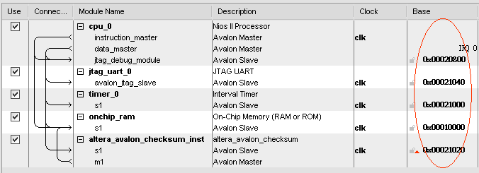
這些都要透過了解Avalon Bus (System interconnect fabric)來解決,以下是整個硬體電路的架構圖:
整個custom component在硬體電路分成兩部分:
1.淺藍色的Task Logic:
Checksum Task Logic:使用Verilog實踐整個checksum演算法,這部分我們已經解決。
2.深藍色的Interface:
Avalon-MM Master Interface:讓FPGA能讀取記憶體內的資料。
Avalon-MM Slave Interface:讓C能將資料傳給Verilog,讓Verilog能將資料傳給C。
我們可以發現,checksum master component因此是個同時有master,也同時有slave interface的component。
Checksum Master component完整架構
一個完整的SOPC component包含三個部分:
1.由Verilog描述如上圖的硬體。
2.由SOPC Builder產生_hw.tcl將Verilog打包成合乎Avalon Bus規格的元件。
3.由C的macro所提供的register map與software API。
整個component的檔案說明如下
| 檔案 | 敘述 | 軟硬 |
| /altera_avalon_checksum | 包含整個component的最上層目錄 | 目錄 |
| /altera_avalon_checksum/altera_avalon_checksum.v | Verilog的top module,負責建立task logic、master、slave | 硬體 |
| /altera_avalon_checksum/checksum_task_logic.v | checksum演算法的硬體電路實現 | 硬體 |
| /altera_avalon_checksum/read_master.v | master interface與讀取master的FSM | 硬體 |
| /altera_avalon_checksum/s1_slave.v | slave interface與讀寫register | 硬體 |
| /altera_avalon_checksum/inc/altera_avalon_checksum_regs.h | register map | 軟體 |
| /altera_avalon_checksum/HAL/inc | software API的header file | 軟體 |
| /altera_avalon_checksum/HAL/src | software API的.c | 軟體 |
| altera_avalon_checksum/checksum_test_software/test_checksum.c | 使用component的範例程式 | 軟體 |
接下來我們就一個一個檔案來深入探討。
altera_avalon_checksum.v / Verilog
2 * *
3 * License Agreement *
4 * *
5 * Copyright (c) 2007 Altera Corporation, San Jose, California, USA. *
6 * All rights reserved. *
7 * *
8 * Permission is hereby granted, free of charge, to any person obtaining a *
9 * copy of this software and associated documentation files (the "Software"), *
10 * to deal in the Software without restriction, including without limitation *
11 * the rights to use, copy, modify, merge, publish, distribute, sublicense, *
12 * and/or sell copies of the Software, and to permit persons to whom the *
13 * Software is furnished to do so, subject to the following conditions: *
14 * *
15 * The above copyright notice and this permission notice shall be included in *
16 * all copies or substantial portions of the Software. *
17 * *
18 * THE SOFTWARE IS PROVIDED "AS IS", WITHOUT WARRANTY OF ANY KIND, EXPRESS OR *
19 * IMPLIED, INCLUDING BUT NOT LIMITED TO THE WARRANTIES OF MERCHANTABILITY, *
20 * FITNESS FOR A PARTICULAR PURPOSE AND NONINFRINGEMENT. IN NO EVENT SHALL THE *
21 * AUTHORS OR COPYRIGHT HOLDERS BE LIABLE FOR ANY CLAIM, DAMAGES OR OTHER *
22 * LIABILITY, WHETHER IN AN ACTION OF CONTRACT, TORT OR OTHERWISE, ARISING *
23 * FROM, OUT OF OR IN CONNECTION WITH THE SOFTWARE OR THE USE OR OTHER *
24 * DEALINGS IN THE SOFTWARE. *
25 * *
26 * This agreement shall be governed in all respects by the laws of the State *
27 * of California and by the laws of the United States of America. *
28 * *
29 ******************************************************************************/
30
31 module altera_avalon_checksum (
32 //Avalon clock interface siganals
33 input csi_clockreset_clk,
34 input csi_clockreset_reset_n,
35 //Signals for Avalon-MM slave port
36 input [2:0] avs_s1_address,
37 input avs_s1_chipselect_n,
38 input avs_s1_read_n,
39 input avs_s1_write_n,
40 input [31:0] avs_s1_writedata,
41 output [31:0] avs_s1_readdata,
42 //Signals for read only Avalon-MM master port
43 output [31:0] avm_m1_address,
44 output [3:0] avm_m1_byteenable,
45 output avm_m1_read_n,
46 input [31:0] avm_m1_readdata,
47 input avm_m1_waitrequest
48 );
49
50 // Signals from s1_slave
51 wire [31:0] addr_reg;
52 wire [15:0] len_reg;
53 wire go;
54
55 // Signals for read_master
56 wire read_busy;
57 wire data_in_ready;
58 wire [31:0] incomming_data;
59 wire [15:0] result;
60
61 s1_slave slave_port (
62 //Avalon clock interface siganals
63 .clk(csi_clockreset_clk),
64 .reset_n(csi_clockreset_reset_n),
65 //Signals for Avalon-MM slave port
66 .avs_s1_address(avs_s1_address),
67 .avs_s1_read_n(avs_s1_read_n),
68 .avs_s1_write_n(avs_s1_write_n),
69 .avs_s1_writedata(avs_s1_writedata),
70 .avs_s1_readdata(avs_s1_readdata),
71 .avs_s1_chipselect_n(avs_s1_chipselect_n),
72 //Signals to Avalon-MM master module
73 .addr_reg(addr_reg),
74 .len_reg(len_reg),
75 .go(go),
76 //stop,
77 .read_busy(read_busy), // busy bit
78 .edge_pulse(), // debug port
79 // result from checksum transform
80 .result(result) // data from transform
81 );
82
83 read_master master_port (
84 //Avalon clock interface siganals
85 .clk(csi_clockreset_clk),
86 .reset_n(csi_clockreset_reset_n),
87 //Signals for Avalon-MM master port
88 .avm_m1_address(avm_m1_address),
89 .avm_m1_byteenable(avm_m1_byteenable), //for byte level control
90 .avm_m1_read_n(avm_m1_read_n),
91 .avm_m1_readdata(avm_m1_readdata),
92 .avm_m1_waitrequest(avm_m1_waitrequest),
93 // Signals from slave registers
94 .addr_reg(addr_reg),
95 .len_reg(len_reg),
96 .go(go),
97 // Signals to slave registers
98 .read_busy(read_busy),
99 // Signals to checksum task logic
100 .data_in_ready(data_in_ready), // debug port
101 .data_to_process(incomming_data) //read master data to transform
102 );
103
104 checksum_task_logic transform (
105 .clk(csi_clockreset_clk),
106 .reset_n(csi_clockreset_reset_n),
107 .go(go),
108 .data_in_ready(data_in_ready),
109 .data_to_process(incomming_data),
110 .result(result)
111 );
112
113 endmodule
altera_avalon_checksum是整個component的top module,目的只在於包含master與slave interface,以及對master、slave與task logic做例化。一個好的top module其實也該如此,目的只是對其他module做例化與連線的動作,而不實作其他的功能,這種風格相當於Design Pattern的Facade Pattern,儘管整個Component內部有很多module,但對於外部來說,只認知top module的interface。若你熟悉上一代的PWM範例,altera_avalon_checksum.v相當於pwm_avalon_interface.v的地位。
altera_avalon_checksum一共包含3個interface:
Avalon-MM Clock Interface
Avalon-MM Master Interface
Avalon-MM Slave Interface
這3個interface皆參考(筆記) Naming Convention for Avalon Signal Type (IC Design) (SOPC Builder),這也是上一代PWM範例所沒有的。這樣的好處是將來SOPC Builder會自動認出interface type、interface name與signal type,不需再SOPC Builder又設一次,且增加程式碼的可讀性。
Avalon-MM Clock Interface
為了將system clock與reset傳進checksum componen供master與slave同步使用,所以包含了Avalon-MM clock interface,在SOPC Builder的Interface tab中,clock interface將連接到master與slave interface。
| Signal Name in HDL | Avalon-MM Signal Type | Width | Dir | Notes |
| csi_clockreset_clk | clk | 1 | in | checksum component所用到的同步clock |
| csi_clockreset_reset_n | reset_n | 1 | in | checksum component所用到的非同步reset |
Avalon-MM Master Interface
為了讓checksum component從記憶體中讀取資料,所以包含了Avalon-MM master interface,它有幾個特色:
1.與clock interface同步。
2.對system interconnect fabric發起master transfer,這也是選擇使用master interface最重要的原因。
| Signal Name in HDL | Avalon-MM Signal Type | Width | Dir | Notes |
| avm_m1_address | address | 32 | out | |
| avm_m1_byteenable | byteenable | 4 | out | |
| avm_m1_read_n | read_n | 1 | out | read request信號 |
| avm_m1_readdata | readdata | 32 | in | 從記憶體讀進的資料 |
| avm_m1_waitrequest | waitrequest | 1 | in | 強迫master port做等待,直到system interconnect fabric準備開始傳輸資料。 |
Avalon-MM Slave Interface
為了讓軟硬體能透過Avalon bus讀寫register,所以包含了Avalon-MM slave interface,它有幾個特色:
1.與clock interface同步。
2.可從slave port讀出資料,也可將資料寫進slave port。
3.使用Native address alignment,因為slave port是直接連到register而非記憶體裝置。
| Signal Name in HDL | Avalon-MM Signal Type | Width | Dir | Notes |
| avs_s1_address | address | 3 | in | readdata與writedata資料的offset |
| avs_s1_read_n | read_n | 1 | in | read request信號 |
| avs_s1_write_n | write_n | 1 | in | write request信號 |
| avs_s1_chipselect | chipselect_n | 1 | in | slave port的chip select信號。除非chip_select_n enable,否則將忽略所有信號 |
| avs_s1_readdata | readdata | 32 | out | 從slave讀出資料 |
| avs_s1_writedata | writedata | 32 | in | 將資料寫進slave |
Avalon-MM Slave Interface的實現
altera_avalon_checksum.v包含了Avalon-MM Slave Interface,但並沒有包含其實現(implementation),其實現要靠s1_slave.v來完成, 它相當於前一代PWM範例的pwm_register_file.v的地位,所以你也可以將s1_slave.v當成register file來理解。
實現slave interface可以解決以下問題:
1..如何由C告訴FPGA記憶體位址,0xf0個數?
2.FPGA計算完checksum後,該如何將計算結果的0x5a5a傳給C?
s1_slave.v / Verilog
2 * *
3 * License Agreement *
4 * *
5 * Copyright (c) 2007 Altera Corporation, San Jose, California, USA. *
6 * All rights reserved. *
7 * *
8 * Permission is hereby granted, free of charge, to any person obtaining a *
9 * copy of this software and associated documentation files (the "Software"), *
10 * to deal in the Software without restriction, including without limitation *
11 * the rights to use, copy, modify, merge, publish, distribute, sublicense, *
12 * and/or sell copies of the Software, and to permit persons to whom the *
13 * Software is furnished to do so, subject to the following conditions: *
14 * *
15 * The above copyright notice and this permission notice shall be included in *
16 * all copies or substantial portions of the Software. *
17 * *
18 * THE SOFTWARE IS PROVIDED "AS IS", WITHOUT WARRANTY OF ANY KIND, EXPRESS OR *
19 * IMPLIED, INCLUDING BUT NOT LIMITED TO THE WARRANTIES OF MERCHANTABILITY, *
20 * FITNESS FOR A PARTICULAR PURPOSE AND NONINFRINGEMENT. IN NO EVENT SHALL THE *
21 * AUTHORS OR COPYRIGHT HOLDERS BE LIABLE FOR ANY CLAIM, DAMAGES OR OTHER *
22 * LIABILITY, WHETHER IN AN ACTION OF CONTRACT, TORT OR OTHERWISE, ARISING *
23 * FROM, OUT OF OR IN CONNECTION WITH THE SOFTWARE OR THE USE OR OTHER *
24 * DEALINGS IN THE SOFTWARE. *
25 * *
26 * This agreement shall be governed in all respects by the laws of the State *
27 * of California and by the laws of the United States of America. *
28 * *
29 ******************************************************************************/
30
31 module s1_slave (
32 // Global Avalon interface siganals
33 input clk,
34 input reset_n,
35 // Signals for Avalon-MM slave port
36 input [2:0] avs_s1_address,
37 input avs_s1_read_n,
38 input avs_s1_write_n,
39 input [31:0] avs_s1_writedata,
40 output [31:0] avs_s1_readdata,
41 input avs_s1_chipselect_n,
42 // Signals Avalon-MM master module
43 // to master
44 output reg [31:0] addr_reg,
45 output reg [15:0] len_reg,
46 output go,
47 // from master
48 input read_busy, // busy bit
49 // to task logic
50 input [15:0] result, // Signals transform
51 output edge_pulse // debug -- look for busy bit transition
52 );
53
54 // define the write register offsets
55 parameter ADDR = 3'b000,
56 LEN = 3'b001,
57 CNTL = 3'b010,
58 RESERVED1 = 3'b011;
59
60 // Define the read register offsets
61 parameter RESULT = 3'b100,
62 STATUS = 3'b101,
63 RESERVED2 = 3'b110,
64 RESERVED3 = 3'b111;
65
66 // Module contents
67 wire [31:0] result_32;
68 wire [31:0] status_32;
69
70 reg [2:0] cntl_reg;
71 reg read_done;
72 reg edge_detect_reg;
73 reg [31:0] read_data_reg;
74
75 // drive GO bit from control register
76 assign go = cntl_reg[0];
77
78 // Assigns read_data_reg to the slave readdata port
79 assign avs_s1_readdata = read_data_reg;
80
81 // Looks for negitive edge transition of busy bit compared to previous clock value
82 assign edge_pulse = !(read_busy | !edge_detect_reg);
83
84 // create write register block
85 always @ (posedge clk or negedge reset_n) begin
86 if (reset_n == 1'b0) begin
87 addr_reg <= 32'h00000000;
88 len_reg <= 16'h0000;
89 cntl_reg <= 3'b000;
90 //read_done <= 1'b1;
91 end
92 else begin
93 if (avs_s1_chipselect_n == 1'b0 & avs_s1_write_n == 1'b0) begin // write cycle to slave registers
94 case (avs_s1_address[2:0])
95 ADDR:
96 if (!read_busy)
97 addr_reg <= avs_s1_writedata[31:0];
98 else
99 addr_reg <= addr_reg;
100
101 LEN:
102 if (!read_busy)
103 len_reg <= avs_s1_writedata[15:0];
104 else
105 len_reg <= len_reg;
106
107 CNTL:
108 if (!read_busy)
109 cntl_reg <= avs_s1_writedata[2:0];
110 else
111 cntl_reg <= cntl_reg;
112
113 default: begin
114 addr_reg <= addr_reg;
115 len_reg <= len_reg;
116 cntl_reg <= cntl_reg;
117 end
118 endcase
119 end
120
121 if (go) // clear go bit after asserted one clock cycle
122 cntl_reg[0] <= 1'b0;
123
124 end
125 end
126
127 // Create read register block
128 always @ (posedge clk or negedge reset_n) begin
129 if (reset_n == 1'b0)
130 read_data_reg <= 32'b0;
131 else
132 read_data_reg <= (avs_s1_address == LEN) ? { 16'h0000, len_reg[15:0] } :
133 (avs_s1_address == CNTL) ? { 28'h00000000, cntl_reg[2:0] } :
134 (avs_s1_address == RESULT) ? { 16'h000, result[15:0]} :
135 (avs_s1_address == STATUS) ? { 30'h00000000, read_done, read_busy } :
136 addr_reg;
137 end
138
139
140 // negitive edge detect circuit to generate read_done bit from busy bit
141 always @ (posedge clk or negedge reset_n) begin
142 if (reset_n == 1'b0)
143 edge_detect_reg <= 1'b0;
144 else if (clk == 1'b1)
145 edge_detect_reg <= read_busy;
146 end
147
148 always@(posedge clk or negedge reset_n) begin
149 if (reset_n == 1'b0)
150 read_done <= 1'b0;
151 else if (edge_pulse) // asserts DONE bit when edge detected
152 read_done <= 1'b1;
153 else if (go) // clear done bit when GO bit asserted
154 read_done <= 1'b0;
155 else
156 read_done <= read_done;
157 end
158
159 endmodule
32行
input clk,
input reset_n,
實現clock interface
35行
input [2:0] avs_s1_address,
input avs_s1_read_n,
input avs_s1_write_n,
input [31:0] avs_s1_writedata,
output [31:0] avs_s1_readdata,
input avs_s1_chipselect_n,
實現slave interface
43行
// to master
output reg [31:0] addr_reg,
output reg [15:0] len_reg,
output go,
由整個checksum master component的硬體架構圖可得知,slave的功能除了當Nios II軟體與FPGA硬體的溝通媒介外,它與master與task logic之間仍有信號傳遞,addr_reg、len_reg、go三個port就是將信號送至master。
47行
input read_busy, // busy bit
read_busy是從master讀進信號,表示master正在從記憶體讀取資料。
49行
input [15:0] result, // Signals transform
result是從checksum_task_logic傳進0x5a5a的結果,以便最後再送回Nios II的C。
前面提到s1_slave.v也可視為register file,因為主要就是要處理這些register,先討論write register,也就是當資料寫進slave後,將資料存在register內。這裡有addr_reg、len_reg、cntl_reg 3個write register,最後會將這3個值傳給master。
84行
always @ (posedge clk or negedge reset_n) begin
if (reset_n == 1'b0) begin
addr_reg <= 32'h00000000;
len_reg <= 16'h0000;
cntl_reg <= 3'b000;
//read_done <= 1'b1;
end
else begin
if (avs_s1_chipselect_n == 1'b0 & avs_s1_write_n == 1'b0) begin // write cycle to slave registers
case (avs_s1_address[2:0])
ADDR:
if (!read_busy)
addr_reg <= avs_s1_writedata[31:0];
else
addr_reg <= addr_reg;
LEN:
if (!read_busy)
len_reg <= avs_s1_writedata[15:0];
else
len_reg <= len_reg;
CNTL:
if (!read_busy)
cntl_reg <= avs_s1_writedata[2:0];
else
cntl_reg <= cntl_reg;
default: begin
addr_reg <= addr_reg;
len_reg <= len_reg;
cntl_reg <= cntl_reg;
end
endcase
end
if (go) // clear go bit after asserted one clock cycle
cntl_reg[0] <= 1'b0;
end
end
整段在處理write register,我們細部的來研究其過程。
93行
根據Avalon的規定,一定要chipselect_n為0且write_n為0時,此時writedata上的資料才是合法的。
96行
addr_reg <= avs_s1_writedata[31:0];
else
addr_reg <= addr_reg;
read_busy是由master傳給slave,表示master正在從記憶體讀取資料,這時slave就先等master,一直到master讀取完畢,再從writedata寫入write register。
既然寫入slave的資料都在writedata上,slave要怎麼判斷是addr_reg、len_reg、cntl_reg呢?我們知道每個SOPC Component最後都會由SOPC Builder分配一個base address,透過不同的offset,我們可以從Nios II用C語言傳資料進slave,而這個offset,就是傳進slave的address input port。
54行
parameter ADDR = 3'b000,
LEN = 3'b001,
CNTL = 3'b010,
RESERVED1 = 3'b011;
定義出各write register的offset,這些定義,在altera_avalon_checksum_regs.h也完全一樣。
#define IOWR_ALTERA_AVALON_CHECKSUM_LENGTH(base, data) IOWR(base, 1, data)
#define IOWR_ALTERA_AVALON_CHECKSUM_CTRL(base, data) IOWR(base, 2, data)
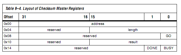
在這順便澄清一個觀念,這裡的3'b000、3'b001....,不是bit也不是byte,也不代表實際register的offset,而是代表n個32 bit,請看下圖。
上表的offset,才是真的以byte為單位的offset,因為都是以32 bit定址,所以每個register皆間距4 byte,也就是32 bit,所以才說3'b000、3'b001代表的是n個32 bit。或許你會問,length與result才16 bit而已,怎麼存在32 bit的空間呢?請看下圖。
只有address因為32 bit,所以用滿了,length與result都因為只有16 bit,所以剩下的16 bit沒用到而是reserved,至於GO、DONE、BUSY更慘,只用到1到2 bit,這個問題最後會在register map,也就是altera_avalon_checksum_regs.h討論。
看完write register,接著來看read register,這是一個反過來的思維,是將資料準備好後,讓其他component從slave讀出資料,在這裡就是Nios II的C語言從slave讀回資料。 同樣的需判斷address的offset,決定要送出什麼資料出去。
127行
always @ (posedge clk or negedge reset_n) begin
if (reset_n == 1'b0)
read_data_reg <= 32'b0;
else
read_data_reg <= (avs_s1_address == LEN) ? { 16'h0000, len_reg[15:0] } :
(avs_s1_address == CNTL) ? { 28'h00000000, cntl_reg[2:0] } :
(avs_s1_address == RESULT) ? { 16'h000, result[15:0]} :
(avs_s1_address == STATUS) ? { 30'h00000000, read_done, read_busy } :
addr_reg;
end
整段在處理read register,我們細部的來研究其過程。
60行
#define IORD_ALTERA_AVALON_CHECKSUM_LENGTH(base) IORD(base, 1)
#define IORD_ALTERA_AVALON_CHECKSUM_CTRL(base) IORD(base, 2)
#define IORD_ALTERA_AVALON_CHECKSUM_RESULT(base) IORD(base, 4)
#define IORD_ALTERA_AVALON_CHECKSUM_STATUS(base) IORD(base, 5)
定義出各read register的offset,已經定義過的offset就不重複定義了,這些定義,在altera_avalon_checksum_regs.h也完全一樣。
parameter RESULT = 3'b100,
STATUS = 3'b101,
RESERVED2 = 3'b110,
RESERVED3 = 3'b111;
slave最後一個任務,就是告訴Nios II的C語言,到底硬體電路算好checksum了沒?C會不斷的polling slave詢問目前的status,到底是busy還是已經已經讀完為done。busy很簡單,只要從master傳來的read_busy是1就是busy,當read_busy一從1變0時,就表示已經done了。之前模擬的波形圖發現,3個clock花在讀取記憶體,第一個clock因為要設定sum_reg的初始值,在第4個clock就可以看到結果,也就是說,其實真的計算並沒有花到clock,只要從記憶體讀取完畢,也代表checksum已經求出來了。所以我們需要一個下緣微分電路(negtive edge detection circuit)判斷是否已經從記體體讀取完畢,以此告訴Nios II的C已經求出checksum了。
140行
always @ (posedge clk or negedge reset_n) begin
if (reset_n == 1'b0)
edge_detect_reg <= 1'b0;
else if (clk == 1'b1)
edge_detect_reg <= read_busy;
end
81行
assign edge_pulse = !(read_busy | !edge_detect_reg);
這是一個基本的電路,我就不再多說,請參閱(筆記) 如何設計邊緣檢測電路? (SOC) (Verilog) 。
148行
if (reset_n == 1'b0)
read_done <= 1'b0;
else if (edge_pulse) // asserts DONE bit when edge detected
read_done <= 1'b1;
else if (go) // clear done bit when GO bit asserted
read_done <= 1'b0;
else
read_done <= read_done;
end
當edge_pulse為1,表示測到read_busy由1變0,表示已經讀完,所以read_done為1,當go信號為1時,表示正要開始計算,所以read_done為0。
132行
(avs_s1_address == CNTL) ? { 28'h00000000, cntl_reg[2:0] } :
(avs_s1_address == RESULT) ? { 16'h000, result[15:0]} :
(avs_s1_address == STATUS) ? { 30'h00000000, read_done, read_busy } :
addr_reg;
最後read_busy與read_done合併,送出目前的status,這樣Nios II的C就能去polling目前的status,判斷是否計算完畢。
在test_checksum.c的50行
while (!(status & ALTERA_AVALON_CHECKSUM_STATUS_DONE_MSK))
status = IORD_ALTERA_AVALON_CHECKSUM_STATUS(ALTERA_AVALON_CHECKSUM_INST_BASE);
可以看到C不斷的去polling status是否為read_done,判斷FPGA是否已經計算完畢了。
Avalon-MM Master Interface的實現
altera_avalon_checksum.v包含了Avalon-MM Master Interface,但並沒有包含其實現(implementation),其實現要靠read_master.v來完成, 在前一代PWM範例並沒有示範master寫法,示範master interface也是checksum master範例的一大特色。
實現master interface可以解決以下問題:
1.FPGA該如何讀取記憶體的12個0xf0?無論你是放在on-chip memory、SRAM或者SDRAM。
read_master.v / Verilog
2 * *
3 * License Agreement *
4 * *
5 * Copyright (c) 2007 Altera Corporation, San Jose, California, USA. *
6 * All rights reserved. *
7 * *
8 * Permission is hereby granted, free of charge, to any person obtaining a *
9 * copy of this software and associated documentation files (the "Software"), *
10 * to deal in the Software without restriction, including without limitation *
11 * the rights to use, copy, modify, merge, publish, distribute, sublicense, *
12 * and/or sell copies of the Software, and to permit persons to whom the *
13 * Software is furnished to do so, subject to the following conditions: *
14 * *
15 * The above copyright notice and this permission notice shall be included in *
16 * all copies or substantial portions of the Software. *
17 * *
18 * THE SOFTWARE IS PROVIDED "AS IS", WITHOUT WARRANTY OF ANY KIND, EXPRESS OR *
19 * IMPLIED, INCLUDING BUT NOT LIMITED TO THE WARRANTIES OF MERCHANTABILITY, *
20 * FITNESS FOR A PARTICULAR PURPOSE AND NONINFRINGEMENT. IN NO EVENT SHALL THE *
21 * AUTHORS OR COPYRIGHT HOLDERS BE LIABLE FOR ANY CLAIM, DAMAGES OR OTHER *
22 * LIABILITY, WHETHER IN AN ACTION OF CONTRACT, TORT OR OTHERWISE, ARISING *
23 * FROM, OUT OF OR IN CONNECTION WITH THE SOFTWARE OR THE USE OR OTHER *
24 * DEALINGS IN THE SOFTWARE. *
25 * *
26 * This agreement shall be governed in all respects by the laws of the State *
27 * of California and by the laws of the United States of America. *
28 * *
29 ******************************************************************************/
30
31 module read_master (
32 // Global Avalon interface siganals
33 input clk,
34 input reset_n,
35 // Signals for Avalon-MM master port
36 output [31:0] avm_m1_address,
37 output [3:0] avm_m1_byteenable, // for future byte lane control
38 output reg avm_m1_read_n,
39 input [31:0] avm_m1_readdata,
40 input avm_m1_waitrequest,
41 output reg [3:0] avm_m1_byteenable_mask, // debug - for byteenable mask values
42 // Signals from slave registers
43 input [31:0] addr_reg,
44 input [15:0] len_reg,
45 input go,
46 // Signals to slave registers
47 output reg read_busy,
48 // Signals to checksum task logic
49 output data_in_ready,
50 output [15:0] count, // debug - check count value and for future enhancement
51 output [31:0] data_to_process
52 );
53
54 assign avm_m1_address = { addr[31:2], 2'b0 }; // Lower address bits are not used assume world aligned addresses
55 // Check for valid read data on the master port by looking for waitrequest with each read
56 assign data_in_ready = ( (avm_m1_read_n == 1'b0) && !avm_m1_waitrequest) ? 1'b1 : 1'b0;
57 assign avm_m1_byteenable = 4'b1111; // drive byteenables high
58
59 reg [31:0] addr;
60 reg [15:0] count_tmp;
61
62 assign count = count_tmp;
63 // passing readdata to task logic
64 // mask data to process based on byteenable mask
65 assign data_to_process[31:0] = (avm_m1_byteenable_mask == 4'b0001) ? ( 32'h000000FF & avm_m1_readdata[31:0]) :
66 (avm_m1_byteenable_mask == 4'b0011) ? ( 32'h0000FFFF & avm_m1_readdata[31:0]) :
67 (avm_m1_byteenable_mask == 4'b0111) ? ( 32'h00FFFFFF & avm_m1_readdata[31:0]) :
68 avm_m1_readdata[31:0];
69
70 //Statemachine block for controlling read master signals
71 always@(posedge clk or negedge reset_n) begin
72 if (reset_n == 1'b0) begin
73 count_tmp <= 'b0;
74 read_busy <= 1'b0;
75 addr <= 'b0;
76 avm_m1_byteenable_mask <= 4'b0000;
77 avm_m1_read_n <= 1'b1;
78 read_busy <= 1'b0;
79 end
80 else if (go) begin // loads count and start read master statemachine
81 count_tmp <= len_reg - 3'h4; // decrement count for this initial load/read state
82 addr <= addr_reg ; // loads address - must be 32-bit word aligned addess
83 avm_m1_byteenable_mask <= 4'b1111;
84 avm_m1_read_n <= 1'b1;
85 read_busy <= 1'b1;
86 end
87 else if (count > 3 && data_in_ready) begin // Main loop for read master statemachine
88 count_tmp <= count_tmp - 3'h4;
89 addr <= addr + 3'h4;
90 avm_m1_byteenable_mask <= 4'b1111; // assert byteenable mask byte lane(s) 3,2,1,0
91 avm_m1_read_n <= 1'b0;
92 read_busy <= 1'b1;
93 end
94 else if (count == 3 && data_in_ready) begin// Last read for un-aligned word lengths - 3 bytes
95 count_tmp <= count_tmp - 3'h3;
96 addr <= addr + 3'h4;
97 avm_m1_byteenable_mask <= 4'b0111; // assert byteenable mask byte lane(s) 2,1,0
98 avm_m1_read_n <= 1'b0;
99 read_busy <= 1'b1;
100 end
101 else if (count == 2 && data_in_ready) begin// Last read for un-aligned word lengths - 2 bytes
102 count_tmp <= count_tmp - 3'h2;
103 addr <= addr + 3'h4;
104 avm_m1_byteenable_mask <= 4'b0011; // assert byteenable mask byte lane(s) 1,0
105 avm_m1_read_n <= 1'b0;
106 read_busy <= 1'b1;
107 end
108 else if (count == 1 && data_in_ready) begin// Last read for un-aligned word lengths - 1 bytes
109 count_tmp <= count_tmp - 3'h1;
110 addr <= addr + 3'h4;
111 avm_m1_byteenable_mask <= 4'b0001; // assert byteenable mask byte lane(s) 0
112 avm_m1_read_n <= 1'b0;
113 read_busy <= 1'b1;
114 end
115 else if (count ==0 && !data_in_ready) begin // Hold outputs if waitrequest asserted during last read cycle
116 count_tmp <= count_tmp;
117 addr <= addr ;
118 avm_m1_byteenable_mask <= avm_m1_byteenable_mask;
119 avm_m1_read_n <= avm_m1_read_n;
120 read_busy <= read_busy;
121 end
122 else if (count ==0) begin // byte count is zero and the exit condition for read master statemachine
123 addr <= 'b0; // clear address
124 avm_m1_byteenable_mask <= 4'b0000;// clear byteenables
125 avm_m1_read_n <= 1'b1; // stop reading
126 read_busy <= 1'b0; // deassert busy bit
127 end
128 else begin // Starts the read cycle after a load or holds master outputs static when waitrequest asserted
129 count_tmp <= count_tmp;
130 addr <= addr ;
131 avm_m1_byteenable_mask <= avm_m1_byteenable_mask;
132 avm_m1_read_n <= 1'b0; // starts the read cycle
133 read_busy <= 1'b1;
134 end
135 end
136
137 endmodule
32行
input clk,
input reset_n,
實現clock interface
35行
output [31:0] avm_m1_address,
output [3:0] avm_m1_byteenable, // for future byte lane control
output reg avm_m1_read_n,
input [31:0] avm_m1_readdata,
input avm_m1_waitrequest,
output reg [3:0] avm_m1_byteenable_mask, // debug - for byteenable mask values
實現master interface
42行
input [31:0] addr_reg,
input [15:0] len_reg,
input go,
由整的checksum master component的硬體架構圖可得知,master的功能除了對記憶體讀取資料外,它與slave與task logic之間仍有信號傳遞,addr_reg、len_reg、go三個port就是將信號送slave傳進來的。
46行
output reg read_busy,
read_busy是將信號傳給slave,表示正在從記憶體讀取資料。
48行
output data_in_ready,
output [15:0] count, // debug - check count value and for future enhancement
output [31:0] data_to_process
當master從記憶體抓到資料後,最重要的就是將資料傳給task logic做運算,data_in_ready表示資料是否合法,data_to_process則是32 bit的資料。
現在我們就來看看data_in_ready與data_to_process是如何產生的。
54行
assign data_in_ready = ( (avm_m1_read_n == 1'b0) && !avm_m1_waitrequest) ? 1'b1 : 1'b0;
data_in_ready是由avm_m1_read_n與avm_m1_waitrequest共同決定。當avm_m1_read_n為0表示master對avalon bus送出要求讀取資料信號,avm_m1_request則是avalon bus arbiter傳給master的信號,若有多個master同時求讀取記憶體,avalon bus arbiter會做出仲裁,決定讓哪一個master讀取,哪一個master等待,當收到avm_m1_waitrequest為1時,master必須等待,當收到avm_m1_waitrequest為0時,表示可以讀取記憶體,所以必須同時avm_m1_read_n為0且avm_m1_request為0時,data_in_ready才能為1。
之前討論slave時,slave是靠avs_s1_address(也就是offset)來從avs_s1_writedata分析出寫入slave的資料,雖然master也有avm_m1_address,不過avm_m1_address卻是個output,是要傳給avalon bus,而不是自己要用的,那master要如何從avm_m1_readdata分析出資料給data_to_process呢?
還記得在test_checksum.c的45行,我們曾經在C語言傳記憶體位址address、資料長度length與開始計算go給slave
test_checksum.c 45行
printf("Writing to address register. \n");
IOWR_ALTERA_AVALON_CHECKSUM_ADDR(ALTERA_AVALON_CHECKSUM_INST_BASE, ONCHIP_RAM_BASE);
/* Store the length in bytes (up to a 16-bit value). */
printf("Writing to length register. \n");
IOWR_ALTERA_AVALON_CHECKSUM_LENGTH(ALTERA_AVALON_CHECKSUM_INST_BASE, len);
/* Tell it to "go". */
printf("Writing to go bit in control register. \n");
IOWR_ALTERA_AVALON_CHECKSUM_CTRL(ALTERA_AVALON_CHECKSUM_INST_BASE+ALTERA_AVALON_CHECKSUM_CTRL_GO_OFST, ALTERA_AVALON_CHECKSUM_CTRL_GO_MSK);
這3個信號,其實在slave中都還沒開始用,slave只是乖乖的放進write register,然後傳給master。其中的addr在read_master.v的54行
透過avm_m1_address傳給avalon bus。而length與go,就是要用來從avm_m1_readdata中,分析資料給data_to_process。
70行
always@(posedge clk or negedge reset_n) begin
if (reset_n == 1'b0) begin
count_tmp <= 'b0;
read_busy <= 1'b0;
addr <= 'b0;
avm_m1_byteenable_mask <= 4'b0000;
avm_m1_read_n <= 1'b1;
read_busy <= 1'b0;
end
else if (go) begin // loads count and start read master statemachine
count_tmp <= len_reg - 3'h4; // decrement count for this initial load/read state
addr <= addr_reg ; // loads address - must be 32-bit word aligned addess
avm_m1_byteenable_mask <= 4'b1111;
avm_m1_read_n <= 1'b1;
read_busy <= 1'b1;
end
else if (count > 3 && data_in_ready) begin // Main loop for read master statemachine
count_tmp <= count_tmp - 3'h4;
addr <= addr + 3'h4;
avm_m1_byteenable_mask <= 4'b1111; // assert byteenable mask byte lane(s) 3,2,1,0
avm_m1_read_n <= 1'b0;
read_busy <= 1'b1;
end
else if (count == 3 && data_in_ready) begin// Last read for un-aligned word lengths - 3 bytes
count_tmp <= count_tmp - 3'h3;
addr <= addr + 3'h4;
avm_m1_byteenable_mask <= 4'b0111; // assert byteenable mask byte lane(s) 2,1,0
avm_m1_read_n <= 1'b0;
read_busy <= 1'b1;
end
else if (count == 2 && data_in_ready) begin// Last read for un-aligned word lengths - 2 bytes
count_tmp <= count_tmp - 3'h2;
addr <= addr + 3'h4;
avm_m1_byteenable_mask <= 4'b0011; // assert byteenable mask byte lane(s) 1,0
avm_m1_read_n <= 1'b0;
read_busy <= 1'b1;
end
else if (count == 1 && data_in_ready) begin// Last read for un-aligned word lengths - 1 bytes
count_tmp <= count_tmp - 3'h1;
addr <= addr + 3'h4;
avm_m1_byteenable_mask <= 4'b0001; // assert byteenable mask byte lane(s) 0
avm_m1_read_n <= 1'b0;
read_busy <= 1'b1;
end
else if (count ==0 && !data_in_ready) begin // Hold outputs if waitrequest asserted during last read cycle
count_tmp <= count_tmp;
addr <= addr ;
avm_m1_byteenable_mask <= avm_m1_byteenable_mask;
avm_m1_read_n <= avm_m1_read_n;
read_busy <= read_busy;
end
else if (count ==0) begin // byte count is zero and the exit condition for read master statemachine
addr <= 'b0; // clear address
avm_m1_byteenable_mask <= 4'b0000;// clear byteenables
avm_m1_read_n <= 1'b1; // stop reading
read_busy <= 1'b0; // deassert busy bit
end
else begin // Starts the read cycle after a load or holds master outputs static when waitrequest asserted
count_tmp <= count_tmp;
addr <= addr ;
avm_m1_byteenable_mask <= avm_m1_byteenable_mask;
avm_m1_read_n <= 1'b0; // starts the read cycle
read_busy <= 1'b1;
end
end
master讀取avm_m1_readdata的方式是靠SM(state machine)的方式產生avm_m1_byteenable_mask,藉由不同的mask分析出不同的資料,這與slave靠offset的方式有很大的差異,由於avm_m1_readdata的長度為32 bit,也就是4 byte,所以一次可以讀取4個0xf0,在本範例由於12是4的倍數,所以3個clock可讀完,若不是4的倍數,如15,15 % 4 = 3,最後1個clock就可能出現需要從4 byte的avm_m1_readdata中讀取3 byte的資料的情況,所以全部的SM分為以下幾種:(count表示還有幾byte未讀)
| count | 讀取byte |
| > 3 | 一次讀取4 byte |
| == 3 | 一次讀取3 byte |
| == 2 | 一次讀取2 byte |
| == 1 | 一次讀取1 byte |
| == 0 | 讀取完畢,打完收功 |
80行
count_tmp <= len_reg - 3'h4; // decrement count for this initial load/read state
addr <= addr_reg ; // loads address - must be 32-bit word aligned addess
avm_m1_byteenable_mask <= 4'b1111;
avm_m1_read_n <= 1'b1;
read_busy <= 1'b1;
end
go表示開始整個SM,因為一次讀取4 byte,所以count_tmp一次減了3'h4,而avm_m1_byteenable_mask也是4'b1111,表示一次讀取32 bit。 不過由於這個clock只是在設定初始值,還沒有真正的要讀取記憶體,真正的讀取是在下一個clock的SM,所以avm_m1_read_n為1。
87行
count_tmp <= count_tmp - 3'h4;
addr <= addr + 3'h4;
avm_m1_byteenable_mask <= 4'b1111; // assert byteenable mask byte lane(s) 3,2,1,0
avm_m1_read_n <= 1'b0;
read_busy <= 1'b1;
end
整個master最重要的部分在此,當count > 3時,一次讀取4 byte,所以count_tmp減3'h4,但addr卻要加3'h4,為下一個記憶體位址做準備,此時avm_m1_byteenable_mask還是4'b1111,表示一次讀取4 byte。由於真的要開始讀取記憶體了,所以avm_m1_read_n為0。
94行
count_tmp <= count_tmp - 3'h3;
addr <= addr + 3'h4;
avm_m1_byteenable_mask <= 4'b0111; // assert byteenable mask byte lane(s) 2,1,0
avm_m1_read_n <= 1'b0;
read_busy <= 1'b1;
end
若len不是4的倍數,就可能出現最後一次的avm_m1_readdata不能完全讀取,而只能讀部分的問題,count==3表示最後還有3 byte要讀,所以count_tmp減3,但addr還是要加4,畢竟avm_m1_readdata還是一次讀取4 byte了,最重要的是avm_m1_byteenable_mask, 不再是4'b1111,而是4'b0111,表示只讀取3 byte而已。
其餘的count == 2與count == 1同理,我就不再多加解釋。
122行
addr <= 'b0; // clear address
avm_m1_byteenable_mask <= 4'b0000;// clear byteenables
avm_m1_read_n <= 1'b1; // stop reading
read_busy <= 1'b0; // deassert busy bit
end
無論len為何,最後一定會讀完,所以count最終一定等於0,此時要做收尾的動作,addr歸0,mask歸0,avm_m1_read_n為1停止記憶體讀取動作,read_busy歸0。
115行
 else if (count ==0 && !data_in_ready) begin // Hold outputs if waitrequest asserted during last read cycle count_tmp <= count_tmp; addr <= addr ; avm_m1_byteenable_mask <= avm_m1_byteenable_mask; avm_m1_read_n <= avm_m1_read_n; read_busy <= read_busy;end
之前都在討論data_in_ready的狀況,但別忘了master還有個avm_m1_waitrequest的狀況,也就是說,avalon bus發出avm_m1_waitrequest=1要master稍作等待,因為此時記憶體或其他slave有人在讀取,若此時count == 0已經讀完所有資料,只要將目前reg的值繼續傳下去即可,這問題不大,若count != 0,也就是我仍在讀取記憶體過程中,收到avm_m1_waitrequest怎麼辦呢?
128行
count_tmp <= count_tmp;
addr <= addr ;
avm_m1_byteenable_mask <= avm_m1_byteenable_mask;
avm_m1_read_n <= 1'b0; // starts the read cycle
read_busy <= 1'b1;
end
此時當然count_tmp、addr、avm_m1_byteenable_mask要繼續維持到下一個clock,且繼續對avalon bus提出avm_m1_read_n = 0的讀取記憶體要求,看看有沒有機會再下一個clock讀取記憶體。
65行
// mask data to process based on byteenable mask
assign data_to_process[31:0] = (avm_m1_byteenable_mask == 4'b0001) ? ( 32'h000000FF & avm_m1_readdata[31:0]) :
(avm_m1_byteenable_mask == 4'b0011) ? ( 32'h0000FFFF & avm_m1_readdata[31:0]) :
(avm_m1_byteenable_mask == 4'b0111) ? ( 32'h00FFFFFF & avm_m1_readdata[31:0]) :
avm_m1_readdata[31:0];
之前對count的SM對avm_m1_byteenable_mask所佈的局,在此開花結果,依照不同的avm_m1_byteenable_mask值,分別對avm_m1_readdata做mask,讀取相對應的byte給data_to_process,然後再傳給task logic。
master與slave讀取資料方式比較
| slave | master | |
| 判斷資料是否合法 | avs_s1_chipselect_n == 1'b0 & avs_s1_write_n == 1'b0 | avm_m1_read_n == 1'b0 && !avm_m1_waitrequest |
| 擷取資料方式 | 依照avs_s1_address分辨 | 自行設計SM計算avm_m1_byteenable_mask |
撰寫Register Map
以上總算將checksum master的硬體部分完成,但我們還有最後一個問題要解決:
1.C該如何使用這個component?
使用SOPC Builder時,它已經將每個IP的base address分配好,並存在system_0.ptf中,將來Nios II EDS會根據system_0.ptf中的內容,將base address的資訊寫在\checksum_master_onchip\software\blank_project_0_syslib\Debug\system_description\system.h中。
System.h / C
* altera_avalon_checksum_inst configuration
*
*/
#define ALTERA_AVALON_CHECKSUM_INST_NAME "/dev/altera_avalon_checksum_inst"
#define ALTERA_AVALON_CHECKSUM_INST_TYPE "altera_avalon_checksum"
#define ALTERA_AVALON_CHECKSUM_INST_BASE 0x00021020
#define ALTERA_AVALON_CHECKSUM_INST_SPAN 32
#define ALT_MODULE_CLASS_altera_avalon_checksum_inst altera_avalon_checksum
理論上,有了這些macro,就可以用C來存取checksum master了,不過slave的offset部分,軟體開發人員並不清楚,所以我們會再撰寫一個register map:altera_avalon_checksum_regs.h,這在前一代PWM範例相當於altera_avalon_pwm_regs.h。
altera_avalon_checksum_regs.h / C
2 * *
3 * License Agreement *
4 * *
5 * Copyright (c) 2007 Altera Corporation, San Jose, California, USA. *
6 * All rights reserved. *
7 * *
8 * Permission is hereby granted, free of charge, to any person obtaining a *
9 * copy of this software and associated documentation files (the "Software"), *
10 * to deal in the Software without restriction, including without limitation *
11 * the rights to use, copy, modify, merge, publish, distribute, sublicense, *
12 * and/or sell copies of the Software, and to permit persons to whom the *
13 * Software is furnished to do so, subject to the following conditions: *
14 * *
15 * The above copyright notice and this permission notice shall be included in *
16 * all copies or substantial portions of the Software. *
17 * *
18 * THE SOFTWARE IS PROVIDED "AS IS", WITHOUT WARRANTY OF ANY KIND, EXPRESS OR *
19 * IMPLIED, INCLUDING BUT NOT LIMITED TO THE WARRANTIES OF MERCHANTABILITY, *
20 * FITNESS FOR A PARTICULAR PURPOSE AND NONINFRINGEMENT. IN NO EVENT SHALL THE *
21 * AUTHORS OR COPYRIGHT HOLDERS BE LIABLE FOR ANY CLAIM, DAMAGES OR OTHER *
22 * LIABILITY, WHETHER IN AN ACTION OF CONTRACT, TORT OR OTHERWISE, ARISING *
23 * FROM, OUT OF OR IN CONNECTION WITH THE SOFTWARE OR THE USE OR OTHER *
24 * DEALINGS IN THE SOFTWARE. *
25 * *
26 * This agreement shall be governed in all respects by the laws of the State *
27 * of California and by the laws of the United States of America. *
28 * *
29 ******************************************************************************/
30
31 #ifndef __ALTERA_AVALON_CHECKSUM_REGS_H__
32 #define __ALTERA_AVALON_CHECKSUM_REGS_H__
33
34 #include <io.h>
35
36 /* Basic address, read and write macros. */
37 #define IOADDR_ALTERA_AVALON_CHECKSUM_ADDR(base) __IO_CALC_ADDRESS_NATIVE(base, 0)
38 #define IORD_ALTERA_AVALON_CHECKSUM_ADDR(base) IORD(base, 0)
39 #define IOWR_ALTERA_AVALON_CHECKSUM_ADDR(base, data) IOWR(base, 0, data)
40
41 #define IOADDR_ALTERA_AVALON_CHECKSUM_LENGTH(base) __IO_CALC_ADDRESS_NATIVE(base, 1)
42 #define IORD_ALTERA_AVALON_CHECKSUM_LENGTH(base) IORD(base, 1)
43 #define IOWR_ALTERA_AVALON_CHECKSUM_LENGTH(base, data) IOWR(base, 1, data)
44
45 #define IOADDR_ALTERA_AVALON_CHECKSUM_CTRL(base) __IO_CALC_ADDRESS_NATIVE(base, 2)
46 #define IORD_ALTERA_AVALON_CHECKSUM_CTRL(base) IORD(base, 2)
47 #define IOWR_ALTERA_AVALON_CHECKSUM_CTRL(base, data) IOWR(base, 2, data)
48
49 #define IOADDR_ALTERA_AVALON_CHECKSUM_RESULT(base) __IO_CALC_ADDRESS_NATIVE(base, 4)
50 #define IORD_ALTERA_AVALON_CHECKSUM_RESULT(base) IORD(base, 4)
51
52 #define IOADDR_ALTERA_AVALON_CHECKSUM_STATUS(base) __IO_CALC_ADDRESS_NATIVE(base, 5)
53 #define IORD_ALTERA_AVALON_CHECKSUM_STATUS(base) IORD(base, 5)
54
55 /* Masks. */
56 #define ALTERA_AVALON_CHECKSUM_CTRL_GO_MSK (0x1)
57 #define ALTERA_AVALON_CHECKSUM_STATUS_DONE_MSK (0x2)
58 #define ALTERA_AVALON_CHECKSUM_LENGTH_MSK (0xFFFF)
59 #define ALTERA_AVALON_CHECKSUM_RESULT_MSK (0xFFFF)
60
61 /* Offsets. */
62 #define ALTERA_AVALON_CHECKSUM_CTRL_GO_OFST (0)
63 #define ALTERA_AVALON_CHECKSUM_STATUS_BSY_OFST (0)
64 #define ALTERA_AVALON_CHECKSUM_STATUS_DONE_OFST (1)
65
66 #endif /* __ALTERA_AVALON_CHECKSUM_REGS_H__ */
67
由於C只能面對slave,我們再將記憶拉回slave interface。
slave分read register與write register,read register就是供別人從slave讀取,write register就是供別人寫入slave,由於slave是靠address (offset)來分辨在readdata與writedata上的資料,但C開發人員不見的清楚offset是多少,所以我們提供了IORD與IOWR兩套macro讓C使用,並將offset包在macro內。
altera_avalon_checksum_regs.h / C
#define IOADDR_ALTERA_AVALON_CHECKSUM_ADDR(base) __IO_CALC_ADDRESS_NATIVE(base, 0)
#define IORD_ALTERA_AVALON_CHECKSUM_ADDR(base) IORD(base, 0)
#define IOWR_ALTERA_AVALON_CHECKSUM_ADDR(base, data) IOWR(base, 0, data)
#define IOADDR_ALTERA_AVALON_CHECKSUM_LENGTH(base) __IO_CALC_ADDRESS_NATIVE(base, 1)
#define IORD_ALTERA_AVALON_CHECKSUM_LENGTH(base) IORD(base, 1)
#define IOWR_ALTERA_AVALON_CHECKSUM_LENGTH(base, data) IOWR(base, 1, data)
#define IOADDR_ALTERA_AVALON_CHECKSUM_CTRL(base) __IO_CALC_ADDRESS_NATIVE(base, 2)
#define IORD_ALTERA_AVALON_CHECKSUM_CTRL(base) IORD(base, 2)
#define IOWR_ALTERA_AVALON_CHECKSUM_CTRL(base, data) IOWR(base, 2, data)
#define IOADDR_ALTERA_AVALON_CHECKSUM_RESULT(base) __IO_CALC_ADDRESS_NATIVE(base, 4)
#define IORD_ALTERA_AVALON_CHECKSUM_RESULT(base) IORD(base, 4)
#define IOADDR_ALTERA_AVALON_CHECKSUM_STATUS(base) __IO_CALC_ADDRESS_NATIVE(base, 5)
#define IORD_ALTERA_AVALON_CHECKSUM_STATUS(base) IORD(base, 5)
容我再囉嗦一次,這些offset在s1_slave.v的54行都看的到相同的定義
parameter ADDR = 3'b000,
LEN = 3'b001,
CNTL = 3'b010,
RESERVED1 = 3'b011;
// Define the read register offsets
parameter RESULT = 3'b100,
STATUS = 3'b101,
RESERVED2 = 3'b110,
RESERVED3 = 3'b111;
55行
#define ALTERA_AVALON_CHECKSUM_CTRL_GO_MSK (0x1)
#define ALTERA_AVALON_CHECKSUM_STATUS_DONE_MSK (0x2)
#define ALTERA_AVALON_CHECKSUM_LENGTH_MSK (0xFFFF)
#define ALTERA_AVALON_CHECKSUM_RESULT_MSK (0xFFFF)
mask是要幹什麼用呢?我們知道avs_s1_writedata與avs_s1_readdata是32bit,且真正的每個register之間的offset也是32 bit,除了addr是真正的32bit外,len只有16 bit,go只有1 bit,result為16 bit,read_done與read_busy共用只有2 bit,所以需要經過mask後,才是真正的資料。
76行
assign go = cntl_reg[0];
go只是ctrl_reg的第0 bit,所以mask為0x1。
132行
(avs_s1_address == CNTL) ? { 28'h00000000, cntl_reg[2:0] } :
(avs_s1_address == RESULT) ? { 16'h000, result[15:0]} :
(avs_s1_address == STATUS) ? { 30'h00000000, read_done, read_busy } :
addr_reg;
read_done與read_busy共用, 且在第1 bit處,所以mask為0x2。length與result因為都是16 bit,所以mask都是0xffff。
61行
#define ALTERA_AVALON_CHECKSUM_CTRL_GO_OFST (0)
#define ALTERA_AVALON_CHECKSUM_STATUS_BSY_OFST (0)
#define ALTERA_AVALON_CHECKSUM_STATUS_DONE_OFST (1)
offset又要幹什麼用呢?先釐清一個觀念,這裡所談的offset,和之前談的offset不同!!
之前談的offset,指的都是對base address的offset,這裡的offset,是只因為共用信號,各信號間與對自己address的offset。
還是很難懂對不對?再看一次這個表。

之前談的offset,是只左邊所談的offset,一般來說,offset指的是這個。
注意最後一行DONE與BUSY,由於共用信號,若要存取到DONE,除了原來的offset:0x14外,還要另外加上0x01,這種因為共用信號所需要的offset,才是這裡所談的。
這個範例有三個訊號很特別,是和別人共用的, 如read_done與read_busy是共用的,只是bit不同,go也是共用在ctrl之下,雖然目前只有go一個信號,其他信號在存取時,只需傳進ALTERA_AVALON_CHECKSUM_INST_BASE這個base address即可,但寫入go信號時很特別。
test_checksum.c / C 44行
printf("Writing to go bit in control register. \n");
IOWR_ALTERA_AVALON_CHECKSUM_CTRL(ALTERA_AVALON_CHECKSUM_INST_BASE+ALTERA_AVALON_CHECKSUM_CTRL_GO_OFST, ALTERA_AVALON_CHECKSUM_CTRL_GO_MSK);
由於多個信號共用,所以base address還需透過offset做修正,因為go在第0 bit,所以offset為0,read_busy也是在0 bit,故offset也為0,而read_done在1 bit,因此offset為1。
完整程式碼下載
checksum_master_onchip2.7z
Conclusion
終於將整個checksum master範例講完了,這也是我研究master的心得記錄,苦於沒有任何範例程式談到master部分,而這又是唯一的Altera官方範例,所以打算仔細的研究,將心得記錄下來。
平心而論,這個範例還缺兩部分:
1.沒有示範Software API的寫法,在前一代的PWM範例有Software API。
2.沒有示範master write部分。
本來想將這兩部分補齊,但限於篇幅已經拉得很長,連博客園的Cute Editor都已經因為文件太大,而導致操作會lag,所以先就此打住,缺的兩個部分將另闢新文討論。
這也是一次很奇妙的經驗:『先看Verilog,了解演算法後,回頭用C寫』,這和一般『先了解演算法,然後用C測試,最後用Verilog加速』的過程剛好顛倒,也看出同樣一個演算法,軟體的思維和硬體的思維差異還真的頗大,通常演算法,都會先用軟體C語言實現,也就是說,軟體部分會先產生,甚至有open source可用,可以先透過軟硬體設計來測試整個產品,若速度與結果已經符合spec要求,產品可以先行上市減少time to market,若需要更高速的執行結果,再局部將演算法改成用硬體Verilog加速,並且也符合unit testing的精神。
See Also
(原創) 如何在DE2執行Checksum Master範例? (IC Design) (DE2) (Quartus II) (Nios II) (SOPC Builder)
(筆記) Naming Convention for Avalon Signal Type (IC Design) (SOPC Builder)
(轉貼) 新舊版Avalon Interface對照表 (SOC) (SOPC Builder)
(原創) 我的Design Pattern之旅[5]:Facade Pattern (OO) (Design Pattern) (C/C++)
(原創) 如何在DE2將CCD影像顯示在彩色LCD上? (Nios II軟體篇 + onchip memory) (IC Design) (DE2) (Nios II) (SOPC Builder)
(筆記) 如何設計邊緣檢測電路? (SOC) (Verilog)
Reference
Quartus II 7.2 Handbook Vol.4:SOPC Builder

 浙公网安备 33010602011771号