


JTAG 引脚自动识别 JTAG Finder, JTAG Pinout Tool, JTAG Pin Finder, JTAG pinout detector, JTAGULATOR, Easy-JTAG, JTAG Enumeration
JTAG Finder
Figuring out the JTAG Pinouts on a Device is usually the most time-consuming and frustrating process
JTAG Finder allows you to find any devices pinout within only few minutes.
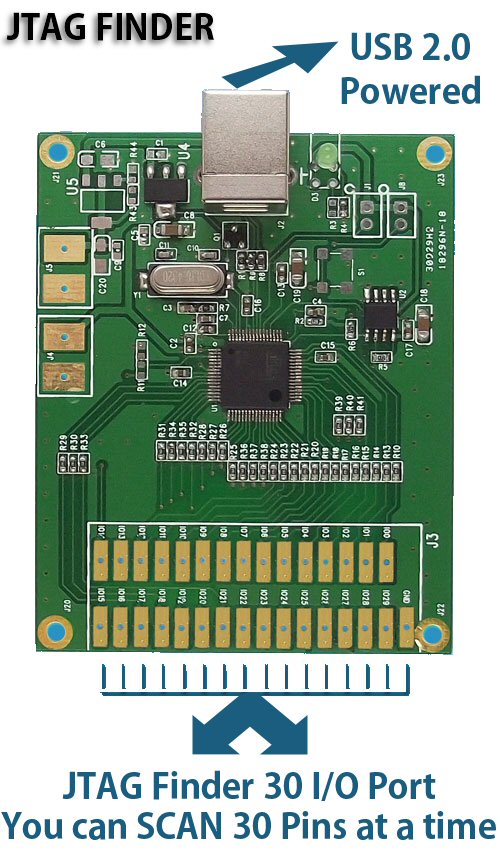
5 Steps Pinout Finding implemented
Step 1 - SRST
Step 2 - TCK / TMS / TDO Scanning with a single scan feature
Step 3 - TDI Pin
Step 4 - Scan TCK / RTCK
Step 5 - TRST
Downloads
JTAG Pinout Tool
Q: How many contacts on the card terminal can be analyzed?
A: The possibility of analyzing 18 contacts on your phone or modem card.
Q: Why 18 and not 30 or 40?
A: Because, in practice, more than half the vehicles on which a search pinouts were on average 7 – 10 possible points of contact, rarely come across machines with 10-12 points, 14 – is even rarer. Which accounted for a maximum of 16 points to scan it.
Q: Do all vehicles may find the pinout so?
A: No, not at all! There are terminals on which the conclusions of JTAG interface just is not divorced, or withdrawn, but are on the saw cut (end) board, where a connection to them is not possible. Also, there are literally terminals uniformly “studded” pads. Elucidation of pinouts on these terminals in this way is not a simple task with time-consuming. There are other difficulties, however, confident in most cases, pinout can be found.
Q: How long does the search procedure pinouts?
A: Time to search pinouts depends on two parameters. First – this is the duration of the preparation phase to the search. Depends on the complexity of construction of a concrete system and the design features of the board. The second is the duration of the search itself, which ranges from a few seconds with a minimum number of analyzed contacts (8) to about 8 minutes at the maximum number of analyzed contacts (18).
Q: What types of processors can work Search Pinout Tool Kit?
A: Search Pinout Tool Kit is designed for use with terminals processor-based company Qualcomm. Also it was used successfully on some processors, other companies (Intel, VIA, Broadcomm, Atmel).
Q: Is there a possibility Updates Search Pinout Tool Kit and will they be paid?
A: Updates client software and firmware of the controller associated with the removal of bugs and adding new features will be free.

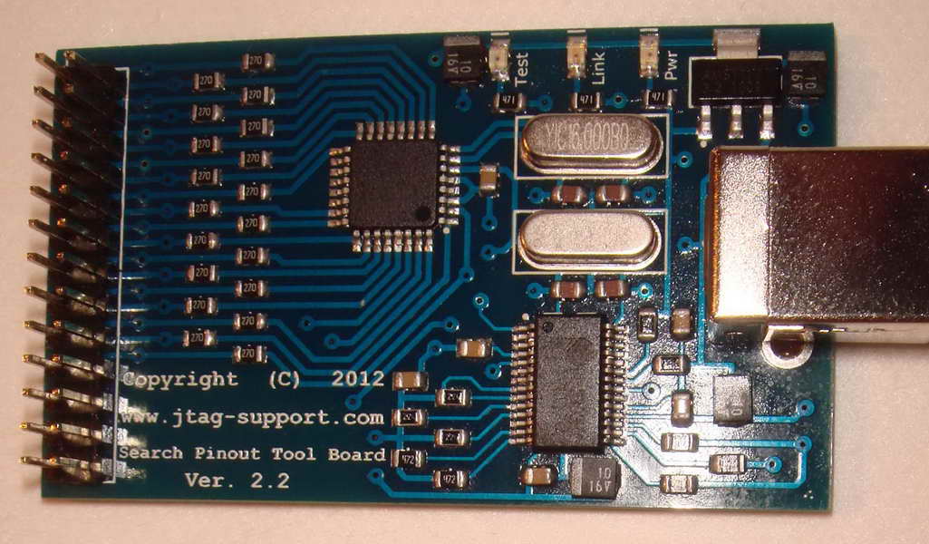
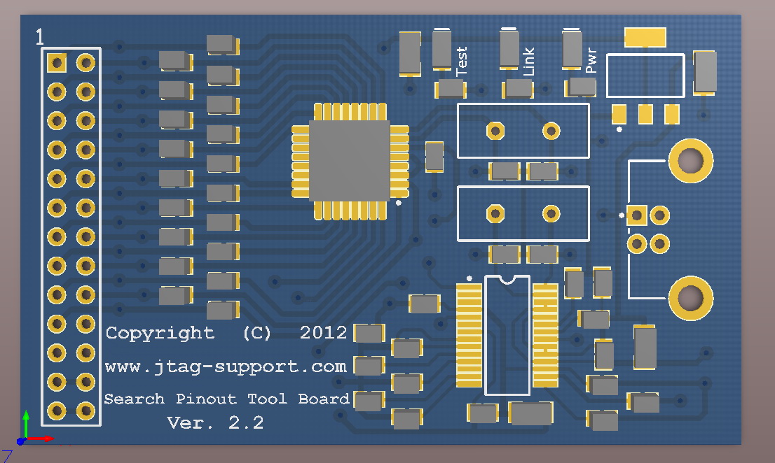
Three Simple Step.
1. Disassemble the phone. Determine the likely pinouts of JTAG on the board or on the socket. A schematic sketch them on paper. Check the possible presence or absence of the necessary bridges. Remove unnecessary or close the necessary bridge.Connect the phone board and SPT Board via GNDwire.
2. Connect the SPT Board with a computer. Connect phone board to a power source. Turn on the phone, preferably in Emergency. Using the output TEST SPT Board in turns touching each of the proposed findings with the JTAG watching the behavior of the device. If phone consumption is dropped, which means either reset the device, or it off, note the output on paper and remove it from the “Search group”.
3. Except from the “Search group” all “critical” pads (ps_hold, reset) soldered in turn to the remaining pins of SPT Board beginning with the first order. Make sure the unit is turned on, you can start your search.
If the “Search group” contain JTAG pins: TCK, TMS, TDO, TDI, TRST. Search Pinout Tool Kit will determine which of the conclusions phone board represent with pins SPT Board. It also considers the processor ID CODE connected device. Based on the correspondence be noted on paper pin assignmentJTAG.
Latest version Client Programm
Microsoft Framework Download Link
USB to SERIAL Driver
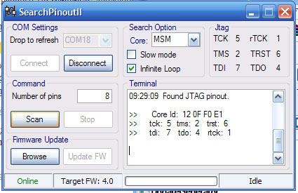
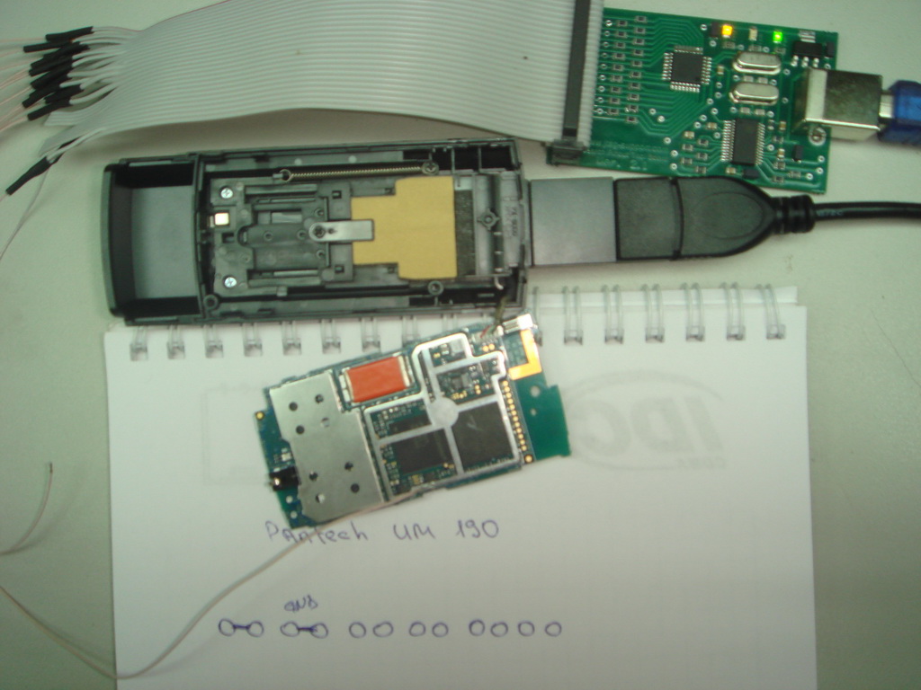
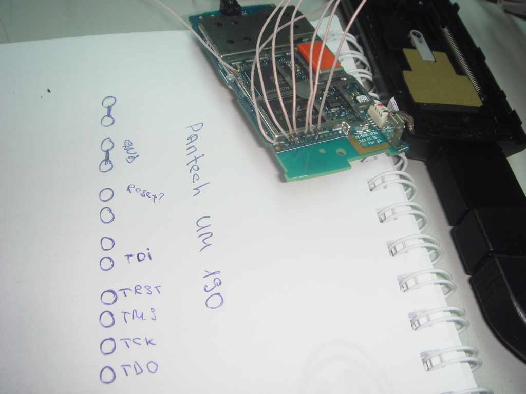
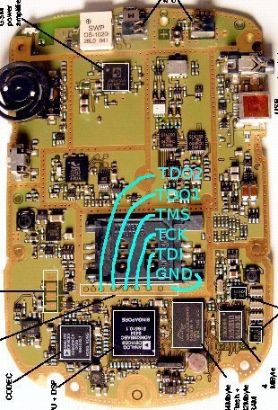
Search pinouts for PANTECH UM190 modem
On opening the modem is easy to detect a fairly large number of contact pads.
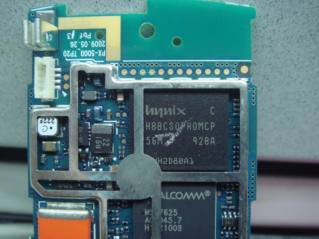
Appearance modem board
Looking closely to them at once can be dropped four of them, the two joined together and the two are connected to “ground”.
Schematically sketched the location of contacts
Turn on the modem we explain the presence of findings ps_hold and or reset. When you tap a contact terminal TEST restarts the modem.
Determining the ps_hold and reset method of "spear"
In this case, the modem reboots when you touch just one output, usually two.
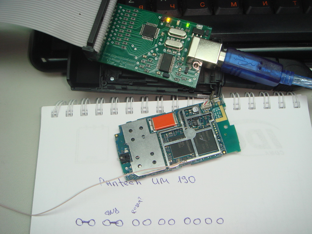
Marked on the paper output resets the modem
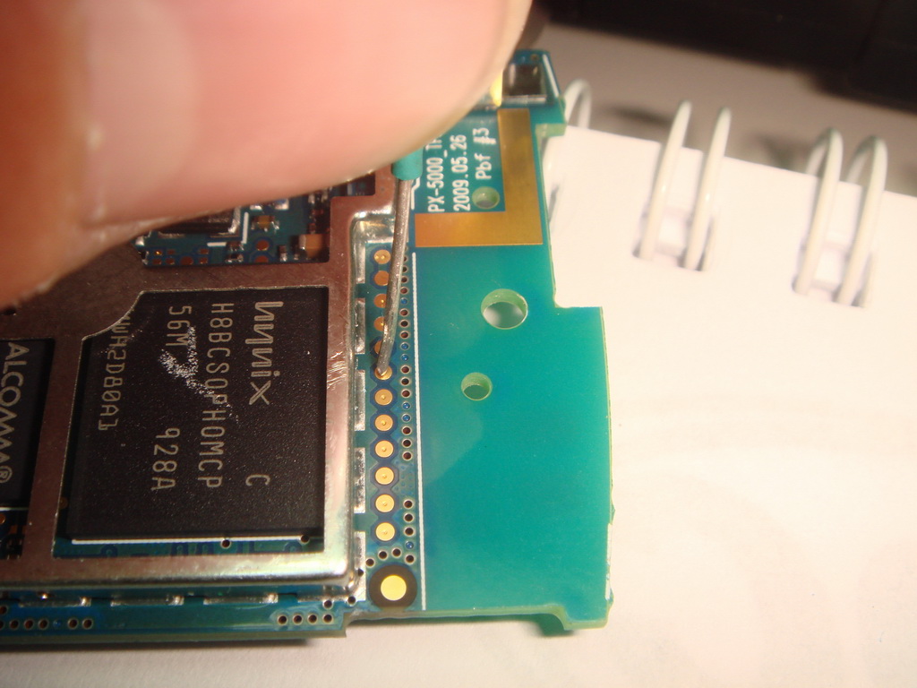
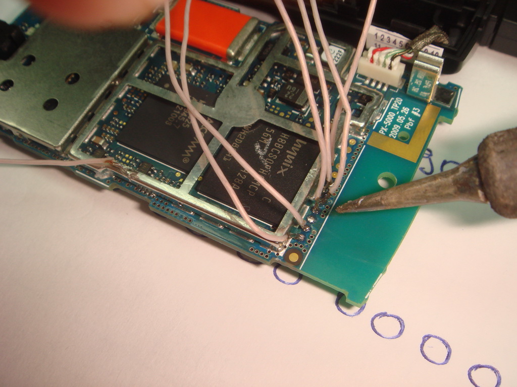
You can now soldered to the remaining contacts modem and start auto search.
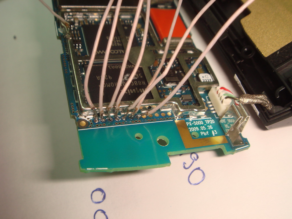
soldered pads
Trying to find pinout when the modem was not successful. Most likely a modem software disables theJTAG interface, so you should try to find pinout before the modem firmware will disable the JTAG.
At the time of withdrawal and the power supply to the modem client program can generate false detection alert pinouts, it is normal in mind the conclusions of the instability of states at the moment when the modem. In this case, false messages look like this:
False pinout at the time of power off
False pinout at the time of power on
The number of false piouts may vary in this case, there were about 4-5.
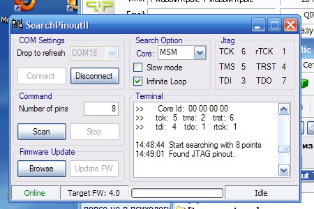
While the modem continues to load, and at this point is the detection of the correct pinouts, as judged by read by the CPU ID CODE.
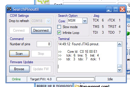
Correct pinout defined at boot time the modem
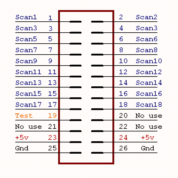
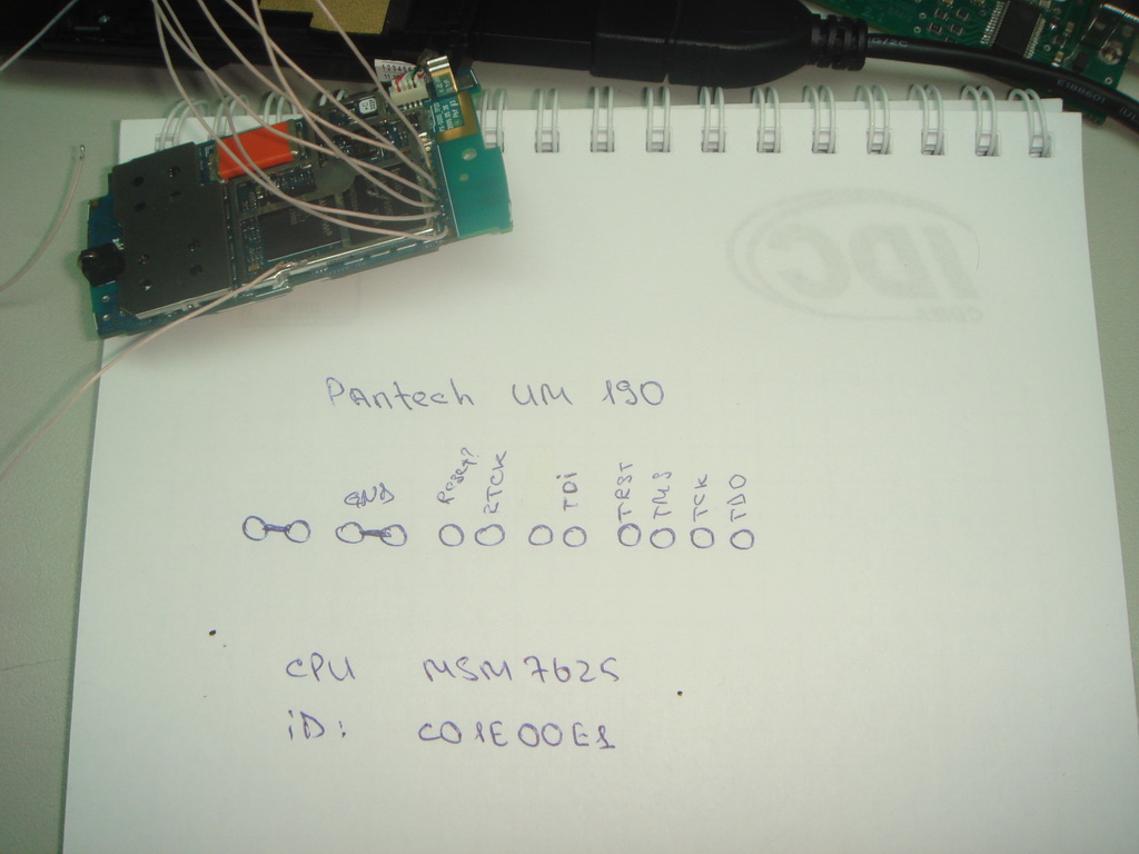
Marked on the diagram pinout. All pins except RTCK
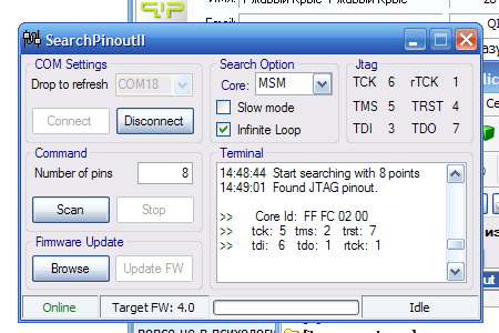
Sketched the location of the findings can be confirmed whether the output device found RTCK or number 1 was assigned to him by default. To do so, resolder SPT Board findings to the modem so that the number corresponding to the output pin TDO was the maximum (in our case it was and is the seventh number of the seven involved findings), and display a contact number for this RTCK was greater than 1.
Swap 1 and 5 output
Start the cycle search again and make sure that the contact number RTCK correctly determined.

Correct pinout including contact RTCK
Note the remaining data in the paper. Work to determine the pinouts over.
JTAG Pin Finder
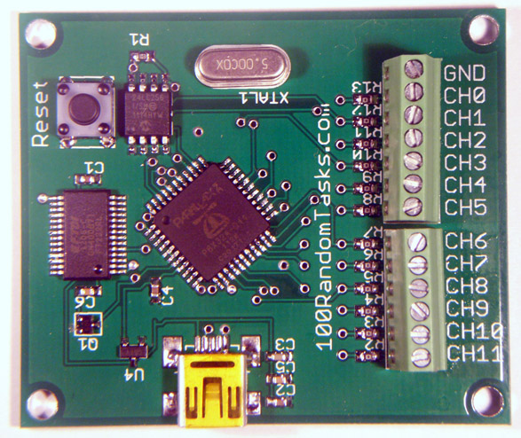
Update: We are now currently selling the JTAG Pin Finder.
Click here for details. ::: Now selling the JTAG Pin Finder.
Recently I was contacted by a Detective from the Victoria Police -
Forensics Department inquiring if I knew a way to determine the TAP pins on cell phones
when the pins are not labeled.
Upon giving it some thought, and researching the particulars of the JTAG protocol,
I determined that it would be possible to some extent.
So I began putting a prototype board together,
and with the use of two Samsung phones the Detective sent me, I started to it.
The hardware is decidedly simple.
I used a Parallax Propeller microcontroller connected to an FT232 USB to Serial converter and a USB mini connector.
I chose the Propeller because of its easy programming and debugging through the USB as well as
the fact that it has 28 free pins for interfacing.
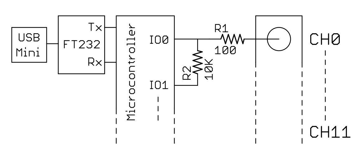
The interface to the cell phones is nothing more than 100 ohm resistors in series with the pins
under test for current limiting purposes.
In addition, a 10K resistor is connected from each channel pin to a free IO pin.
This allows the unused channel pins to be pulled either high or low independently.
As the sniffer has 12 channels, 24 IO pins are used along with 2 for the UART,
and 2 for the 32K EEPROM for a total of 28 used pins and 4 free pins left over.
This particular setup is easily implemented on any microcontroller with enough free pins.
The software is the heart of the unit. At its core is the combination array used for testing. I spent some time researching combinatorics and looking unsuccessfully for an algorithm to generate the possible combinations. I found many websites that described the total number of combinations possible, and in my case, I needed the number of 4 line combinations of a possible 12 lines with the order being important. This total was 11880 possible combinations. I did find a website (link here) that listed all the combinations for me and had a handy option to save this as a file. All that was left to do was to write a small VisualBasic.NET program to parse the file and save the data in a binary format usable by the Propeller. Since I have 12 channels, each combination item would fit into a nibble. As such, each combination consumed 2 bytes of memory, and since there are 11880 combinations, a total of 23,760 bytes were needed to store all the possible combinations on the Propeller. So for the first combination (0,1,2,3) – Byte 0 = 0x01, Byte 1 = 0x23. This is why I chose 12 lines and not more. As you add more lines, the possible combinations grow exponentially. For example: 13 lines – 17160, 14 lines – 24024, 15 lines – 32760, 16 lines – 43680. Since the Propeller has 32K ram on board, memory for 12 lines is the most it could hold directly.
The basic operation of the firmware is as follows:
- Load the first combination from memory
- Set the TCK, TMS, TDI channel pins to output and the TDO pin as input as specified by the loaded combination.
- Set all channel 10K resistors to pullup so as to prevent floating pins.
- Reset the device TAP.
- Scan for possible devices. If no devices are detected, load the next combination.
- If the ID command is known, send the ID command to the device and read back the ID code.
- If the ID command is not known, reset the device and move directly to the Shift-DR state and read the ID code.
- If the ID code is equal to 0xFFFFFFFF or 0x00000000, discard the combination and load the next combination.
- If a possibly valid code is found and the ID command is known, reread the ID code directly after a reset and
confirm that the codes match. If they do not match, discard combination and load the next combination.
If they do match, save the combination and ID code.
- If a possibly valid code is found and the ID command is not known, save the combination and ID code to be listed after
all combinations have been tried.
- Once all combinations have been tried, list all the possible combinations.
The particulars of moving to and from various TAP states can be found quite readily online, so I won't go into the specifics of TAP control or basic JTAG operations here.
One additional feature that was added to the firmware is to enter the number of unknown channels to use. By doing this, the firmware will skip any combinations that include any channels that are not used. This will speed up the search process depending on the number of channels used.
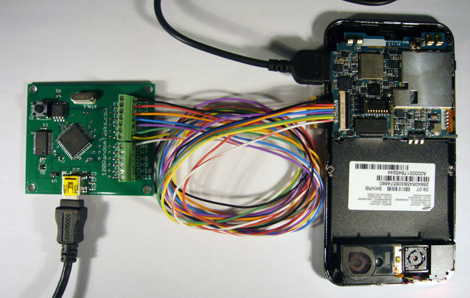
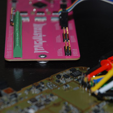
The JTAG Pin Finder connected to one of the Samsung phones send to me by the Detective.
The JTAG portion focuses on the ID word contained in the device.The ID command is optional according to the IEEE 1149.1 spec but most if not all manufacturers implement the command. After resetting the TAP, the ID code is automatically loaded into the Data Register. If you move the TAP to the Shift-DR state, you can clock out the ID code.
This is how the firmware searches for possible combinations without using the Instruction Register. The disadvantage to this method, is that it will likely result in multiple combinations being found. However, by inspecting the found combinations, you can deduce what pins to focus on. If you look at the image on the right, you will see that the firmware found 6 possible combinations. This is on the phone shown above. You can see that the TCK and TDO pins are identical on all combinations, and the TMS is the same for 3 of the 6 combinations which would be a good guess that it is the correct pin. Finally, The TDI pin is channels 0, 4, or 6. So from being completely in the dark with an unknown header, the firmware has reduced the options to just 3.
This is the search option for an unknown device, scroll down to the next section to see how the firmware resolves a known device.

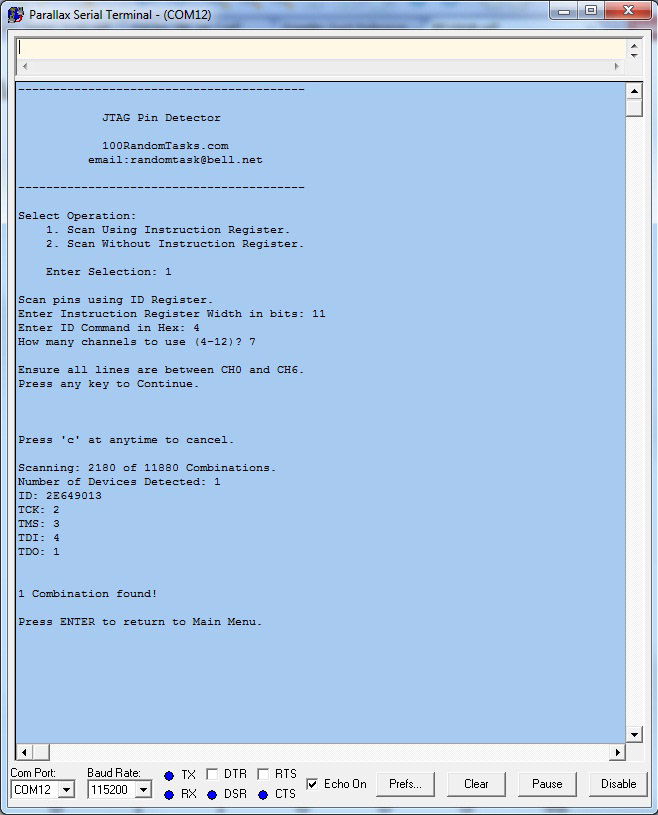
The best way to find the unknown pins is with the use of the ID command. To search this way, the firmware needs to know two things: The length of the Instruction Register, and the ID command value. Both of these can be found in the Boundary Scan Description Language file, or BSDL file. In addition to these two requirements, the BSDL file will also contain the ID code value. This is great because it adds another level of confidence when the firmware finds a valid combination.
In the example on the right, the Samsung SCH-i910 phone uses the PXA312 processor. After a short search online, the BSDL file specifies an Instruction Register width of 11 bits, an ID command of 0x04, and an ID code of 0x2E649013.
Plugging the two requirements into the software and starting a search resulted in the combination shown to the right. As you can see the ID code is exact, and there was only one valid combination found, which is also correct.
I have tested it with the other phone the Detective sent me, which happens to be another Samsung model with a different processor, with similar results as shown here.
Now selling the JTAG Pin Finder.
- Searches can be of one of two ways:
- Using the Instruction register (Inputting the IR width and the IDCODE command) and usually results in a single match.
- Without the Instruction register (Results in several matches from thousands
which can then be tried individually for the correct combination).
This device has been sold to several law enforcement agencies to assist their electronics crime labs
in determining the JTAG pins of primarily cell phones.
JTAG pinout detector
This code can be used in combination with an Arduino Mega in order to detect the JTAG pinout of your prefered electronic device.
Code modified from EnumJTAG and Arduinull:
http://hackerspace.be/images/4/48/Serjtar_table.pde.txt
Arduino Mega at 3.3v
- Use the arduino mega pins 22-43
- jtag TAP reset before every try
- output in tab-separated table
- Your arduino mega should run at 3.3v, for example, by using a hacked USB cable,
which forks the 5v power from the USB to inject it into the external power connector

- http://deadhacker.com/2010/02/03/jtag-enumeration/
- http://lekernel.net/blog/?p=319
- http://hsb.wikidot.com/arduino-jtag-finder-workshop
JTAG Finder

Atmel AVR based JTAG scanner
JTAG is a standard for device testing ports found on the PCBs of many devices.
Finding the pads and pinouts for these ports allows hackers to gain access to the embedded systems,
their on-board debugging tools, etc., effectively providing a back door.
But determining the JTAG pinouts can be a time-consuming and frustrating process.
To help in this, a German hardware hacker named Hunz has created the JTAG Finder,
an automatic JTAG pin-out detector, using an 8bit AVR ATmega16/32L microcontroller.
Details of the project, and a call for others to get involved, can be found on the JTAG Finder wiki.
He also wants to build a JTAG Found database of known device pinouts.
Related:
JTAG Finder
User:Hunz is searching a maintainer for this project! Since he currently doesn't have the time/will to realize the further plans.
Due to his talk held at the ph-neutral, this article is undergoing a major rework.
(How) Does this work?
- The slides from my talk at ph-neutral 0x7d6 are here odp.
(hunz.org seems dead so pdf version now uploaded to elinux, enjoy)
- It did work with
- my fpga board (2 chips in one test chain) from http://www.fpga-dev.de
- the blackberry from the slides
- It didn't work with
- a grandstream SIP phone yet (maybe some (n)TRST) problem or JTAG disabled
- some kind of D-Link VPN gateway? (didn't ask for the exact name)
What does it look like?
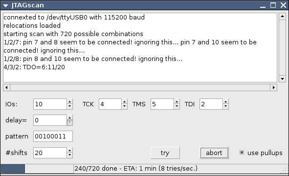
GTK GUI screenshot
Closer view at the jtagscan output for a blackberry
Further plans / What's missing?
Better methods
IDCODE
One should be able to reduce the number of necessary tries to (n * (n-1)) + (n-2) by reading the IDCODE from the Data Register:
Only TCK and TMS should be necessary for this, so one can look for TDO afterwards.
This method is described here: http://www.xilinx.com/xlnx/xil_ans_display.jsp?iLanguageID=1&iCountryID=1&getPagePath=11857
Possible problems:
- This doesn't work if a devices uses Bypass as default instruction, does it?
- One doesn't know the IDCODE in advance, thus detecting this pattern it is harder.
shift DR
shifting DR instead of IR might be faster? This is the case when the DR is smaller than IR.
The IDCODE must be 32 bits long, thus the DR register is 32 bits long if the IDCODE is loaded.
The IR length is usually about 36bits?
Better software
- retry on timeout
- live display for the status of each pin (at least while not scanning)
- IO entry field (to disable single pins or assign const values to them)
- (n)TRST support is missing (low active and with high active pulldown transistor)
- detect hi impedance pins by looking for pins that change their state with pullups (100k) on/off
- warn that hi impedance pins might be disconnected from the jtag!
- try the Hi + hi impedance pins for TMS, TCK, TDI first and
- the Low ones for nTRST first
- read IDCODE?
- assist the user in creating the relocations file (pullups on for all pins, user shall put cable between gnd and pin 1..30, one pin at a time)
Better hardware
- Arduino / Freeduino based hardware?
- Enable easy / fast deployment of the jtag finder
- USB connected or not (standalone) operation mode
- 1.8V support( needed for xbox 360 for example)
- AVR alone won't do here (except for tiny2313 but it doesn't have that much pins)
- thus I'm thinking about a cpld
- could use a whole gang of tiny2313's perhaps
- The current hardware is just a proof of concept. Let's build something fiddle-free.
- I'd like to design a circuit board for this - if you want one as well please add yourself to this list:
- Hunz
- Obsidian
- Let's collect some suggestions for the hardware here as well. My current suggestion is:
- USB powered, USB-to-Serial interface (115200 baud)
- socket for an ATMega16L or 32L? running at 7.3728 MHz (for the 115200 baud)
- DIL or SMD? (TODO: compare the costs)
- Obsidian: Wouldn't DIL make it easier for people to build their own boards?
- bootloader for firmware updates
- floppy connector compatible 2x17 pin header for the cable to the testpins
- extra STK500 compatible pinheaders (maybe unpopulated) without the 330 Ohm resistors for other applications
- costs: about 15-20 Euros
- PLEASE add your comments/suggestions!
- are 30 IOs enough or do you want more?
- Certainly sounds enough for me for the first design.
- the ATmega16/32 got 1/2kbyte of SRAM - it's enough for the JTAG scanner but maybe you'd like to do some other things with the board as well?
- do you want more processing power? again it's enough for the JTAG scanner but one might want to do other things which need more processing power
- or would you prefer to keep it simple, stupid?
- are 30 IOs enough or do you want more?
Better firmware (AVR)
- assembler for the scanning function -> speedup
- TX buffer, interrupt based TX while doing sth. other
- full duplex for uart? scan new pair while TX for old one running?
- TX only interesting pins?
- access the current TCK/TMS/TDI lines via RAM (ld/st) instead of IO (in/out) -> no case/if needed - just add the port offset
- better delay
- shift TMS/TDI, read TDO support - to use it as openwince-jtag cable
- autonomous scanning?
- 7.x MHz support
The Hardware
Explanations
not much to explain - had an ATmega32 lying around...
The Software
- the current sourcecode is here: jtagscan.tar.bz2
Explanations
- there's a file named relocations.avr
- it maps floppy connector / cable pin number to AVR port/pin
- AVR port A = 0, B = 1, C = 2, D = 3
- each AVR port got 8 pins
- first line in the relocations file is pin 1, 2nd is pin 2, etc.
- if there's a 13 in line 5 it means: cable pin 5 = avr port 13/8 (=1 = port B), AVR pin 13 mod 8 = pin 5
- use pullups
- should be useful for nearly any device to avoid thrashing input lines
- disabling it leads to false positives
- delay
- currently (1.8MHz), 0 is safe (about 100kHz)
- higher values will slow down the scanning process
- shift pattern
- you can leave this alone
- # shifts
- often you can reduce this to speed up the scanning process
- number of times the 8bit-pattern is shifted into current TDI pin
- so the number of bits shifted is #shifts * 8
- detection fails if the value is too small - retry with a bigger value if necessary
- 15 should be ok for most devices
Output
- 4/3/2: TDO=6:11/20 means:
- for TCK pin 4,
- TMS pin 3,
- TDI pin 2,
- pin 6 ist a TDO suspect - the pattern was shifted in 20 times in at pin 2 (TDI) and found 11 times at pin 6
- more advanced: output while scanning a blackberry 7290
- scroll upwards and use the gallery
If it doesn't work
- have you tried a higher number of shifts?
- have you tried increasing the delay?
- have you run the scan a 2nd and a 3rd time?
- nTRST might be pulled low - the current software doesn't yet support this
- enhance the software ;) (ask me if you need help - scroll down for contact)
JTAG might be disabled
- by removing some 0-Ohm resistors on the circuit board (look for a connection to the testpins at missing resistors)
- by adding additional resistors to set pins to a constant value
- if you can't pullup/down a pin with 330 Ohm it's either Vcc/GND or disabled using this method
- look for a connected resistor and try removing it
- by a burned fuse directly in the chip
- bad luck for mortals like us ;-(
- by software
- maybe keeping the cpu in reset state might help?
Comment from user of many JTAG tools
I think this tool can be quite dangerous when used on some JTAG ports, if you look at [1], for example MPC BDM port (also usable as a JTAG connection) is bad one. If the port has only TCK/TDO/TMS/TDI/nTRST/nSRST pins, then nothing wrong *should* happen, but if there are other signals, be very careful.
Also if you just try random IR/DR scans on a JTAG-enabled chip you may destroy it. For example some CPLDs have special IR command that erases internal flash memory, but this command requires clocking and some termination. When run improperly it can destroy the flash.
- http://en.wikipedia.org/wiki/JTAG
- The jrev tool by Stanislaw Skowronek tries to automate the process of reverse-engineering the board connectivity.
- http://www.asset-intertech.com/products/free_resources.htm - various resources
- http://www.openjtag.net/wiki/
- Common JTAG Pinouts
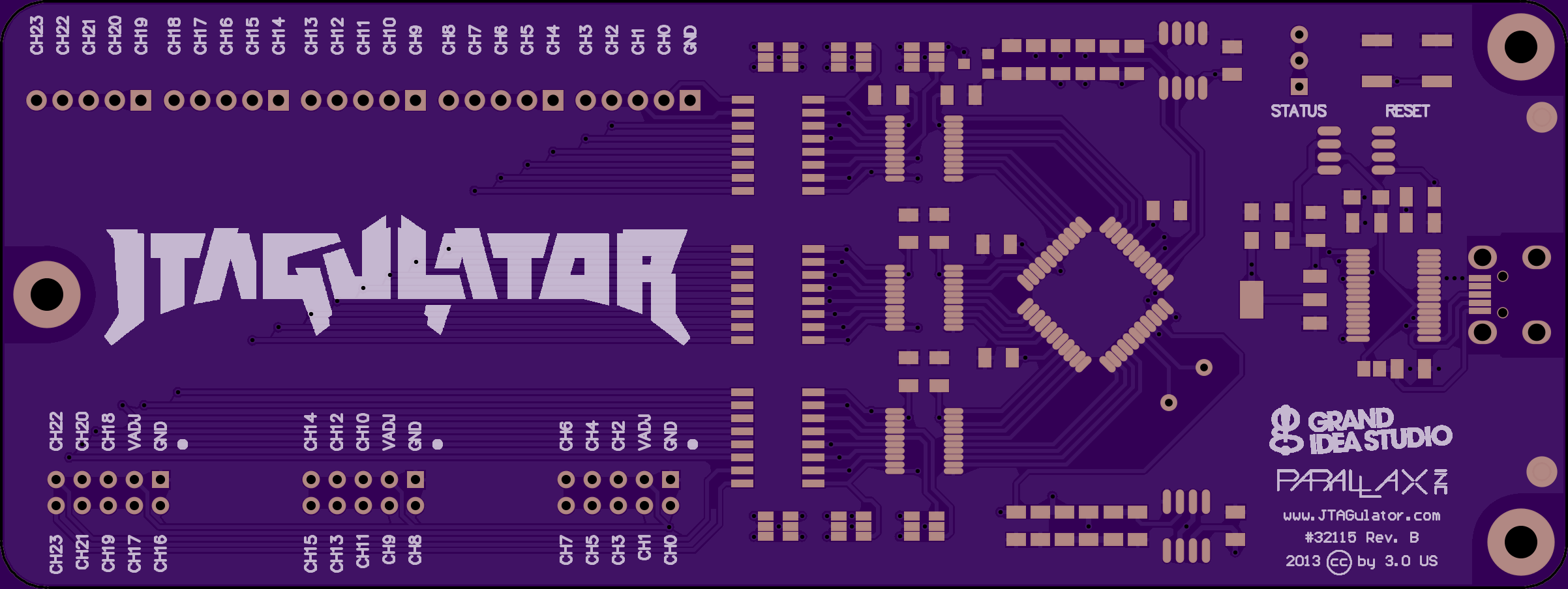
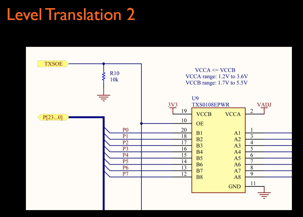
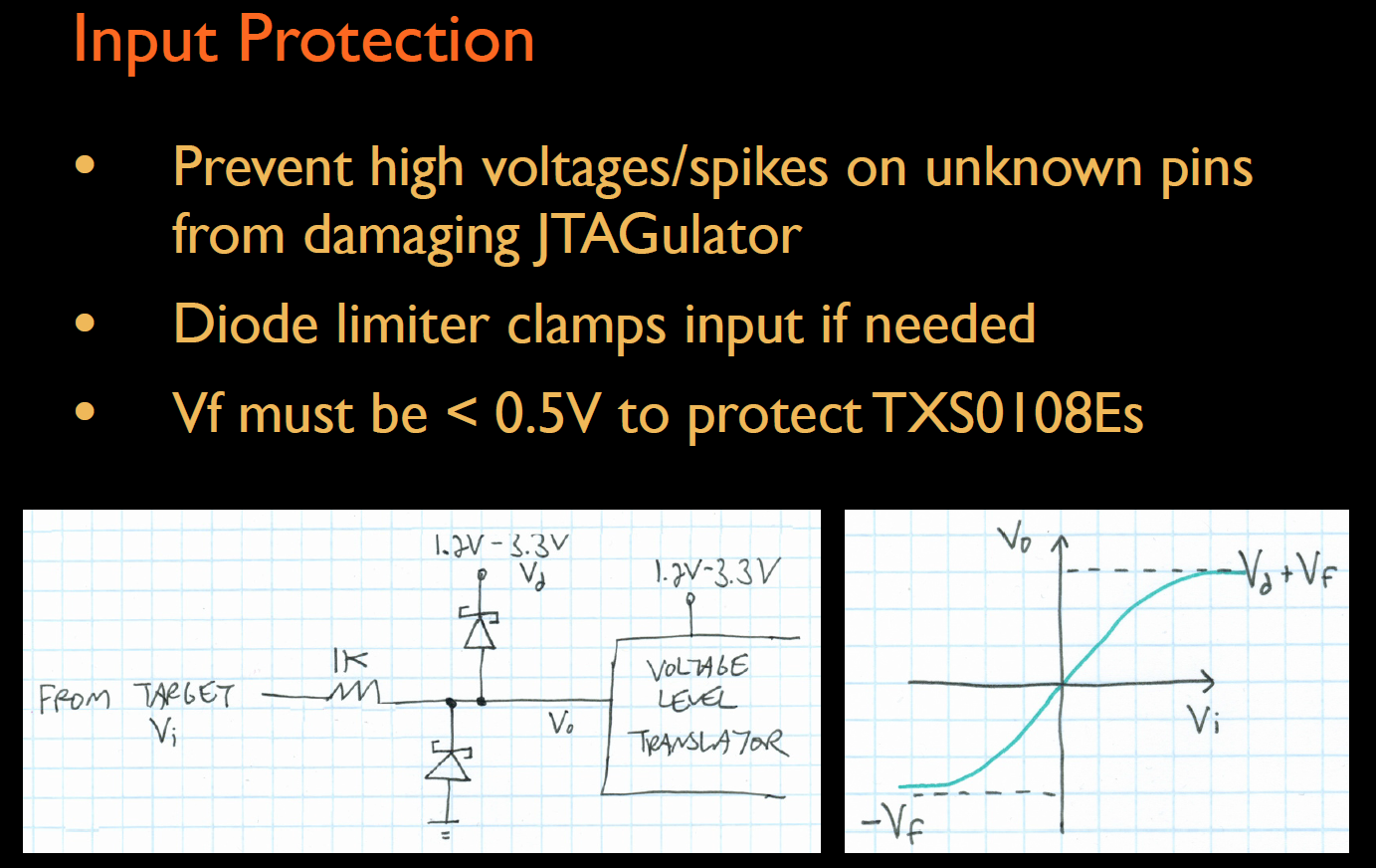
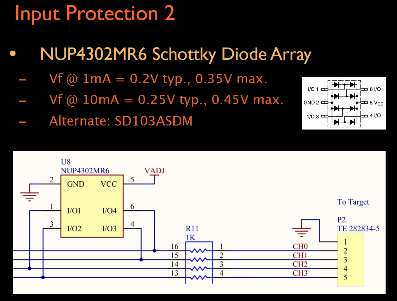
JTAGULATOR http://www.jtagulator.com


On-chip debug (OCD) interfaces can provide chip-level control of a target device and are a primary vector
used by engineers, researchers, and hackers to extract program code or data, modify memory contents,
or affect device operation on-the-fly.
Depending on the complexity of the target device, manually locating available OCD connections
can be a difficult and time consuming task, sometimes requiring physical destruction or modification of the device.
JTAGulator is an open source hardware tool that assists in identifying OCD connections
from test points, vias, or component pads on a target device.
Assembled JTAGulators are available from Parallax, Inc.
For questions and technical support, please contactsupport@parallax.com.
This design is distributed under a Creative Commons Attribution-3.0 United States license.
The JTAGulator name and logo are registered trademarks of Grand Idea Studio, Inc.
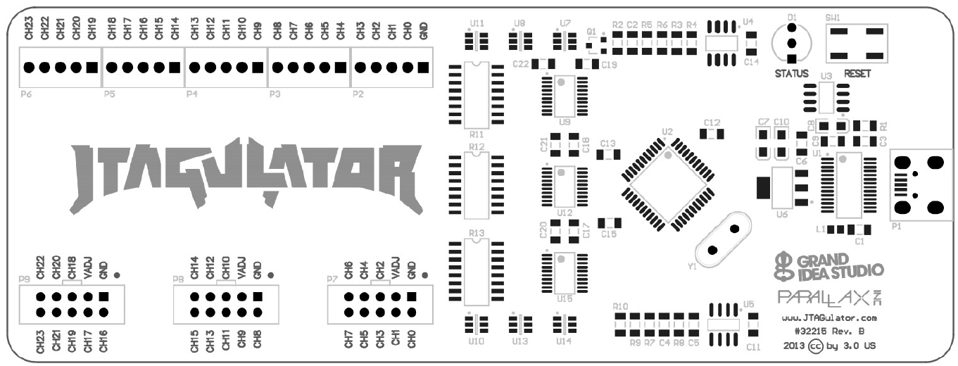
MODULE HIGHLIGHTS:
- 24 I/O channels with input protection circuitry
- Adjustable target voltage for level translation: 1.2V to 3.3V
- Supported target interfaces: JTAG/IEEE 1149.1, UART/asynchronous serial
- USB interface for direct connection to host computer
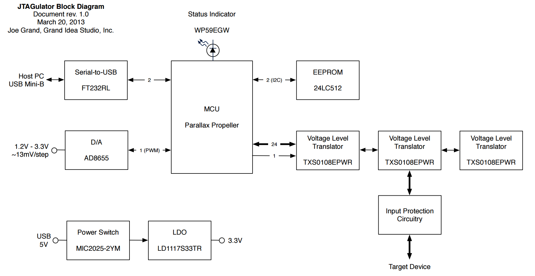
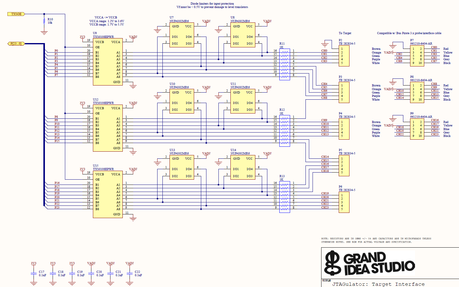
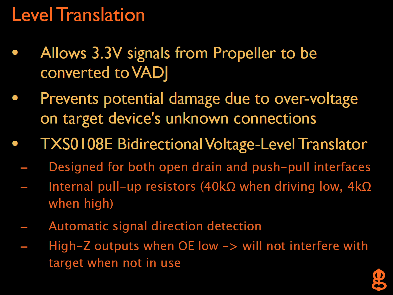
DOCUMENTATION:
- Product Brief (from Parallax)
- Block Diagram
- Schematic
- Bill-of-Materials
- Assembly Drawing
- Gerber Plots
- Test Procedure
- Source Code: Parallax Propeller (GitHub)
ADDITIONAL RESOURCES:
- Slides: JTAGulator: Assisted discovery of on-chip debug interfaces
- Video: Introduction and Demonstration (Expanded) (YouTube)
- Video: Updating Firmware (YouTube)
- Video: Black Hat Asia 2014: JTAGulator Part 1 andPart 2 (YouTube)
- PCB rev B. on OSH Park
- Poem by Zach Houston
JTAGulator Product Brief


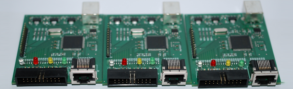
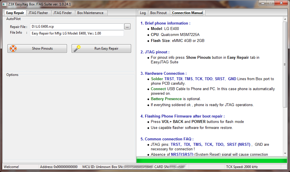
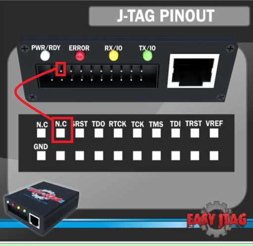
Z3X Easy-JTAG
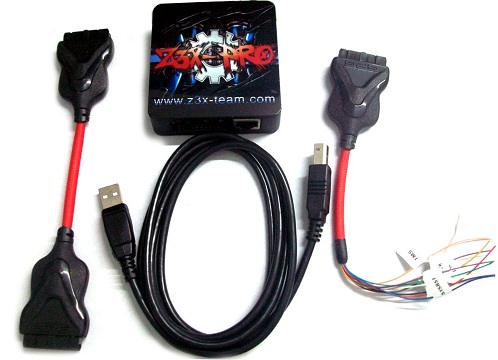

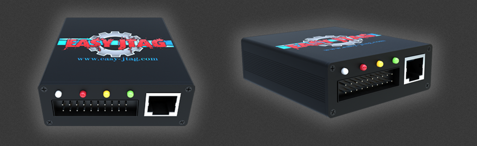
This product is a result of 4 year developers’ own solutions which makes it the most reliable servicing tool on the market
EasyJTAG Box is a professional JTAG programmer allowing you to work with devices
(single or united into common chain) through JTAG interface.The main intended purpose of
EasyJTAG Box is repairing dead boots of the devices (routers, aricards, smartphones, PDAs, modems, mp3 players, etc.) or
these devices recovery until they become fully operational. EasyJTAG Software is Windows
application for EasyJTAG Box providing fast and easy interface for devices recovery.
- Easy-JTAG have unique function hardware JTAG-FINDER.
- Easy-JTAG have possibility activate any known N1 z3x box sofware.

Forum : Easy-Jtag
Supported Chipsets and Cores for JTAG I/O operations:
- Generic ARM Cores: ARM7TDMI, ARM9 (ARM920T, ARM926EJS, ARM946, ARM966), ARM1136EJ, ARM1176, CORTEX-A8, CORTEX-A9;
- Qualcomm QSC Family: QSC1100, QSC1110, QSC6010, QSC6020, QSC6030, QSC6055, QSC6085, QSC6240, QSC6270;
- Qualcomm MSM Family: MSM6000, MSM6150, MSM6245, MSM6246, MSM6250, MSM6250A, MSM6260, MSM6275, MSM6280, MSM6280A, MSM6281, MSM6800A, MSM6801A, MSM6290, MSM7200, MSM7200A MSM7201A, MSM7201, MSM7225, MSM7227, MSM7625, MSM7627, MSM7230, MSM8255, MSM8255T, MSM8260, MSM8960, APQ8060;
- Qualcomm QSD Family: QSD8250, QSD8650;
- Marvell/XScale Family: PXA270, PXA271, PXA272, PXA310, PXA312, PXA320;
- Samsung Processors: s3c6410, S5P6422, S5PV310,S5PC110, S5PC210;
- OMAP Family: OMAP1710, OMAP3430, OMAP3630, OMAP4430;
Following features supported by current Easy-Jtag core firmware 1.44:
- ARM7/ARM9/ARM11, CORTEX-A8, Cortex-A9 Dual cores support;
- Multiple devices on JTAG chain are supported, thus TAP number selection is available;
- Any custom voltage level selection from range ~1.8V to 3.8V (VTREF pin is not required for connection)
- Custom TCK Speed presetting slection from range 100kHz to 12000kHz
- TCK/Adaptive clocking selection
- Halt core (NRST is not changed)
- Reset core (NRST is applied before halt)
- Direct Read and Write memory (by 8/16/32-bit mode or bulk transfers)
- Access to the control registers of ARM core (coprocessor 15)
- Program code breakpoints
- Run Halt Restart core
- 19 Pins Hardware Accselerated unique finder feature offered only by Easy- JTAG
- NAND/ONENAND/EMMC/NOR DCC Read/Write/Erase operations
- NAND/ONENAND Read Spare, Write Spare, ECC support
- Multiple flash chips (address space) support
- NAND bad block management options: cancel, skip and ignore
- Easy Jtag One Button repair, resurection help and interface pinout for each supported model
Easy -JTAG PINFINDER specification:
Easy-JTAG Pinfinder is an unique hardware feature of Easy-JTAG BOX that helps find JTAG pins in
Sony Ericsson, Samsung, Chinese Mobiles, Huawei, ZTE, Alcatel and other CDMA and GSM phones.
EasyJTAG Pinfinder allows you to benefit from EasyJTAG Suite software as well.
Features of Easy-JTAG Box Hardware Pinfinder :
- UltraFast pinout detection algorithm ( fastest in the market )
- Multi TAP detection support ( up to 3 TAP's in scan chain )
- No need any user iteration for finding main JTAG pins.
- Detection of main jtag pins ( TCK , TMS , TDO , TDI and TRST )
- Allow manual pinout selection and correction rom GUI
- Allow save and restore found pinouts in profiles.
- Easy-JTAG Box Pinfinder - Technical Details
- Technology: Ultrafast FPGA JTAG Mux ( JSpider™ technology )
- Dynamic JTAG lines : TDI TDO TMS TCK TRST SRST
- Static JTAG lines : GND ( wired on 20th pin of JTAG header )
- Maximal finder pin count : 19 ( can be extended to 26 with RJ45 port )
- Maximal time for detection pinouts : 15s
- Minimal IO voltage : 1.8
- Minimal IO voltage : 3.6
- Regular firmware updates.
Easy-JTAG Box Pinfinder - Supported ( Tested ) MCU’s:
- Generic ARM Cores: ARM7, ARM9 (ARM920, ARM926, ARM946), ARM11, CORTEX-A8,CORTEX-A9;
- Qualcomm QSC Family: QSC1100, QSC1110, QSC6010, QSC6020, QSC6030, QSC6055,QSC6085, QSC6240, QSC6270;
- Qualcomm MSM Family: MSM6000, MSM6150, MSM6245, MSM6246, MSM6250, MSM6250A, MSM6260, MSM6275, MSM6280, MSM6280A,
MSM6281, MSM6800A, MSM6801A, MSM6290, MSM7200, MSM7200A MSM7201A, MSM7201, MSM7225, MSM7227, MSM7625, MSM7627, MSM7230, MSM8255, MSM8255T, MSM8260, MSM8960, APQ8060;
- Marvell/XScale Family: PXA270, PXA271, PXA272, PXA310, PXA312, PXA320;
- Samsung Processors: S5P6422, S5PV310,S5PC110,S5PC210;
- Possible more other cores. We need testers!
Supported mobile phones and modems brands: Samsung, LG, Zte, Huawei, Sony, AMOI, BENQ, Motorola, HTC, GSMART, Sierra Wireless,
Supported phones by one click button: at this moment after 4year of research list of phone is very lage, more than 300 devices,
last monthes we got thousands emails with date or release this unique device. So we decide release this asap with most wanted
phones, in next few weeks will be added much more resurectors, with high quality pinout pictures and good manuals. Our designer work
10h every day for this .
Easy-Jtag Box Hardware specification:
- USB 2.0 High Speed Buffered Interface:
We use an native USB Stack. Upstream data are directly arrives to box MCU without getting slowed by
bottleneck technologies like Prolific or FTDI chips. CDC Stack are give enough performance to match high load aplications.
- Native USB CCID Smart Card Reader:
Security are very important part of all GSM software project.
We use military standart GEMALTO Security for most our software.
Box has such card reader avaiable to software in native way. Box are fully capable with previous Z3X box based on FTDI and Alcor logics. It use same card and same software.
Its amazing , You can install your existing security card in box and get perfect 3-in-1 magic solution
- Super Speed Xilinx FPGA Driven Core:
Field-programmable gate arrays (FPGAs) are devices that contain programmable logic and interconnects.
Incorporating FPGAs into the design of Z3X jtag box ensures that users are able to program or configure boards
to erform basic logic gate functions such as AND and/or XOR, as well as, more complex combinational functions such as decoders bus controllers and pinout searching logic.
- ARM20 Industry Standard JTAG Port:
The 20-pin connector is the currently recommended from ARM. You can use different adaptes and jigs ,
available on market without need soldering or paying for additional converters Connector type: 20-way IDC male eader, 0.1” pitch. Use any 20pin Jtag connectors or jics! Easy and Universal!
- RJ45 MultiPort UFS3/Unibox Capable:
Box are equipped with classical RJ45 Unibox connector. You will be surprised ;-)
You can plug any type of cables UFS and Unibox. Box will automatically reconfigure power and data lines align.
Box are configured as standard unibox after powerup and switch mode after starting corresponding software. Easy and Universal..
- Integrated ADC and DAC for voltage control:
You can flexibly adjust port IO voltage from 1.8 to 30 volt. Also box can easy measure internal and external voltage with high precision. Easy and Flexible! You can monitor VFEF line of your device in realtime to be shure that all powering
on before connection.
- Integrated surge and overvoltage protection:
Connection errors ? Bad cables ? What else can break high cost equipment or PC motherboard We integrated two level power control and protection subsystem to protect phone, box and your PC You can be shure that even you plug in box ports an spoon everything will be protected from disaster.
Easy and Safe!
==================================
When you buy Easy-JTAG Box , you get: JTAG hardware box + z3x card(inside box )+ jtag activation(inside card) and
FREE access to flash file download area at z3x-team.com
According this you can many options:
1. For existed z3x user(with gemalto top cards) possible buy only JTAG hardware + activation, as they can use z3x cards inside jtag,
price will be litle-bit cheap, but you will save space in table.
2. For new JTAG users, will exist possibility payed activating Samsung, LG or Sams+LG to JTAG box.
( result: best jtag + best samsung box + best lg box : 3in1 ).
Modif Easy JTAG
JTAG Enumeration
JTAGenum is an open source Arduino based hardware platform I built last year with three primary goals:
1. Given a large set of pins on a device determine which are JTAG lines
2. Enumerate the Instruction Register to find undocumented functionality
3. be easy to build and apply] (For a detailed discussion and tutorial video see here.)
The development of a device has various distinct stages handled by different people/companies that each assume the other has properly secured their part.
The security of devices often rely on obfuscation which makes it dificult for any part of the chain to evaluate the security of the whole.
This is a problem that JTAGenum helps address.
This was built for personal research and while working on various projects at Recurity Labs.
Please feel free to contact me with any questions, problems, targets or updates. I would be more than happy to share credit.
Related work:
There are two other tools for finding JTAG pins:
JTAGScan presented by Benedikt Heinz (hunz) at ph-neutral which inspired Arduinull by Sébastien Bourdeauducq (lekernel).
JTAGenum is most similar to the latter with the added feature of finding undocumented functionality.
Felix Domke (tmbinc) recently gave a lecture on enumarating undocumented JTAG instructions and anyone considering
using JTAGenum would do well to check his paper(cache)/lecture from the 26c3.
About JTAG
JTAG is a common hardware debugging interface.
It is used throughout the development chain of a device.
Layout designers and board manufactures that employ pick-and-place machines will use JTAG to test interconnectivity of components.
ASIC designers use it to test the internal state of the chips they build.
Software developers often use it to load firmware onto the device and to debug software.
For a varity of reasons JTAG is often left in the final product.
As such each stage of the development chain will attempt to obfuscate its existence or functionality.
ASIC manufactures often build in added functionality (such as logic analysis tools) and avoid mentioning
both extended and often basic functionality from their final documentation.
Layout designers might remove JTAG pins from the board, spread their contacts throughout on the board,
remove contacts and hide JTAG lines on inner layers of the board.
As mentioned before, this can make it difficult for any one part of the development chain to evaluate the security of the device as a whole.
If you are unfamiliar with the inner workings of JTAG skip to the A bit more about JTAG section for the basics.
Hardware
To use JTAGenum you need an arduino compatible microcontroller.
Arduino is a simple development enviornment (IDE) for various microcontrollers.
At the moment AVR and PIC variants are available and can be purchased anywhere from $10 to $50.
JTAGenum has been tested on
- the official Arduino Duemilanove,
- Arduino Mega (see hackerspace.be modifications),
- RBBB clone and
- Teensy++.
When picking your microcontroller platform consider two issues:
1. How many pins do you want to check on your target.
2. what voltage level does your target device require.
Concerning voltage most Arduinos work at 5 volts.
Some are switchable but even those that are not can be modified.
For example revision 1.0 of the Teensy++ with over 30 pins of i/o can be modified by hand to operate at 3.3 volts.
I show where to cut lines and install a voltage regulator over here (Update: Teensy++ version 2.0 has a spot on the pcb to install a 3.3v regulator).
For voltages other than 3.3v and 5v there are a variety of solutions that depend on if you need uni-directional or bi-directional support on your i/o lines.
Alessandro provides schematics and board/shield design for bi-direction i/o voltage conversion.
Finally, check your microcontroller on your Arduino board.
The Atmega328P supports a supply voltage of 1.8v to 5 so you could modify the board to support 1.8v.
In contrast, the AT90USB on the Teensy boards only support 2.4 to 5.
When connecting the microcontroller to the pins of your target one thing to be aware of is possible cross-talk between wires.
I’ve been using a patch cable from Amontec that has a lot of cross talk.
JTAGenum has a mode that helps check for this which I will get into more detail later.
Usage
Download the JTAGenum code and open it in the Arduino IDE.
The following needs to be changed in the code depending on your microcontroller:
- pins[] define which pins on the microcontroller are being used to connect to the target
- pinname[] is a convenient way to map the pins to names
which correspond to the names of pins on your target - IR_LEN defines the length of the JTAG instruction register.
If you change this you should also add ‘0’s to each of the coresponding IR_** instruction definitions.
You can find the IR_LEN in the documentation for your target.
If you cannot find it just guess. (10 is the current value, 8 is also common)
Upload the sketch to your microcontroller and open the serial console with a baud of 115200.
Sending a ‘h’ to the console will print usage information that describes each function.
Each function is enacted by sending the defined one character code:
v > verbose
Toggles verbose output. At times verbose might present too much information or without it too little.
l > loopback check
Find loopback pairs that will generate false-positives for other tests. After running you should remove any loopback pairs from your pins[]/pinnames[]. Looback pairs are found by sending a predetermined pattern[] to all possible pins while checking all pins for matching output. Because the JTAG clock (TCK) and state (TMS) pins are NOT being stimulated the input/output pairs where the pattern is found represent loopbacks. NOTE: you should probably run this once with and without internal pull-up resistors set (‘r’) to avoid problems of cross-talk which is discussed in detail later.
s > scan
This routine is used to check all possible pins and find JTAG clock, state, input and output pins lines (TCK,TMS,TDI,TDO). This is done by setting the JTAG state (TMS) into Shift_IR mode and then sending pattern[] to TDI and checking for it on TDO while clocking TCK. This check is run for every possible pin combination and it is important that you remove loopback pins before running. While this scan is meant to determine all of the JTAG pins required it is possible that the TMS pin found is incorrect. This depends on if the target uses the bypass register by default (described later). If an IDCODE register is present then bypass mode is not the default and you can assume that the pin this scan defines as TMS is correct. Otherwise, only the TCK, TDI and TDO pins can be determined. NOTE: run with pull-ups on (‘r’) as any cross-talk might result in false-positives.
y > brute force IR search
This will set the instruction register (IR) to all possible values and check the output. This can be used to find undocumented instructions and examine their results via the data register (DR). To run this scan you should have already determined the 4 JTAG pins and define pins[] as such: [0]=TCK [1]=TMS [2]=TDO [3]=TDI. NOTE: run with pull-ups on (‘r’) as any cross-talk might result in false-positives.
x > boundary scan
This will return the state of all the pins on the target. Actually it is not just the pins but the contents of the scan/sample register. This should be a rather large register and is defined in the code by SCAN_LEN+100. You can check your targets documentation and specify this or just leave it as a large number (currently 1800). To run this scan you should have already determined the 4 JTAG pins and define pins[] as such: [0]=TCK [1]=TMS [2]=TDO [3]=TDI. NOTE: run with pull-ups on (‘r’) as any cross-talk might result in false-positives.
i > idcode scan
The JTAG standards specify that if an idcode register is present it should be set as the default data register (DR) and attached to output (TDO) by default. Meaning, regardless of the state of the JTAG chip (set with TMS line) and regardless of input being sent to the chip (TDI) by clocking the chip (TCK) it should return the contents of the idcode to the output (TDO). Hence, this routine iterates through all possible TCK,TDO pairs of pins, CLK’ing each bit along the way, and prints the output when there is any change (we assume an idcode will not be all 0’s or 1’s). You should examine the documentation of your target(s) to see if the idcode matches. NOTE: run with pull-ups on (‘r’) as any cross-talk might result in false-positives.
b > shift_bypass
Broken atm (need to add TCK enumeration). The JTAG standards specify that if and idcode register is NOT present on the chip then the bypass register (length of 1) should be the default DR. Essentially this means what is sent to the input (TDI) should come out on the output (TDI) with a one clock delay (TCK). It is important that you remove loopbacks before running this test otherwise the loopback pins will look like valid JTAG lines. NOTE: run with pull-ups on (‘r’) as any cross-talk might result in false-positives.
r > set pull-up resistors & cross-talk
If like me the cables you use to connect between JTAGenum to your targets are flimsy or uninsulated you might run into issues of cross-talk whereby when one pin is transmitting a nearby pin picks up the transmission even though they are not connected. To avoid this you can turn on the internal pull-up resistors which will force the pin to a default state. If for some reason you continue to have sporadic issues run the following in sequence to check if the problem is the cable, target or other:
- Disconnect the cables between your target and JTAGenum. Disconnected them entirely from JTAGenum as well.
- Run a loopback check (‘l’) with pull-ups off. In this state the pins are in open mode and might fluctuate. You’ll notice that as you move the microcontroller around, turn lights on and off or move other devices close to or away from it that the results change.
- Turn on pull-ups (‘r’) and run the test again. The results should now be consistent. If they aren’t, then let me know.
- Now attach your cables to JTAGenum but not the target. Run steps 2 and 3 again. Step 2 will give you a feel for how much inconsistency the cable may add. If the loopback check results in actual pattern matches then your cable has cross-talk. Step 3 should still result in a consistent state of either all high (1’s) or all low (0’s) and if it doesn’t then your cross-talk issues are such that all JTAGenum tests are going to be buggy at best. Feel free to give me an emailand I will happily try to help solve the problem.
Code references
Examining code of various jtag scanning derivitives is probably the best way to modify JTAGenum however you want
or when wanting to cross reference JTAG logic to debug a problem.
- JTAG Finder – the microcontroller provides a pin protocol/interface to a C client running on the PC which does the actual scanning logic.
This was one of the first (if not the) JTAG scanner. It trades simplicty of code and protocol for efficiency and speed. - JRev – Not meant for scanning pins to find JTAG. It does however implement some logic not in any of the JTAG scanners mentioned here.
In paticular, support for chain mapping, IR length detection and perhaps others I’m missing. - Arduinull – The first simplified scanner running all in the microcontroller.
- JTAG pinout detector – a port of Arduinull and JTAGenum for the Arduino Mega board.
Additionally Jal2 and Zoobab have written their branches of JTAGenum.
I will try to merge their features to the JTAGenum branch as quickly as possible
but if you run into problems or for general curiosity you can check their code.
A bit more about JTAG
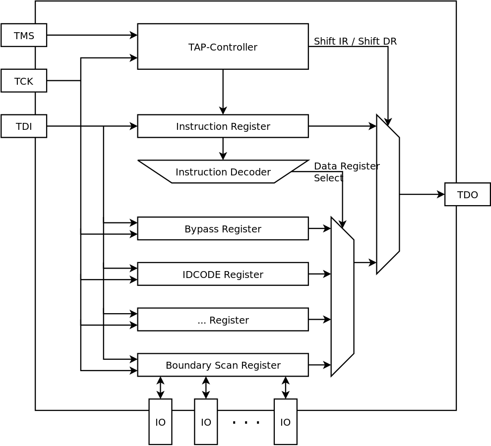
Basic understanding of how JTAG works will be helpful when using JTAGenum.
There are 4 lines/pins:
TDO=output, TDI=input, TCK=clock, TMS=state machine control.
Say you want to read the ID of the chip.
First you would send the IDCODE instruction to the instruction register (IR).
The JTAG controller then places the actual id code value of the chip in a data register which you could then read out.
You would think that it would be enough to have one input line going to the IR and one output coming from the DR
but JTAG also supports writing to the DR.
As apposed to adding another input line specific to the DR instead JTAG works by moving the input and output lines between IR and DR.
The TMS line is used to switch TDI/TDO to IR when you want to place an instruction and back to DR
when you want to read or write data.
With all operations, be it state change (TMS) reading (TDI) or writing (TDO),
the clock line must be cycled once (TCK) for every bit or change.
This was a brutal and drastic simplification but with that understood reading the Usage section should be comprehensible.
This document can also be found at:
 http://deadhacker.com/2010/02/03/jtag-enumeration/
authors and code branches:
 cyphunk  http://github.com/cyphunk/JTAGenum/
 jal2     http://github.com/jal2/JTAGenum/
 zoobab   http://new.hackerspace.be/JTAG_pinout_detector
 z1Y2x    https://github.com/z1Y2x/JTAGenum/

For questions, help, changes, repository write access or
interesting targets: cyphunk@gmail.com with gpg 0x490F3380

 浙公网安备 33010602011771号