
LPC43xx SGPIO Experimentation
LPC4350 SGPIO Experimentation
The NXP LPC43xx microcontrollers have an interesting, programmable serial peripheral called the SGPIO (Serial GPIO).
It consists of a slew of counters and shift registers that can be configured to serialize and deserialize many channels of data.
Channels can be grouped to create multi-bit parallel data streams.
AN11210 Using SGPIO to emulate an SPI master interface
AN11275 SGPIO on the LPC4300 - Emulating PWM via SGPIO
AN11343 SGPIO camera module design using LPC4300
AN11351 Implementing a UART using SGPIO on LPC4300
AN11196: Camera interface design using SGPIO
SGPIO_I2C_Implementation
• 每个SGPIO 输入/ 输出位串都可用于执行串行到并行或并行到串行数据转换。
• 16个SGPIO输入/输出位串(每个都带32位FIFO)可利用移位时钟的每个周期将来自引脚的输入值或对引脚的输出值移位。
• 每个位串都支持双缓冲。
• FIFO 已满、转换时钟或模式匹配时生成中断。
• 可将位串级联以增加缓冲区大小。
• 每个位串有一个32 位模式匹配滤波器。
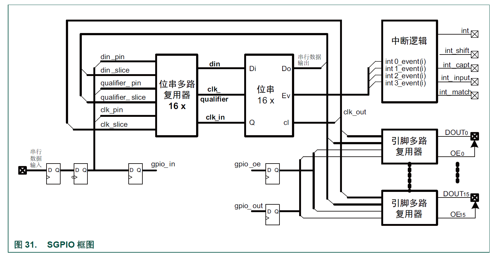
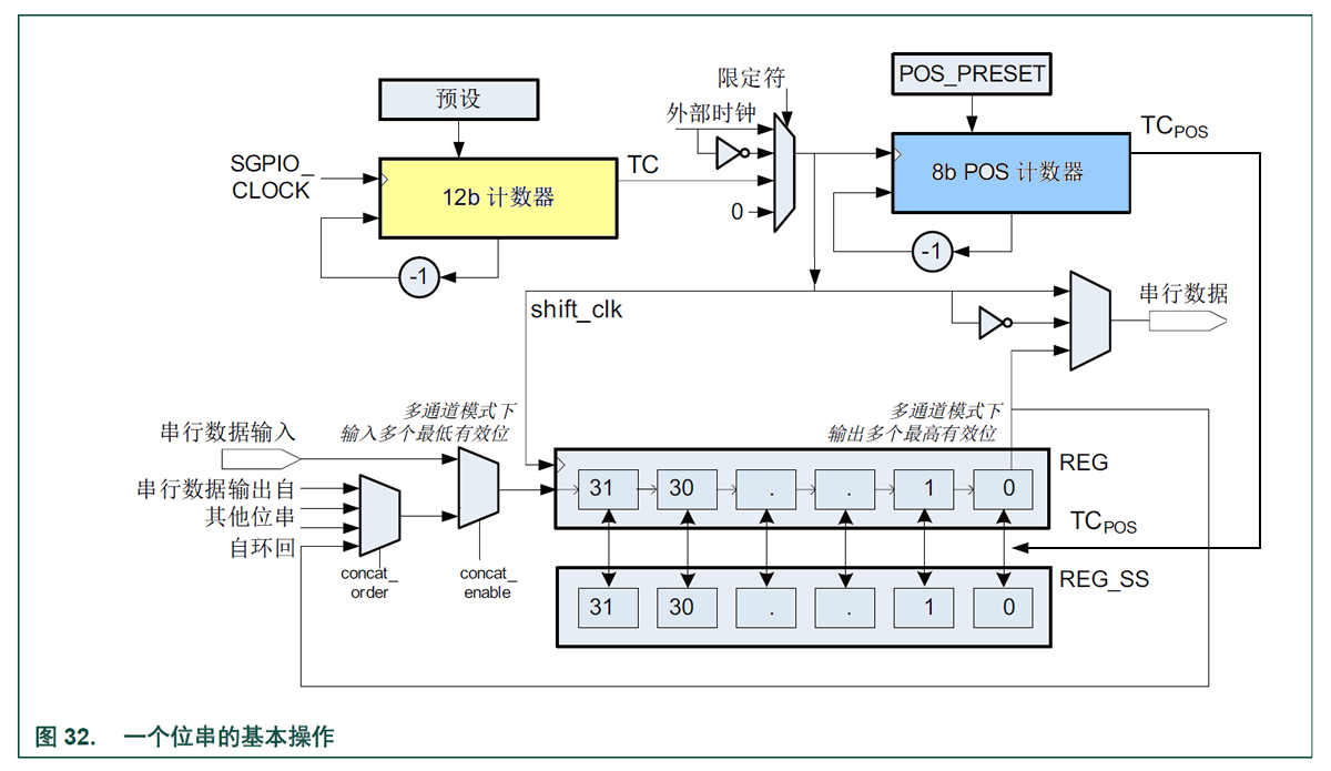
串行GPIO (SGPIO) 提供标准GPIO 功能,并具备加速串行数据流处理的增强功能。
单一SGPIO 输入/ 输出或双路、四路和字节通道数据输入/ 输出上的数据流使用所谓的位串进行处理。
最多可支持16个位串,所有16个位串的基本功能集相同,某些位串还具有其他功能。
• 位串:
– 每个位串支持32 位FIFO,在每个移位时钟从某个引脚移入或移出至某个引脚。
– 某些位串控制引脚输出使能。
– 位串为双缓冲; POS 计数器达到0x0 时,位串与影子寄存器进行交换。
– 可将位串级联以增加缓冲区大小。如果位串n与位串m级联,则软件应当确保POS[n]和POS[m] 相等且同相运行。
– POS 计数器达到0x0 时产生中断。
– 支持并行到多数据流串行转换,反之亦然。转换支持交错并联;每次最多转换8 位(n= 1、2、4 或8 分别对应串行、双串行、四串行和字节并行IO)。
• 时钟:
– 以SGPIO_CLOCK 运行的12 位计数器创建移位时钟来捕获输入或创建输出值。
请注意,输入频率应当小于SGPIO_CLOCK 频率的一半。
– 外部输入可用作移位时钟。有效边沿可以为上升沿或下降沿(但不能同时为两者)。
– 外部输入可用作移位时钟门控。有效电平可以是低电平或高电平。
– 内部信号可用作移位时钟门控。
– 以移位时钟运行的POS 计数器使能双缓冲。
• 输入:
– 使用移位时钟捕获输入。
– 输入可在输入电平(低电平或高电平)或跳变(上升、下降上升或下降)时产生中断。中断可被掩码。
– 可在模式匹配时产生中断。模式最多为32 位长并且可被掩码(匹配值= “不关注”)。4 个位串(A、I、H 和P)支持掩码功能。
– 4 个输入可用作其他位串的移位时钟来捕获其他输入。
• 输出:
– 创建输出:有效电平(低电平或高电平)或三态。注意,如果位串用于创建速率为fout 的输出时钟,则位串时钟的速率至少应为2x fout。
这样每个位串的数据速率就被限制为SGPIO_CLOCK 速率的一半。
– 输出使能可由其他位串控制。如果是多通道输出,则可独立于MSB 线控制LSB 通道输出使能。
– 从移位时钟计数器创建输出时钟。
– 输出时钟极性可反转。
• 接口:
– 寄存器存储器映射支持ARM “存储多个”和“加载多个”指令的使用。控制相同特性的位串功能在地址连续的寄存器中映射。
– 位顺序针对MSB 优先进行优化。需要LSB 优先的接口应当使用软件指令(RBIT) 来反转位顺序。
中断
• 下列事件中将产生中断:
– COUNTx 等于零、出现移位时钟时提出移位时钟中断(参见表222 至表227)。该中断在每个移位位生成。
– 发生位串交换时(即POSx 等于零、出现捕获时钟时),提出捕获时钟中断(参见表228 至表233)。
– 输入数据等于掩码的模式时提出模式匹配中断(参见表234 至表239)。
– 输入位与DATA_CAPTURE_MODE 中设置的条件相等时提出输入位匹配中断(表240 至表244)。
• 每个中断可由一组寄存器采用以下某种方法进行控制:
– 通过寄存器CLR_EN/SET_EN 禁用或使能中断。
– 通过寄存器STATUS 读取中断。
– 通过寄存器ENABLE 读取中断掩码。
– 通过寄存器SET_STAT 设置中断。
– 通过寄存器CTR_STAT 清除中断。
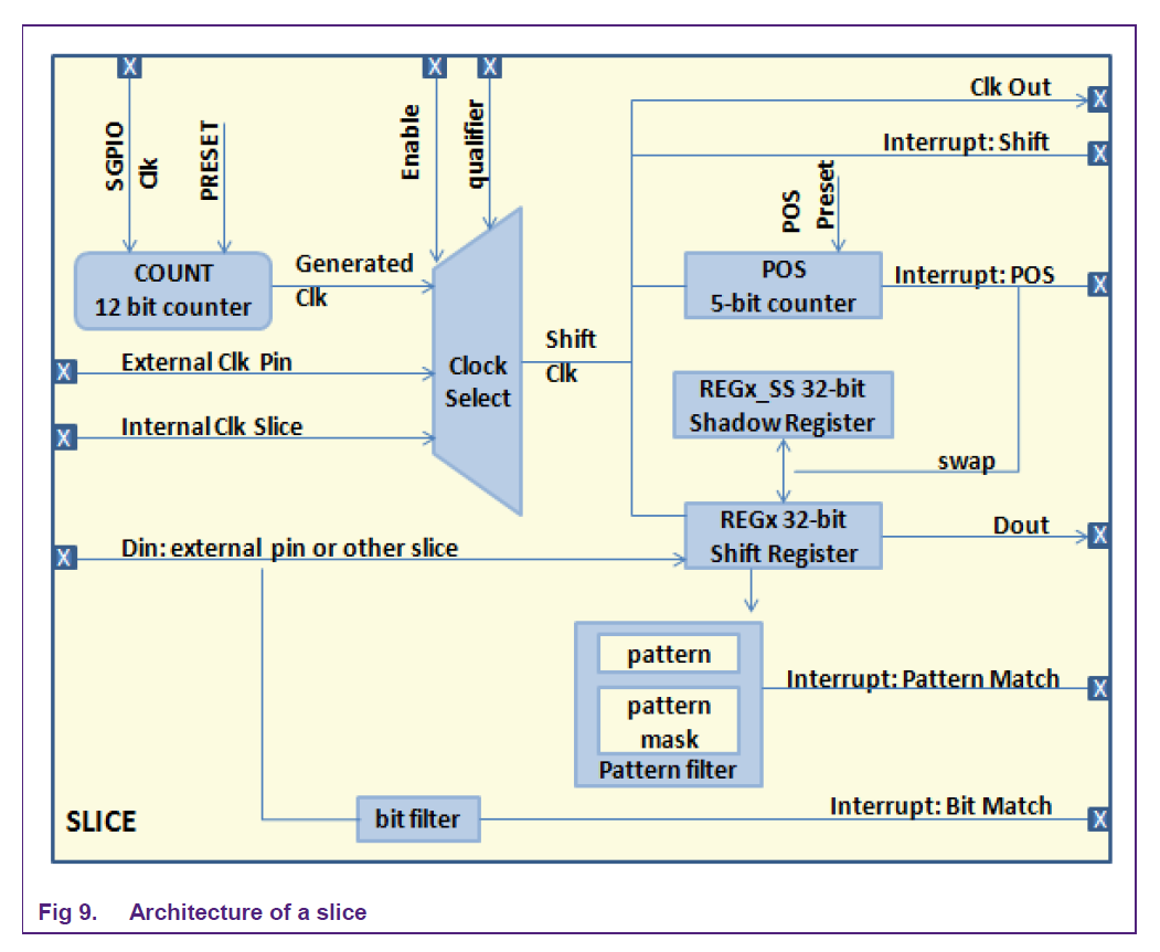
串行GPIO (SGPIO) 提供标准GPIO 功能,并具备加速串行数据流处理的增强功能。
增强型功能使用所谓的位串构成。
所有16 个位串具有相同的基本功能集。
某些位串还具有附加功能,可用于模式匹配和处理2 位、4 位或8 位宽的数据流。
位串执行并行到串行数据转换(反之亦然)。
一个位串包含32 个以链条形式连接在一起的1 位寄存器(REG)。
数据通过链条右移。输入数据在MSB 处移入,从LSB 移出。
输入数据被同步;这就产生了一个SGPIO_CLOCK 周期的延迟。
更改引脚方向时,尤其是在模拟高速双向总线时,应考虑该延迟。
移位时钟控制数据通过链条移位的速率。
位的移位增量由寄存器parallel_mode 设置为1位、2 位、4 位或8 位。
多通道模式中使用大于1 的移位。
移位时钟可来自外部源(参见<tbd>)或从本地生成。
移位时钟可由外部引脚或其他位串来限定。
本地时钟由以SGPIO_CLOCK 运行的12 位下行计数器COUNT 构成。
计数持续时间可通过寄存器PRESET 预设。
COUNT 达到零时用PRESET 加载。
移位时钟频率因此与频率(shift_clock) = 频率(SGPIO_CLK) / (PRESET+1) 相等。
每当COUNT 达到零时寄存器右移;
用捕获自DIN 的数据加载位REG[31],用位REG[0]加载DOUT。
因此,COUNT 控制串行数据速率。
当几个位串用于创建接口端口时,不同位串间的相位可通过使用不同的CONUT 初始值来控制。
另外一个下行计数器(POS) 控制并行数据加载到链条和从链条存储的时间。
POS 计数器由COUNT 等于零时会递减的8 位计数器组成。
POS 达到零时,用PRESET_POS 值加载。
位串数据使用双缓冲方案进行交换。
POS 达到零时,位串寄存器REG 的内容与位串缓冲区REG_SS 的内容交换。
这使得CPU 有更多时间来处理REG_SS 缓冲区的内容。
PRESET_POS 可用于指示并非32 位的倍数的字的字边界。
如果PRESET_POS 值为零,则在每个移位时钟后REG 会与REG_SS 交换。
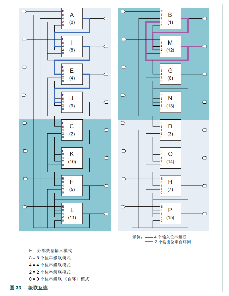
级联
可将位串级联以增加缓冲区大小,使其超出REG_SS。借助该功能,还可通过执行反向级联来创建PWM 流。
级联由寄存器SGPIO_MUX_CFG 设置。通过字段CONCAT_ENABLE 使能该功能。
多个位串级联时,该字段的设置对所有相关位串应相同。
字段CONCAT_ORDER 设置级联的大小。
对于大小为零的自环模式,位串输出会传回到位串输入。该模式可用于创建重复数据流。
图33 显示了哪些位串可级联。
位串排列在4 个组中,以位串A、B、C、D 开始。
每个组由4 个级联位串组成。
例如,位串A 输入可使用3 个额外位串I、E 和J 来扩展。
如果是输出模式,则位串I 可由位串A、I 和E 扩展。
位串进一步排列在四个子组中,以E、F、G、H 开始。
这些子组支持两个位串的级联。位串A 和B 最多支持7 个位串的级联。
如果多个位串级联,则这些位串的concat_order 应当一致。
就上例而言,输入位串A 应设置为输入(concat_enable=0)。
如果未设置concat_enable,则concat_order 值为“不关注”值。
对于位串I、E 和J,设置concat_enable=1 并使用concat_order =10(4 个位串)。
级联位串应当具有一致的移位时钟和位移位设置(SLICE_MUX_CFG 中)。
K 个位串级联时, PRESET_POS 应设置为0x20 x K - 1。
模式匹配
所有位串均具有模式匹配功能。
该功能可用于检测启动代码等。要使用该功能,则必须用需匹配的模式来对REG_SS 编程
(请注意, POS 达到零时REG_SS 不会与REG 交换!)
MATCH_MODE 位必须设为1。输入数据现在与已编程的模式相比较。发现匹配时会提出模式匹配中断。
四个位串(A、H、I 和P)同样支持对模式的掩码;必须设置MASK_x 以便对模式位进行比较(‘1’表示比较)。
例如,寻找模式0x1234.xxxx.5678.9ABC 时,
REG 应设置为0x1234.xxxx.5678.9ABC,
MASK 设置为0xFFFF.0000.FFFF.FFFF。
引脚复用
位串输入和输出通过本地引脚多路复用器连接到全局引脚多路复用器(第15 章)。
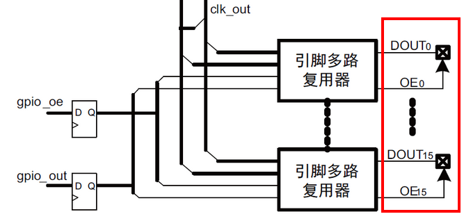

多路复用数字引脚将分组到16 个引脚组,即P0 到P9 和PA 到PF,每组最多使用20 个引脚。
每个数字引脚可以支持多达8 种不同的数字功能,包括通用I/O (GPIO),可通过SCU寄存器进行选择。
此外,某些引脚支持通过ENAIO 寄存器可选的模拟功能(ADC 输入和DAC 输出)。
请注意,引脚名称并不表示所指派的GPIO 端口。
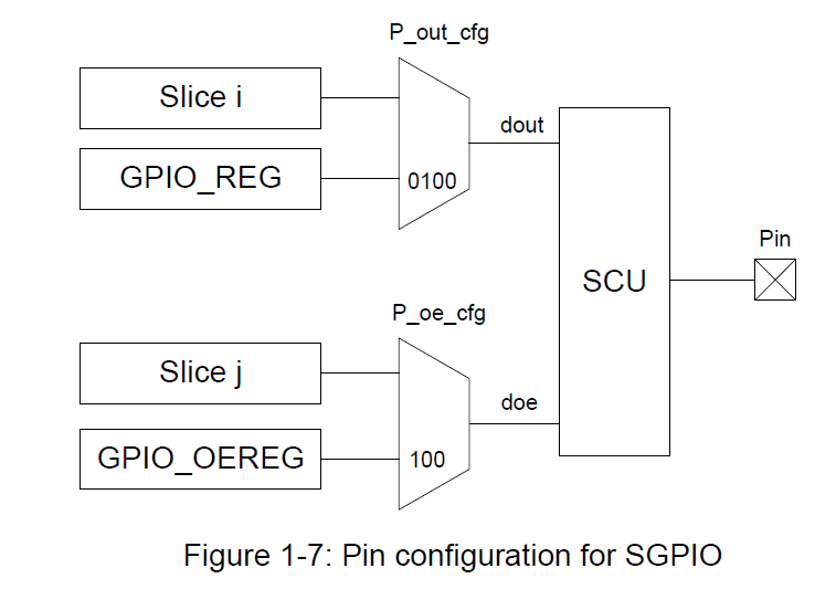
针对普通GPIO功能(输入、输出、输出使能),每个引脚同样可
使用寄存器GPIO_INREG、GPIO_OUTREG 和GPIO_OEREG 来控制。
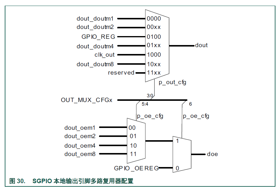
引脚多路复用器配置寄存器(OUT_MUX_CFG0 至15)
每个寄存器控制一个本地输入引脚多路复用器:OUT_MUX_CFG0 至OUT_MUX_CTRL15控制引脚SGPIO0 至SGPIO15。
注:引脚指的是LPC43xx 上的引脚,通过引脚配置寄存器配置为SGPIOn 引脚。
P_OUT_CFG 位控制位串生成数据时数据流的宽度或输出是用作GPIO 还是时钟。并非所有模式都受所有位串的支持。
表203 显示了SGPIOn 引脚如何连接至位串。例如, 8 位宽模式仅受位串A/B、J/M 或L/N 支持。
使用位宽大于1 的模式时,每个时钟的移位位数应设置为与并行模式的宽度相等(参见表207 中的位PARALLEL_MODE)。
P_OE_CFG 位控制输出使能源。可使用寄存器GPIO_OEREG 以静态方式或由其他位串以动态方式来进行控制。
表204 指示哪些位串控制哪些引脚的输出使能。
请注意,对于位宽大于1 的模式,输出使能由2 位定义:
一位用于LSB,一位用于余下的全部MSB。
使用位宽大于1 的模式(P_OE_CFG = dout_oem2、dout_oem4 或dout_oem8)时,每个时钟的移位位数应设置为每个时钟2 位。
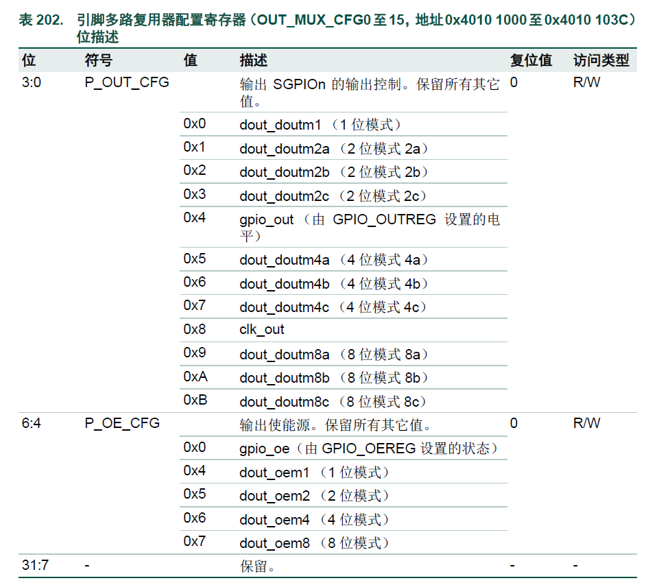
表203 显示了输出多路复用方案。这些设置由寄存器OUT_MUX_CFG 控制。
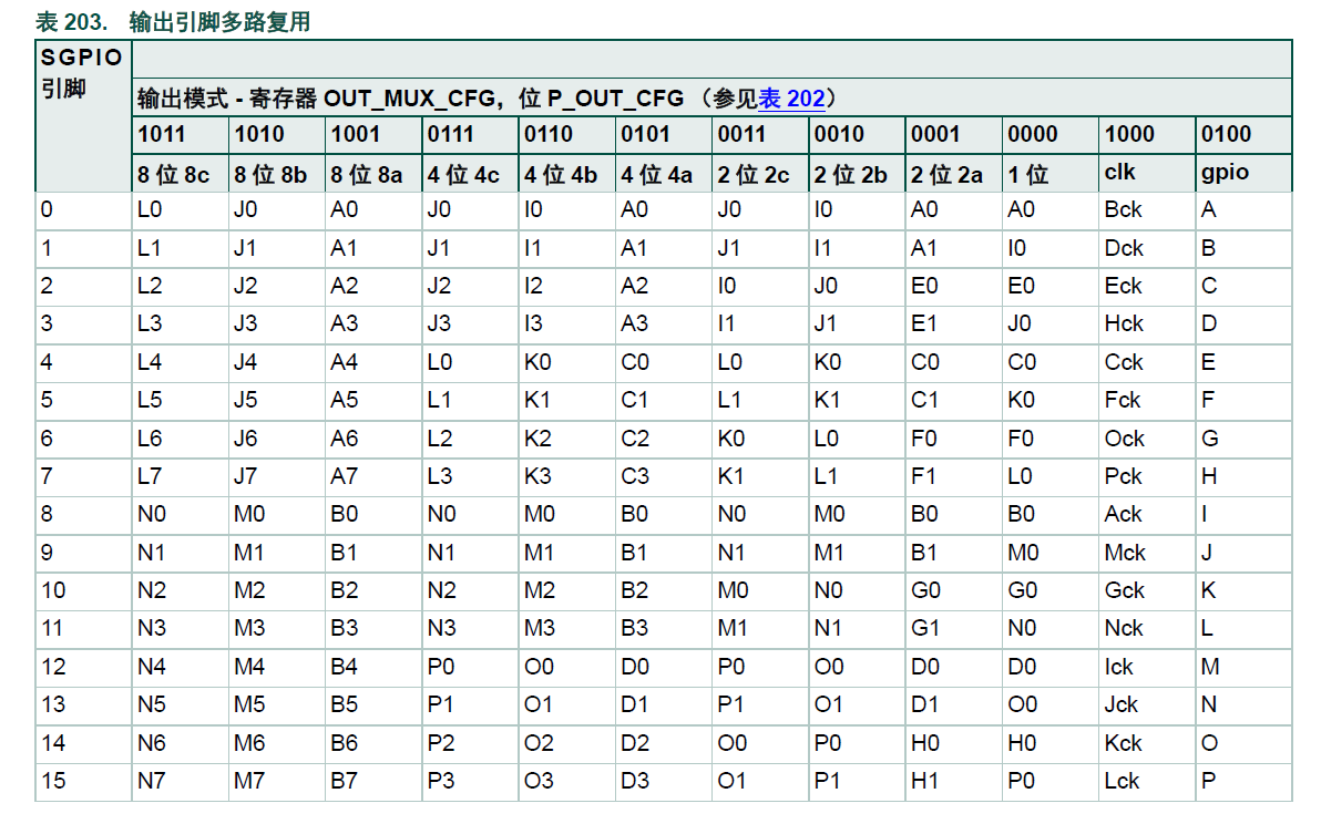
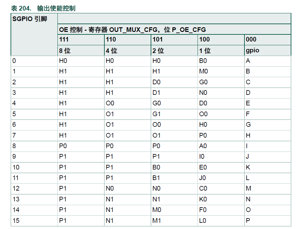
表244 显示了输入多路复用方案。
这些设置由寄存器SGPIO_MUX_CFG 控制。
每个寄存器控制一个SGPIO 多路复用器来选择下列源:
• 外部时钟源(未使用COUNT 时)
• 外部时钟门控(静态或由位串或外部引脚控制)
• 输入级联结构
SGPIO_MUX_CFG0 至SGPIO_MUX_CFG15 控制位串A(寄存器0)至P(寄存器15)。
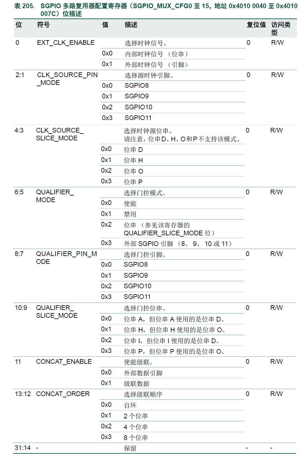

要避免振荡,可作为其他位串的时钟源的位串本身不能支持外部位串时钟(CLK_SOURCE_SLICE_MODE)。
这些位串不应将高于SGPIO_CLOCK/2 的时钟输入到其他位串。
16 个位串以A 到P 表示。后缀表示与引脚连接的位串位,
例如, 8 位并行输入模式下,引脚SGPIO0 至7 连接到位串A 位31 至24。
并非所有功能都可用于所有引脚。
例如,仅引脚SGPIO9 至11 可用作时钟源输入或门控输入或门控输出。
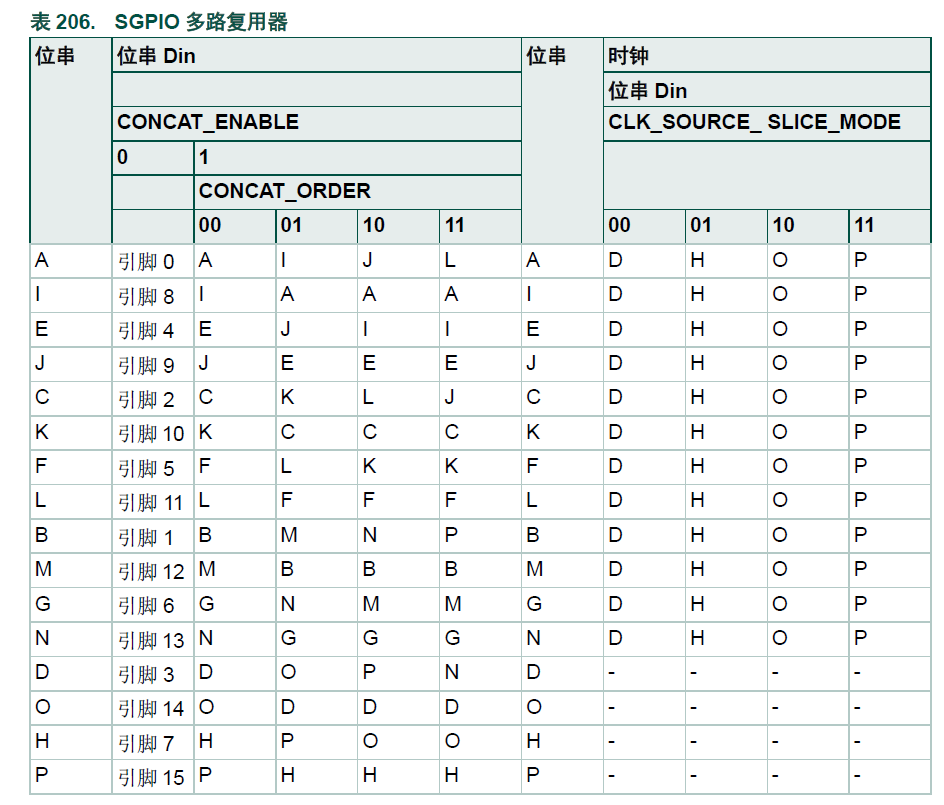
时钟源可以来自引脚8、9、10 或11,也可以来自位串D、H、O 或P。
请注意,可用作时钟源的位串不能以自身或其他位串作为时钟源。
外部时钟与内部SGPIO 时钟同步。为防止混叠,时钟源频率应小于SGPIO 频率的一半。
门控信号来自引脚8、9、10、11 或位串A、H、I、P。
由于位串无法将门控反馈给自身,因此还使用其他一些位串。
位串D 可作为位串A 和位串I 的门控,位串O 可作为位串H 和位串P 的门控。
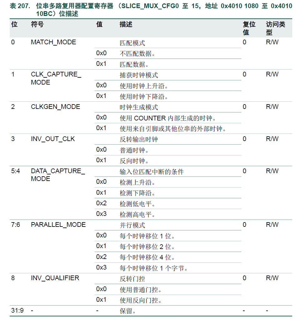
位串多路复用器
位串多路复用器选择外部位串时钟和位串时钟门控。
位串多路复用器配置寄存器(SLICE_MUX_CFG0 至15)
每个寄存器控制一个位串多路复用器移位时钟以及每个时钟移位位串FIFO 的多少位。
寄存器SLICE_MUX_CFG0 至SLICE_MUX_CFG15 控制位串A (寄存器0)至P (寄存器15)。
位MATCH_MODE 选择匹配滤波器是否有源或是否捕获了数据。
仅位串A、H、I 和P 支持使用掩码的匹配(寄存器MASK_x)。对于其他位串,不对模式进行掩码。
位CLKGEN_MODE 选择由位串计数器、外部引脚或其他位串生成的时钟作为移位时钟。
位INV_OUT_CLK 可反转移位时钟。这应当仅用于来自引脚的外部时钟。
Data_capture_mode 用于定义哪种输入数据条件可生成中断。
有关将位串数据连接到引脚以便对位PARALLEL_MODE 进行多种设置,请参见表207。

内部连接
SGPIO 引脚10 和12 可启动12 位ADC。
SGPIO 引脚14 和15 可启动GPDMA 复位。
SGPIO 引脚3 和12 连接至SCT 和定时器捕获输入。对于I2S 应用,SGPIO3 和SGPIO12
引脚同样支持128 分频的信号(SGPIO3_DIV 和SGPIO12_DIV)。
启动信号可由相关的位串创建(例如,引脚15 由1 位输出模式下的位串P 控制),或使用
GPIO 模式下的这些引脚创建。
AN11275 SGPIO on the LPC4300
What is SGPIO
Serial GPIO is a new digital configurable peripheral available on the LPC43XX devices from NXP.
With SGPIO it is possible to create serial data protocols with very little CPU load compared to bit banging.
SGPIO's basic building block is slice.
The slice is the hardware part that handles the data processing when sending or receiving data.
There are a total of 16 SGPIO slices and 16 SGPIO IO pins in the SGPIO interface.
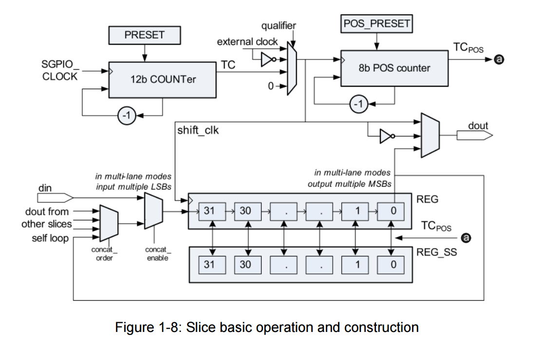
Fig 1 shows the basic components inside a slice.
A slice basically consists of a 32-bit FIFO (main register REG in Fig 1) that is used to clock data in or out,
a shadow register (REG_SS register in Fig 1) for setting up the output data or receiving the input data,
a 12-bit down counter to generate the shift clock and an 8-bit down counter to control the number of bits shifted in or out.
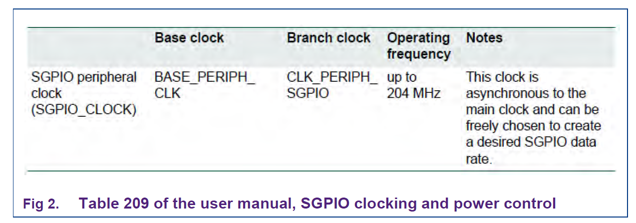
The slice’s shift clock can be sourced from the SGPIO peripheral clock (SGPIO_CLOCK).
Please refer to Fig 2 below to understand SGPIO_CLOCK’s base clock, and section 5.1 for more SGPIO_CLOCK setup.
At every SGPIO_CLOCK, the 12-bit down counter (COUNT in Fig 1) counts down by 1.
When this 12-bit down counter (COUNT) reaches zero, a data bit is shifted in or out of the FIFO (main register REG).
Then COUNT is reloaded with the value in the PRESET register.
Therefore, the value in the PRESET register determines the shift clock speed.
Frequency (shift clock) = Frequency (SGPIO_CLOCK) / (PRESET+1)
Each slice includes an 8-bit down counter (register POS in Fig 1) that controls the number of bits shifted in or out of the slice.
Every time the COUNT register reaches zero a data bit is shifted in or out of the FIFO and the POS register decrements by 1.
When the POS register reaches zero it is reloaded with the value in POS_PRESET
and the main register REG and its shadow register (REG_SS)’s contents get exchanged.
For an output slice new data is written to the shadow register and when the slice is done sending the data in the main buffer the two buffers get exchanged.
For an input slice new data is clocked in the main buffer and when the slice is done collecting the data in the main buffer the two buffers get exchanged.
Hence, to exchange the main register and the shadow register every m bit the POS_PRESET should be set up as m-1.
To exchange the content every k*32 bit POS_PRESET should be 0x20 * k – 1.
This setting should be used when k slices are concatenated.
Tip 1:
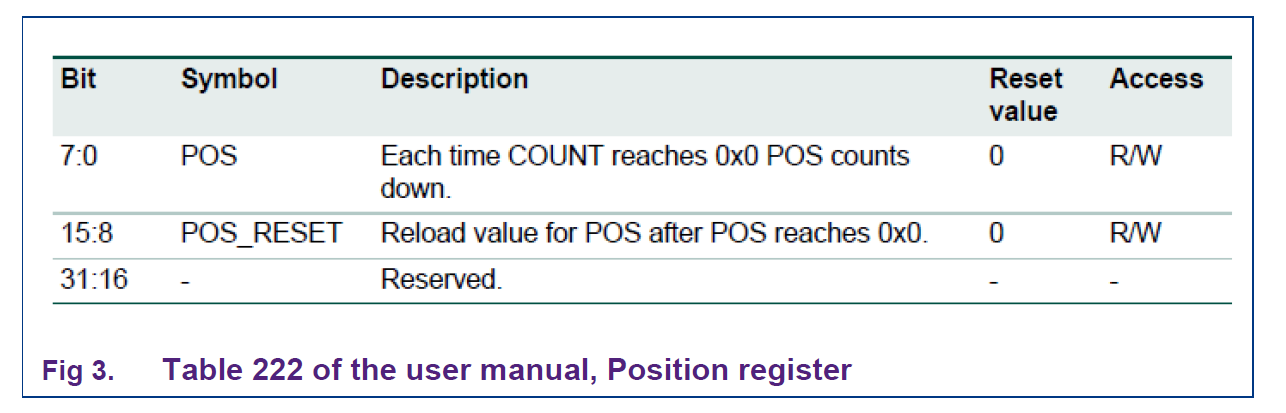
The POS register is divided into two parts, the POS counter and the POS counter’s preset value.
Please refer to Table 222 in the user manual for details.
Tip 2:
An SGPIO pin is not the same as an SGPIO slice;
a pin number is not equal to a slice number!
A slice connects to an SGPIO pin using a pin mux.
Because of this one slice can be connected to multiple pins
and multiple slices can be concatenated to one SGPIO pin.
An SGPIO slice can be connected to 1, 2, 4 or 8 SGPIO pins.
Up to eight slices can be concatenated to input or output through one SGPIO pin.
Tip 3:
The slices are identified by letter A to letter P.
Slice A is the first slice, slice B is the second slice and so on.
SGPIO usage
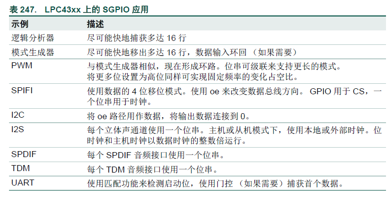
SGPIO can be used to "emulate" serial protocols in those cases when an additional SPI/I2C/UART is needed.
SGPIO can also be used to create fast serial and parallel protocols like PWM,
e.g., reading in parallel data from a camera module and display/VGA generation.
The max speed of a clock signal that can be generated with SGPIO is half the clock speed of the CPU.
Therefore, the absolute max speed of the SGPIO_CLOCK is 102 MHz when using the maximum 204 MHz CPU clock.
A complex example for a 7.1 soundcard can be downloaded from
http://lpcware.com/content/project/lpc4350-hitex-board-getting-started-guide
It connects to a computer via USB and uses SGPIO to send audio data from USB to four stereo I2S DACs.
Register descriptions
SGPIO is an extremely flexible peripheral.
With that flexibility a lot of options are possible, but it also means there are a lot of registers to set up.
The registers are divided in four groups:
- 1. Registers for slice/SGPIO pin multiplexing control
- 2. Registers for slice operation control (double buffering and shift clock control)
- 3. Registers for interrupt specific settings
- 4. Registers for SGPIO pin control
Note:
The following information is meant to accompany and expand on chapter 18.6 of the user manual,
which provides an explanation of all available register settings in the SGPIO.
4.1 Slice/SGPIO pin multiplexing registers
For this group of registers, replace ‘x’ with the correct number for the slice.
0 for slice A, 1 for slice B, 2 for slice C and so on.
4.1.1 OUT_MUX_CFGx
The OUT_MUX_CFG register is used to set up the output mode of the slice and how many I/O pins are used in an output slice.
It is possible for one SGPIO slice to use 1, 2, 4 or 8 I/O pins.
Bits 3:0 control how many pins are used in the different slice output configurations
or whether the corresponding pin is for shift clock output or GPIO output.
1-bit mode, 2-bit mode, 4-bit mode, 8-bit mode, clk_out, gpio_out
Bits 6:4 determine how the output enable is controlled.
The output enable can be controlled by the GPIO_OENREG register
or by a different slice according to the configuration above.
The output states include low or high in active mode or tri-state when disabled.
In the following table the output pin multiplexing can be found.
For example, when SGPIO pin 1 is used in 1-bit mode the corresponding slice is slice I.
4.1.2 SGPIO_MUX_CFGx
With the SGPIO_MUX_CFG register the clock and concatenate settings can be changed.
Bit 11 is used to enable slice concatenation. contact_enable
When contact_enable is high the SGPIO slice will send the data in the main register, exchange the data and shadow register,
and send the data in the main register again.
If contact_enable bit is low it will stop after the first exchange. [ data from din_pin ]
To use an external pin as shift clock : bit 0 should be 1
and the clock pin can be selected with bits 2:1 : SGPIO pin 8, 9 10 and 11 can be used as an external clock input.
With bits 13:12 it is possible to concatenate multiple slices to create a bigger FIFO buffer according to the following table.
For example, if slice A is chosen as an input slice and a 4 slice big FIFO buffer is used the buffer will look like this:
- 1. After the FIFO from A is shifted, the FIFO of slice I follows.
- 2. After slice I the FIFO of slice E follows.
- 3. After slice E the FIFO of slice J follows.
- 4. After slice J is complete, the main registers of slice A, I, E, J are exchanged with their own shadow registers.
- 5. The input then starts from slice A again, followed by slice I, E, J.
NOTE: In the programming code the data registers of slice A, I, E and J should all be handled and should be seen as one big 128-bit FIFO buffer.
4.1.3 SLICE_MUX_CFGx
With the SLICE_MUX_CFG register, a couple of settings can be used.
When using the data match interrupt bit 0 has to be high.
When using data match mode, the slice’s shadow register should hold the pattern to be matched.
In addition, when data match is enabled the main register and the shadow register will not exchange when FIFO is done with input or output data.
With bit 2 the clock input can be chosen;
0 for the internal clock and 1 to use an external clock.
It works only when this bit and SGPIO_MUX_CFG are set to use an external clock.
With bits 5:4 the input bit match interrupt mode can be selected: 0b00 for rising edge,
0b01 for falling edge, 0b10 for low level, 0b11 for high level.
With bits 6:7 the amount of bits that are shifted out per clock can be chosen.
When a slice has multiple I/O pins this value has to be set accordingly:
0b00 for 1 bit, 0b01 for 2 bits, 0b10 for 4 bits or 0b11 for 8 bits per clock.
4.2 Slice operation control registers
4.2.1 REGx
This is the data register.
As long as a slice is enabled it will shift a data bit in or out at every shift clock.
Data is right shifted, data is shifted in at bit 31 and data is shifted out from bit 0.
4.2.2 REG_SSx
This is the shadow register for the data.
Every time a slice is done with sending or receiving data it exchanges the data and shadow register.
This way the shadow register can be read or written at any time.
4.2.3 PRESETx
With the PRESETx register the SGPIO_CLOCK can be divided down to a lower speed.
To calculate the value for this register the following formula is used:
PRESETx value = (SGPIO_CLOCK speed / shift clock speed) – 1.
When a 1.5 MHz clock speed is required for a slice and a 12 MHz SGPIO clock is used the correct PRESETx value is (12/1.5) – 1 = 7.
4.2.4 POSx
Each position register contains the position counter for one slice:
POS0 to POS15 contain the counter for slice A (register 0) to slice P (register 15).
This register controls when the shadow register REG_SS content is exchanged with main register REG.
It has [15:8] as the POS_PRESET value and [7:0] as the current data bit POS counter.
At each data bit shift, POS decrements by 1.
When POS reaches zero, POS is restored with its POS_PRESET value.
This should be 31 when the main register and the shadow register exchange after all 32 bits of data have shifted in or out.
But when concatenating k slices this value should be (0x20 * k -1).
For example, when concatenating 4 slices and every slice needs to shift in or out all of its 32-bit data, POSx should be (32 * 4 - 1) = 127.
Please refer to Fig 3 for some more details for this register.
Tip 4.
Before a slice is started (using CTRL_ENABLE), POS should be set to the POS_PRESET value.
4.2.5 MASK_A, MASK_H, MASK_I, MASK_P
The mask registers are used for the “on pattern match” interrupts.
With some slices it is possible to mask the data for the pattern match interrupts.
Slices A, H, I and P support this function.
Every bit that is 1 in this register will be masked.
If this register contains the value 0b00001111 the first 4 bits will be masked for the pattern interrupt.
See chapter 6, SGPIO Interrupts for more information.
4.2.6 CTRL_ENABLE
With the CTRL_ENABLE register set to 1 for a particular bit the corresponding slice’s 12-bit COUNT down counter
or external shift clock is started to provide the data shift clock for the slice.
4.2.7 CTRL_DISABLE
With the CTRL_DISABLE register set to 1 for a particular bit the corresponding slice’s COUNT clocks
or external shift clock is disabled.
When this register is set, it synchronously disables the POSx counter when POSx counter reaches a zero count.
The CTRL_DISABLED register is not cleared at that time: it remains set.
Tip 5.
When starting COUNTx (by setting CTRL_ENABLE), this register should be set after COUNTx is started with register CTRL_ENABLE.
4.3 SGPIO interrupt specific registers
For these interrupt specific registers, replace the x with the correct number for the interrupt.
0 for shift clock; 1 for main register and shadow register exchange;
2 for data pattern match and 3 for input bit match.
4.3.1 CLR_EN_x
This register is used to disable interrupts. Slice interrupts can be disabled by writing a 1 to the register.
For example, if a 1 is written to bit 2 the interrupt for slice C will be disabled.
4.3.2 SET_EN_x
This register is used to enable interrupts. Slice interrupts can be enabled by writing a 1 to the register.
If, for example, a 1 is written to bit 3 the interrupt for slice D will be enabled.
4.3.3 ENABLE_x
Reading out this register will return what slices have their interrupts enabled.
If this register contains the value 0b1001 that means slice A and D have the interrupts enabled.
4.3.4 STATUS_x
Reading out this register will return on which slices an interrupt has happened.
It is possible that an interrupt happens on multiple slices at the same time.
If this register contains the value 0b1000100 interrupts happened on slice C and G.
4.3.5 CTR_STAT_x
This register is used to clear the interrupt state.
It is recommended to clear all interrupt states after handling the interrupts otherwise the value in the STATUS_x register will also contain old interrupt states.
4.3.6 SET_STAT_x
This register is used to set interrupt states. When a 1 is written to bit 0 it will look like an interrupt happened on slice A. This register can be used for code testing.
4.4 SGPIO pin control registers
These registers are used to control SGPIO pin status.
GPIO_INREG, GPIO_OUTREG and GPIO_OENREG are SGPIO pin based.
This means that they control SGPIO pins and not slices.
If a 1 is written to bit 2 this will effect SGPIO pin 2 and not slice C.
4.4.1 GPIO_INREG
With this register the SGPIO pins can be made an input. When a 1 is written to bit 2 SGPIO pin 2 will be an input.
Note: The SGPIO pin must be made an input with the pinmux too.
See chapter 15 of the user manual from the LPC4300 for more information about the pinmux.
NOTE: Concatenate cannot be set to self loop when using an SGPIO pin as input.
4.4.2 GPIO_OUTREG
With this register the SGPIO pins can be made an output. When a 1 is written to bit 3 SGPIO pin 3 will be an output.
4.4.3 GPIO_OENREG
With the GPIO_OENREG register an SGPIO output pin can be enabled.
An SGPIO pin must be enabled in order to work.
When a 1 is written to bit 3 SGPIO pin 3 will be enabled.
To disable an SGPIO pin a 0 has to be written to the corresponding bit.
5. Steps to get SGPIO working
To get SGPIO up and running:
- 1. Select the right clock
- 2. Set up the registers, slices used, IO pins used, concatenate slices, etc.
- 3. Set up the interrupts
- 4. Handle interrupts and data
5.1 Selecting the right clock signal
First the clock speed has to be selected.
By default SGPIO uses the IRC, which runs at 12 MHz. Other clock sources can be selected too;
by selecting PLL1 SGPIO can run on the same clock speed as the LPC4300.
In the PWM example the following line of code can be found in lpc43xx_cgu.c:
IRC:
LPC_CGU->BASE_PERIPH_CLK = (0x1 << 24);
PLL1:
LPC_CGU->BASE_PERIPH_CLK = (0x9 << 24);
For more information, see page 105 of the LPC4300 user manual.
5.2 Set up the registers
After knowing how many SGPIO pins are going to be used, and how they will be used, the registers can be set up.
The registers that need to be set up are
OUT_MUX_CFGx, SGPIO_MUX_CFGx, SLICE_MUX_CFGx,
PRESETx, COUNTx, POSx, REGx and REG_SSx.
The first three registers control most of the slice settings such as:
number of slices concatenated, number of SGPIO pins per slice, input or output, what clock is used etc.
Depending on the interrupts used to handle the data the interrupt registers must be set up too.
Also in the pinmux the IO pins must be set up as SGPIO pin and as input or output.
To start SGPIO the clock signals must be enabled.
This is done by setting bits 15 and 12 in the CTRL_ENABLED register.
An example how to set up the SGPIO registers for I2S use can be found in the user manual on page 376 to 379.
5.3 Set up interrupts
The interrupt description can be found in chapter 6 of this document.
5.4 Handling data
When everything is set up and SGPIO is running the data still needs to be handled.
What to do with the incoming and outgoing data is up to the user and depends on the application.
When emulating a bus protocol like UART, SPI or I2C the protocol itself has to be made by software.
Data arrives in 32-bit blocks.
UART uses 10-bit blocks (start bit, 8-bit data, stop bit) and SPI and I2C use 8-bit blocks.
This translation has to be made in software and is different per bus protocol.
When using SGPIO to communicate with a camera module or some other parallel bus the same story applies.
Speeds over 40 MHz are doable and CPU load can be lowered by concatenating slices.
When using 4 or 8-bit wide busses it is recommended to concatenate 2, 4 or 8 slices for a larger buffer.
If the buffer is 32-bit and an 8-bit bus is used the buffer is full in just 4 SGPIO clock cycles.
When 8 slices are concatenated a 256-bit buffer is created and it takes 32 SGPIO clock cycles to fill this buffer, a much lower CPU load.
6. SGPIO Interrupts
There are four interrupt methods available for SGPIO, they are:
- 1. On shift clock
- 2. On data exchange clock
- 3. On data pattern match
- 4. On input bit match (rising/falling edge, high/low level)
6.1 On shift clock
When enabled through SET_EN, this interrupt occurs every time COUNTx equals 0.
This normally happens every time 1 data bit is clocked out or in of an SGPIO slice and can be CPU intensive.
The registers used for this interrupt are:
• CLR_EN_0
• SET_EN_0
• ENABLE_0
• STATUS_0
• CTR_STATUS_0
• SET_STATUS_0
6.2 On data exchange (swap) clock
When enabled through SET_EN, this interrupt will occur every time the data
between the Data register (REGx) and the shadow register (REG_SSx) is exchanged.
This interrupt can be used to place new data in the shadow register,
at the next exchange (and interrupt) the new data will be loaded in the data register and new data can be put in the shadow register.
The registers used for this interrupt are:
• CLR_EN_1
• SET_EN_1
• ENABLE_1
• STATUS_1
• CTR_STATUS_1
• SET_STATUS_1
6.3 On data pattern match
It is possible to interrupt when a certain pattern is clocked in or out.
Slices A, I, H and P also support mask functionality for the pattern match interrupt.
The pattern match interrupt can be used to look for certain data when making a logic or data analyzer.
To use this interrupt, bit 0 from register SLICE_MUX_CFGx must be high.
The pattern can be up to 32-bit long and should program in REG_SS register.
If the data in the data register matches the data in the shadow register an interrupt will happen.
As long as this interrupt is enabled and bit 0 in SLICE_MUX_CFGx is high the data register and shadow register will not swap.
The registers used for this interrupt are:
• CLR_EN_2
• SET_EN_2
• ENABLE_2
• STATUS_2
• CTR_STATUS_2
• SET_STATUS_2
6.4 On input bit match
When enabled through SET_EN, it is possible to interrupt on a low or high level or on a falling or rising edge on the input data bit.
The registers used for this interrupt are:
• CLR_EN_3
• SET_EN_3
• ENABLE_3
• STATUS_3
• CTR_STATUS_3
• SET_STATUS_3
6.5 Using interrupts
Using the interrupts is more or less the same for all 4.
Enabling/disabling the interrupts is done with the SET_EN and CLR_EN register.
If, for example, bit 7 is high then the interrupt for Slice H is enabled/disabled.
Reading out the interrupts is done via the STATUS register.
Setting/clearing interrupts is done by writing to the SET_STAT and CTR_STAT register.
To handle an interrupt you have to find out what slice caused the interrupt,
run the actual code and clear the interrupt.
For example, a piece of code to handle a data exchange clock interrupts on slice P:
void SGPIO_IRQHandler (void) //Handles all SGPIO interrupts
{
    uint32_t tempvar = 0; //temp variable to store interrupts
    tempvar = LPC_SGPIO->STATUS_1; //Read data exchange interrupt register
    if(tempvar & 0x8000) //If a capture clock interrupt on the SGPIO slice 15 happened...
    {
        //code to send new data or handle data should be placed here
    }
    LPC_SGPIO->CTR_STATUS_1 = 0xFFFF; //Clear the interrupts
}
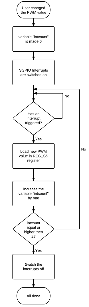
PWM example
An example is provided that uses SPGIO to create PWM signals, a flowchart of this example can be found on the next page.
Every SGPIO pin can be used as an extra PWM pin in this way.
The duty cycle and frequency can be changed on the fly.
As one slice has a 32-bit FIFO buffer there are only 33 PWM duty cycles possible,
so essentially it's a 5-bit PWM that can be fully on or fully off.
When concatenating slices a bigger precision can be reached but to make this example simple this is not implemented.
A slice is used as output and the PWM data is loaded in the REG and REG_SS data registers.
After that the slice only has to repeat the data in the REG register.
When the PWM duty cycle is changed the value in the REG_SS register will be updated twice.
This is because every 32 clock cycles the REG and REG_SS register is swapped.
If the data is only written in the REG_SS register once only half of the time the PWM output would be correct and half of the time it would be the old value.
When the command is executed to edit a PWM value the interrupts are switched on.
When the next swap between REG and REG_SS occurs the new data is loaded into the REG_SS register.
When another data swap occurs this happens again.
After this the interrupts are switched off and the PWM duty cycle is changed.
A flowchart of this can be found on the next page.
As the example uses internal clock (COUNT) and enables with OENREG and each PWM channel uses only one output slice,
OUT_MUX_CFG, SLICE_MUX_CFG are 0.
The data in the REG register has to be repeated so SGPIO_MUX_CFG bit 11 is set high.
This means the slice is in self loop mode and will repeat the data in the REG register.
The clock speed is dependent of what the user wants so it is calculated and then stored in the PRESET register.
As we exchange the REG and REG_SS registers every 32 bit, the POS_PRESET is 0x1F.
When the SGPIO slice is set up as a PWM pin the frequency can be specified by the user.
The code calculates the correct divider PRESET setting by the following formula.
PWM frequency * 32 = SGPIO_CLOCK / (PRESET +1)
Note the “* 32” in the above equation, this is because the PWM signal frequency is 32 times of the shift clock frequency.
How to use the SGPIO PWM library
The SGPIO PWM library has four commands:
- • void SGPIOPWMinit(void);
- • void SGPIOPWMchaninit(uint32_t freq, uint8_t channel);
- • void SGPIOPWMValue(uint8_t value, uint8_t channel);
- • uint8_t SGPIOPWMstatus();
SGPIOPWMinit initializes SGPIO for PWM use.
It disables all interrupts, makes all SGPIO slices an output and enables all SGPIO clocks.
This command should be executed before the other commands are used.
SGPIOPWMchaninit is the command to initialize an SGPIO slice for PWM use.
It can also be used to change the PWM frequency at any moment but can cause a small hiccup in the PWM signal.
“freq” is the desired PWM frequency in hertz.
The maximum frequency is the core clock divided by 64 (because the shift clock frequency is 32 times of the PWM frequency).
As it uses a divider the actual speed will be an approximate of the given frequency.
“channel” is the SGPIO slice that should be adjusted.
This command has to be executed before the SGPIOPWMValue works.
SGPIOPWMValue is used to change the PWM duty cycle of any slice.
As it is a 5-bit PWM that can be fully on or off there are 33 values.
0 is a 0% duty cycle, 33 is a 100% duty cycle and 16 is ~47% duty cycle.
Channel is the SGPIO slice that should be adjusted.
After adjusting the duty cycle of a slice the command SGPIOPWMstatus can be used to check if the adjusting is done so another slice can be adjusted.
If it returns 0 adjusting is done and the SGPIOPWMValue can be used again.
Before an IO pin can be used as SGPIO pin the correct setup has to be loaded in the pinmux.
The settings possible per IO pin can be found in chapter 14, LPC43xx Pin configuration in the user manual.
For example, to use P0_0 as SGPIO pin function 3 (SGPIO0) has to be selected.
The correct command for this is:
scu_pinmux(0x0, 0 , MD_PLN, FUNC3);
The example code uses P1.1, P2.6 and P2.8 to show some effects on a RGB LED.
To see this effect a common anode RGB LED should be connected to P1.1, P2.6 and P2.8.
The current HackRF design
entails using the SGPIO peripheral to move quadrature baseband receive and transmit data
between the USB interface and the baseband ADC/DAC IC.
Because the baseband ADC/DAC IC (MAX5864) uses DDR signaling, we expect to use a CPLD to convert bus signaling.
The CPLD may also help manage bus turnaround (between transmit and receive modes)
or interfacing two narrower but faster interfaces to the LPC43xx to facilitate full-duplex.
Because the Jellybean board wasn't completed at the time of these experiments,
I used the Diolan LPC-4350-DB1-A development board.
Despite using an LPC4350 in an BGA256 package, the SGPIO peripheral's signals can be mapped to many different pins.
So reworking code to a new set of SGPIO pins should be a trivial matter of switching the SGU configuration for the affected pins.
SGPIO Examples
Some SGPIO peripheral examples can be found in the LPCWare repository.
All source I've found so far is focused on generating many I2S interfaces,
which is not very similar to HackRF's needs.
But reviewing the code is still valuable in grasping how the SGPIO peripheral operates.
There are a few common details to setting up the SGPIO peripheral:
// Configure the PLL to generate a reasonable clock. The SGPIO
// will operate with a clock of up to 204MHz (the same as the
// M4 clock.
CGU_SetPLL1(12);

// Set the BASE_PERIPH clock to come from PLL1.
CGU_EnableEntity(CGU_BASE_PERIPH, ENABLE);
CGU_EntityConnect(CGU_CLKSRC_PLL1, CGU_BASE_PERIPH);

// Compute and commit clock configuration changes.
CGU_UpdateClock();
Jiggle SGPIO Pins From GPIO Mode
My first test was to ensure I had the right pin(s) hooked up to my scope:
// Jiggle one of the SGPIO pins in GPIO mode, to make sure
// I'm looking at the right pin on the scope.
scu_pinmux(9,  0, MD_PLN_FAST, 0);
GPIO_SetDir(4, 1L << 12, 1);
while(1) {
    volatile int i;
    GPIO_SetValue(4, 1L << 12);
    for(i=0; i<1000; i++);
    GPIO_ClearValue(4, 1L << 12);
    for(i=0; i<1000; i++);
}
Jiggle Pins from SGPIO Mode
You can also control SGPIO pins, GPIO-style, from within the SGPIO peripheral.
This helped me understand the basics of operating the SGPIO output mux.
// Set pin to SGPIO mode, toggle output using SGPIO
// peripheral registers.
scu_pinmux(9,  0, MD_PLN_FAST, 6);  // SGPIO0

// P_OUT_CFG = 4, gpio_out
// P_OE_CFG = X
LPC_SGPIO->OUT_MUX_CFG[0] = (0L << 4) | (4L << 0);
LPC_SGPIO->GPIO_OENREG |= (1L << 0);

while(1) {
    volatile int i;
    LPC_SGPIO->GPIO_OUTREG |= (1L << 0);
    for(i=0; i<1000; i++);
    LPC_SGPIO->GPIO_OUTREG &= ~(1L << 0);
    for(i=0; i<1000; i++);
}
Serializing Data With Slice Clock Source
My first full-on SGPIO experiment involved serializing a data pattern from slice A,
using slice D to generate a SGPIO_CLK/2 data rate.
I derived the code from examples that configured the SGPIO as I2S interfaces:
// Disable all counters during configuration
LPC_SGPIO->CTRL_ENABLED = 0;

// Configure pin functions.
scu_pinmux(9,  0, MD_PLN_FAST, 6);  // SGPIO0
scu_pinmux(2,  3, MD_PLN_FAST, 0);  // SGPIO12

// Enable SGPIO pin outputs.
LPC_SGPIO->GPIO_OENREG =
    (1L << 12) |    // SGPIO12
    (1L <<  0);     // SGPIO0

// SGPIO pin 0 outputs slice A bit 0.
LPC_SGPIO->OUT_MUX_CFG[0] =
    (0L <<  4) |    // P_OE_CFG = X
    (0L <<  0);     // P_OUT_CFG = 0, dout_doutm1 (1-bit mode)

// SGPIO pin 12 outputs slice D bit 0.
LPC_SGPIO->OUT_MUX_CFG[12] =
    (0L <<  4) |    // P_OE_CFG = X
    (0L <<  0);     // P_OUT_CFG = 0, dout_doutm1 (1-bit mode)

// Slice A
LPC_SGPIO->SGPIO_MUX_CFG[0] =
    (0L << 12) |    // CONCAT_ORDER = 0 (self-loop)
    (1L << 11) |    // CONCAT_ENABLE = 1 (concatenate data)
    (0L <<  9) |    // QUALIFIER_SLICE_MODE = X
    (0L <<  7) |    // QUALIFIER_PIN_MODE = X
    (0L <<  5) |    // QUALIFIER_MODE = 0 (enable)
    (0L <<  3) |    // CLK_SOURCE_SLICE_MODE = 0, slice D
    (0L <<  1) |    // CLK_SOURCE_PIN_MODE = X
    (0L <<  0);     // EXT_CLK_ENABLE = 0, internal clock signal (slice)

LPC_SGPIO->SLICE_MUX_CFG[0] =
    (0L <<  8) |    // INV_QUALIFIER = 0 (use normal qualifier)
    (0L <<  6) |    // PARALLEL_MODE = 0 (shift 1 bit per clock)
    (0L <<  4) |    // DATA_CAPTURE_MODE = 0 (detect rising edge)
    (0L <<  3) |    // INV_OUT_CLK = 0 (normal clock)
    (0L <<  2) |    // CLKGEN_MODE = 0 (use clock from COUNTER)
    (0L <<  1) |    // CLK_CAPTURE_MODE = 0 (use rising clock edge)
    (0L <<  0);     // MATCH_MODE = 0 (do not match data)

LPC_SGPIO->PRESET[0] = 1;
LPC_SGPIO->COUNT[0] = 0;
LPC_SGPIO->POS[0] = (0x1FL << 8) | (0x1FL << 0);
LPC_SGPIO->REG[0] = 0xAAAAAAAA;     // Primary output data register
LPC_SGPIO->REG_SS[0] = 0xAAAAAAAA;  // Shadow output data register

// Slice D (clock for Slice A)
LPC_SGPIO->SGPIO_MUX_CFG[3] =
    (0L << 12) |    // CONCAT_ORDER = 0 (self-loop)
    (1L << 11) |    // CONCAT_ENABLE = 1 (concatenate data)
    (0L <<  9) |    // QUALIFIER_SLICE_MODE = X
    (0L <<  7) |    // QUALIFIER_PIN_MODE = X
    (0L <<  5) |    // QUALIFIER_MODE = 0 (enable)
    (0L <<  3) |    // CLK_SOURCE_SLICE_MODE = 0, slice D
    (0L <<  1) |    // CLK_SOURCE_PIN_MODE = X
    (0L <<  0);     // EXT_CLK_ENABLE = 0, internal clock signal (slice)

LPC_SGPIO->SLICE_MUX_CFG[3] =
    (0L <<  8) |    // INV_QUALIFIER = 0 (use normal qualifier)
    (0L <<  6) |    // PARALLEL_MODE = 0 (shift 1 bit per clock)
    (0L <<  4) |    // DATA_CAPTURE_MODE = 0 (detect rising edge)
    (0L <<  3) |    // INV_OUT_CLK = 0 (normal clock)
    (0L <<  2) |    // CLKGEN_MODE = 0 (use clock from COUNTER)
    (0L <<  1) |    // CLK_CAPTURE_MODE = 0 (use rising clock edge)
    (0L <<  0);     // MATCH_MODE = 0 (do not match data)

LPC_SGPIO->PRESET[3] = 0;
LPC_SGPIO->COUNT[3] = 0;
LPC_SGPIO->POS[3] = (0x1FL << 8) | (0x1FL << 0);
LPC_SGPIO->REG[0] = 0xAAAAAAAA;     // Primary output data register
LPC_SGPIO->REG_SS[0] = 0xAAAAAAAA;  // Shadow output data register

// Start SGPIO operation by enabling slice clocks.
LPC_SGPIO->CTRL_ENABLED =
    (1L <<  3) |    // Slice D
    (1L <<  0);     // Slice A

